Junior FPGA Design Engineer: how to become?
Hello!
Sometimes novice developers are not very well aware of what literature should be read in order to seriously study a particular language.
Development under FPGA (FPGA) is not just any language. This is a very voluminous area, with a huge number of pitfalls and nuances.
')
In this article you will find:
Welcome under the cut!
It is necessary:
Literature :
Test questions :
This includes:
As an HDL language, I recommend first learning the most basic constructs of Verilog 'a, and then switching to SystemVerilog .
Literature :
Test questions :
Test items :
1. Draw a pattern from the base digital nodes for the following code:
2. Draw the behavior of the circuit from item 1 (i.e. the state of all “variables”) under the following input influences:
3. Write a module to control the traffic light, which will light red, yellow and green lights in the well-known sequence: red, red and yellow, green, green blinks, yellow, red. The parameters that specify the burning time of traffic lights and the flashing period of the green light are the parameters of the module. The time is set in the number of clock cycles clk_i .
Module Interface:
It is necessary:
Literature :
Video Tutorials :
Test questions :
It is necessary:
I work with Altera chips, so here and beyond the name of the families and utilities will be from this vendor. If you know similar literature for Xilinx - write in a personal or in the comments - I will definitely add it to the article.
Literature :
Video Tutorials :
Test questions :
In questions marked with (*) , of course, do not need to remember everything by heart, but you can use datasheets.
It is necessary:
Literature :
Test questions :
It is necessary:
Literature:
Video Tutorials :
Test questions :
I spent two semesters reading the FPGA Development course for senior students at universities in St. Petersburg. The course included both lectures and a set of laboratory works. Lectures were based on the literature listed above.
Course Plan:
Names of lectures (in 2015):
Lecture slides
Laboratory work :
In this part of the article I will talk about common mistakes that novice developers make, and give advice on how to fix them.
Symptoms :
Treatment :
Symptoms :
Treatment :
If you see oddities in SignalTap, then double-check whether the signals you are shooting with the “gating” frequency are synchronous.
Continuation of the first paragraph, but I decided to allocate it separately.
Symptoms are similar with the previous paragraph.
For some reason, many people like to do this:
Those. The input signal on the min_cnt trigger uses a different signal than the sync pulse clk_i . It is formed by combinational logic (the output of the comparator).
Or like this:
The input of the trigger sum comes the output of combinational logic, the input of which is powered by different clock signals.
Both examples are wrong , never do that! These examples are a clear violation of the rules of synchronous design.
I guess it all comes from the 2000s, when the chips were small and the developers survived as best they could.
Most likely at small frequencies (such as 1 MHz) it rolled, but if you are going to join a team that does serious things on top-end chips, then for such tricks you can easily fly out of the internship.
Treatment :
You make this mistake if the development looks like this:
Why is that bad:
Treatment :
If something does not work on iron, then:
Symptoms :
Treatment :
I hope that in this article I have revealed that it is necessary to read and know in order to enter the world of development for FPGA.
I am sure that if you:
you can easily claim the position of a junior in a serious company.
Of course, this path can not be mastered in one weekend. It may take a month and not one, but this path must be taken if you want to go from student FPGA to professional development.
Thanks for attention!
As always, I will be glad to questions and comments in the comments or in personal mail.
PS
Sometimes they write to me in PM:
Most often, I offer them to look at two references ( FPGA and JAVA ) and draw conclusions on their own.
Sometimes novice developers are not very well aware of what literature should be read in order to seriously study a particular language.
Development under FPGA (FPGA) is not just any language. This is a very voluminous area, with a huge number of pitfalls and nuances.
')
In this article you will find:
- the list of topics that a novice developer should master under FPGA
- recommended literature for each topic
- a set of test questions and laboratory work
- classic novice bugs (and correction tips)
Welcome under the cut!
What you need to know and be able to
Digital circuit design
It is necessary:
- know the basic digital nodes (logical elements AND / OR / NOT, encoders, multiplexers, totalizers, etc.)
Literature :
- David Harris, Sarah Harris. Digital Design and Computer Architecture is a very large book, telling from the Azov to the top. There is a version in Russian . I looked through the Russian version: it is read very quickly and easily.
- Ugryumov E.P. “Digital circuitry” is a classic
Soviettextbook, with all the ensuing consequences (some topics are explained too difficult, and you cannot immediately understand whether you need this information now or you can skip it). I read an older edition, perhaps in the 2010 edition, everything changed for the better, did not look.
Test questions :
- What is the difference between digital circuitry and analog?
- What are the basic digital nodes? In which of them the output depends only on the input?
- What is a multiplexer? Draw a 4 in 1 multiplexer circuit from the primitive elements AND / OR / NOT.
- Build a truth table for the expression: X = A or (B and C) or D.
HDL syntax
This includes:
- knowledge of synthesized constructs (syntax) HDL-language
- knowledge of how to describe basic digital nodes using an HDL language
- understanding of what (on the part of basic digital nodes) this or that piece of HDL code turns into
- ability to write in HDL language to get the desired behavior
As an HDL language, I recommend first learning the most basic constructs of Verilog 'a, and then switching to SystemVerilog .
Literature :
- Pong P. Chu. "FPGA prototyping by Verilog examples" - signs Verilog, starting with the basics. The syntax is detailed and there are a huge number of examples, both simple (counters) and higher levels (UART and VGA).
- Joseph Karshenboym. "Short course HDL" - a classic course in Russian.
- www.asic-world.com is a website with a bunch of examples on both Verilog and SystemVerilog.
- David Harris, Sarah Harris. Digital Design and Computer Architecture (see above)
- Stuart Sutherland. SystemVerilog for Design is a book about Verilog and SystemVerilog differences. Basic knowledge of Verilog is required to read. It is recommended to read to understand what amenities were introduced in the new standard.
Test questions :
- How is blocking assignment different from non-blocking? When should one apply when another?
- Is there a difference between the following three descriptions? If so, what is it manifested in?
// code 1: assign a = b + c; // code 2: always @( b or c ) begin a = b + c; end // code 3: always @( * ) begin a = b + c; end
Test items :
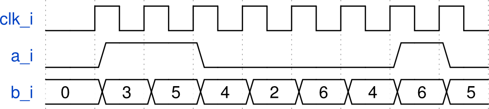
1. Draw a pattern from the base digital nodes for the following code:
Hidden text
module test( input clk_i, input a_i, input [2:0] b_i, output reg x_o ); reg [7:0] cnt = 8'd0; reg [7:0] cnt2; wire c; reg d; always @( posedge clk_i ) cnt <= cnt + 1'd1; always @(*) begin cnt2 = cnt + 1'd1; end assign c = ( cnt < 8'd5 ) && ( a_i == 1'b0 ); always @( posedge clk_i ) begin d <= c; x_o <= c ? ( d ) : ( cnt2[ b_i ] ); end endmodule 2. Draw the behavior of the circuit from item 1 (i.e. the state of all “variables”) under the following input influences:
Hidden text
Timeteps are drawn using the online WaveDrom editor.
3. Write a module to control the traffic light, which will light red, yellow and green lights in the well-known sequence: red, red and yellow, green, green blinks, yellow, red. The parameters that specify the burning time of traffic lights and the flashing period of the green light are the parameters of the module. The time is set in the number of clock cycles clk_i .
Module Interface:
Hidden text
module traffic_light( // c input clk_i, // input rst_i, // 1, , 0 — output red_o, output yellow_o, output green_o ); Simulation and verification of HDL-code
It is necessary:
- know the non-synthesized designs of Verilog and SystemVerilog
- be able to write a simple testbench, run it in the simulator (for example, ModelSim)
- understand how the “perfect” testbench should be arranged
Literature :
- testbench.in - a huge number of verification examples using Verilog'a and SystemVerilog'a.
- Chris Spear. “SystemVerilog for Verification” is a good, big book about verification using SystemVerilog. Reads easily, you can find answers to many questions.
Video Tutorials :
Test questions :
- How does function differ from task ?
- Imagine that you wrote the simplest HDL model of a 5-stage RISC processor. How will you verify it? (The issue of increased complexity ).
- What is the difference between a queue and a mailbox (data types in the SystemVerilog language)?
- What is the difference between functional simulation and temporary one? When what should be used?
Fpga
It is necessary:
- know what basic elements the FPGA consists of
- Understand how workflow development happens under FPGA
- Intuitively imagine which operations for FPGA are cheap and which are expensive (in terms of frequency and resources)
I work with Altera chips, so here and beyond the name of the families and utilities will be from this vendor. If you know similar literature for Xilinx - write in a personal or in the comments - I will definitely add it to the article.
Literature :
- Andrew Moore. “FPGAs for Dummies” is a story about FPGA in a very high-level (marketing) language. You can look with one eye.
- Altera Cyclone III Handbook - datasheet on the relatively old FPGA family from Altera.
- Steve Kilts. "Advanced FPGA Design" - a class book, reveals many nuances of development.
Video Tutorials :
- Altera. Basics of Programmable Logic: FPGA Architecture
- David L. Jones (EEVblog). “What Is An FPGA?” Is a smart video with a story about what FPGA is.
Test questions :
- What is the difference between FPGA and ASIC? What blocks does the FPGA consist of (or can it consist of)?
- Try to outline the range of tasks for which it is good (economically feasible) to use FPGA, and for which MCU and CPU?
- What hardware blocks do you know? What are they used for? (By hardware blocks we mean Hard IP ).
- The Y family uses LUT with three inputs and one output. What is the minimum number of LUTs to calculate assign eq = (a == b); if a and b are 32-bit positive integers? And if LUT has four (five, six) inputs?
- You need to create a single-port memory of 16 words. Each word is 100 bits wide. How many M9K blocks (9216 bits) will be occupied? We believe that we are doing a project under Cyclone III. (*)
In questions marked with (*) , of course, do not need to remember everything by heart, but you can use datasheets.
Synchronous design and everything related to timings
It is necessary:
- know the principle of synchronous design
- know the negative consequences of one or another scheme
- to have the concept of constrains
Literature :
- Steve Kilts. “Advanced FPGA Design” (see above).
- Altera. The Quartus Handbook is the Recommended Design Practices chapter.
- Altera. Understanding Metastability
- nerudo. "Metastability trigger and inter-cycle synchronization"
Test questions :
- What are timing constraints? Where are they described and what are they for (what are they used for)? What happens if you do not describe them?
- What is clock domain crossing ? How and when should it be carried out?
- What is the difference between synchronous and asynchronous reset? What will happen if a synchronous reset input has an asynchronous reset?
- What is a latch (latch, latch)? What are the consequences of using latch? Give an example of the code that creates latch.
- What is a combination loop? What are the consequences of using a combination loop?
- What is metastability ? How to achieve it? What are its pros and cons?
- What is a glitch? Do I need to deal with this? And if so, where and how?
- What is setup time / hold time for a D-trigger?
CAD
It is necessary:
- be able to create a project
- be able to describe I / O pins and constrains (at least for simple situations, without complex I / O interfaces)
- know what build reports there are, what information is contained in each of them
- be able to use the debugging tool on the hardware
- be able to use the tool for the analysis of timings ( STA )
- know what ready IP cores / modules (FIFO, RAM, FFT, DDR, Ethernet, etc.) the vendor provides and how you can add them to the project
Literature:
- Altera. "Quartus Handbook"
- Altera. SignalTap II with Verilog Designs
- Denis Shehelev. “Synopsys Design Constraint - language for setting time constraints on the example of Altera TimeQuest” is a good series of articles in Russian. see also TimeQuest for Dummies .
Video Tutorials :
- Altera. The Quartus Prime Software: Foundation.
- Altera. “Using the Quartus Prime Software: An Introduction”.
- Altera. "The Quartus II Software Interactive Tutorial".
- Altera. "TimeQuest Timing Analyzer"
Test questions :
- What stages of assembly occur from clicking on the “Collect the project completely” button to get the finished binary file? What happens at each stage?
- How to see if the CAD was able to put the project in the specified constraints (constraints)?
Lectures and laboratory
I spent two semesters reading the FPGA Development course for senior students at universities in St. Petersburg. The course included both lectures and a set of laboratory works. Lectures were based on the literature listed above.
Course Plan:
Hidden text
: * ? . * ( Quartus ). Verilog: * ( HDL ). * / . * : * . * , / * . * . * . * / . * . * Verilog . * ( +SystemVerilog ): * . . Testbench. testbench. * testbench'. * . . * ( , .. ). * tasks. * . * . * SystemVerilog Assertions. * testbench . * c ( ) . Names of lectures (in 2015):
- Introduction to FPGA.
- Internal FPGA device.
- Introduction to Verilog / SystemVerilog. Examples of the description of various types of logic.
- Synchronous design. Create simple testbenches.
- Description of FSM, arrays and structures in SystemVerilog. Memory: creation with Verilog and MegaWizard.
- How DCFIFO works. Static Timing Analysis. TimeQuest, constraints.
- Verification: coverage, assertions, SystemVerilog interfaces
- Interfaces family Avalon. IP Cores. Qsys.
- Verification: SystemVerilog OOP, constrained-random tests.
Lecture slides
Hidden text
Unfortunately, these are the SLIDES who helped me to give lectures (not all the course information is contained on the slides, some I used as a support, and the material was given on the board).
Sometimes there will be pictures that are not related to the neighboring ones (for example, tasks for tests that were given at lectures).
Sometimes there will be pictures that are not related to the neighboring ones (for example, tasks for tests that were given at lectures).
Laboratory work :
Classic mistakes
In this part of the article I will talk about common mistakes that novice developers make, and give advice on how to fix them.
Confusion in assignments (blocking and non-blocking)
Symptoms :
- you are not very confident about the question of blocking and non-blocking assignments (see above)
- you notice that you randomly change "=" to "<=" (and vice versa), hoping that it will work
- the simulator shows weird things, you start to doubt that you understand how the D-trigger works
- simulation results do not consistently coincide with what is happening on the gland (somewhere, something is floating in tact)
Treatment :
- Understand the Verilog material (see literature above)
- if you want the simulation result to coincide with what will be synthesized and embodied on the hardware, remember a simple rule: in blocks that describe combinational logic ( always_comb , always @ (*) ), you must use only blocking assignments ( = ). In the blocks that describe the triggers ( always_ff , always @ (posedge clk ...) ) you are obliged to use only non-blocking assignments ( <= ).
Timing problem
Symptoms :
- simulation results do not match what is happening on the gland
- iron is unstable: sometimes clearly visible interference (for example, on VGA)
- "I added a signal tap, and after that the circuit stopped working correctly, I removed the signal tap and everything is fine"
Treatment :
- register all the necessary constraints (at least the used clock frequency (or frequencies) in the * .sdc file), connect this file to the project
- recompile the project. Go to TimeQuest and see if there are negative weak ones, and if there is, then further understand why this happens (perhaps it’s enough to twist the settings in Quartus, or you have to rewrite the pieces of code).
If you see oddities in SignalTap, then double-check whether the signals you are shooting with the “gating” frequency are synchronous.
Not following the principles of synchronous design (asynchronous)
Continuation of the first paragraph, but I decided to allocate it separately.
Symptoms are similar with the previous paragraph.
For some reason, many people like to do this:
// BAD EXAMPLE ... input clk_i, ... logic [7:0] sec_cnt; logic [7:0] min_cnt; logic last_sec_value; assign last_sec_value = ( sec_cnt == 8'd59 ); always_ff @( posedge clk_i ) if( last_sec_value ) sec_cnt <= 'd0; else sec_cnt <= sec_cnt + 1'd1; always_ff @( posedge last_sec_value ) min_cnt <= min_cnt + 1'd1; Those. The input signal on the min_cnt trigger uses a different signal than the sync pulse clk_i . It is formed by combinational logic (the output of the comparator).
Or like this:
// BAD EXAMPLE ... input clk_a_i, input clk_b_i, ... logic [7:0] cnt_a; logic [7:0] cnt_b; logic [7:0] sum; always_ff @( posedge clk_a_i ) cnt_a <= cnt_a + 1'd1; always_ff @( posedge clk_b_i ) cnt_b <= cnt_b + 1'd1; always_ff @( posedge clk_b_i ) sum <= cnt_a + cnt_b; The input of the trigger sum comes the output of combinational logic, the input of which is powered by different clock signals.
Both examples are wrong , never do that! These examples are a clear violation of the rules of synchronous design.
I guess it all comes from the 2000s, when the chips were small and the developers survived as best they could.
Most likely at small frequencies (such as 1 MHz) it rolled, but if you are going to join a team that does serious things on top-end chips, then for such tricks you can easily fly out of the internship.
Treatment :
- go through the whole project, write out (on a piece of paper) what clocking clock (signal) is used for each trigger.
- understand how this number can be reduced to the minimum number (within reasonable limits, of course), correct the code according to the rules of synchronous design.
- go through the whole project and carefully track how clock domain crossing happens (i.e. data transfer from one frequency to another). Correct if it happens incorrectly.
- perform all steps from the “Problem in Timings” .
Continuous debugging on hardware (ignoring simulation)
You make this mistake if the development looks like this:
- edit hdl file
- complete project compilation
- flashing binary on board
- connection using SignalTap, viewing the desired signals
- understanding of the error, the transition to claim 1
Why is that bad:
- with SignalTap, you cannot see all the signals if you have a large project
- you take your time, or the time of your employer, when compiling a complete project, because this may take considerable time. On small chips, it takes 5-10 minutes, and you can type and score and go at this time to smoke / drink tea / play kicker, but on large projects this will go sideways.
- need a working board at hand
- you are not sure that the changes in the code are working and will not break something else
Treatment :
- write a testbench for the entire project, or for its parts
- achieve proper operation in the simulation
- build a project, check on the board
If something does not work on iron, then:
- walk on the points indicated above (timings and asynchronous)
- if there are no problems in timings, then try to understand at what input influences this happens
- submit these effects in the simulation, make sure that the problem is reproduced
- correct the error in the RTL code, check in the simulation and on the hardware
- Required : conclude why the previous version of the simulation could not catch this error
No development rules (+ code with backfill )
Symptoms :
- You spend a lot of time reading (parsing) the code you wrote yesterday.
- You often write the same type of code (the most popular keys on your keyboard are Ctrl + C and Ctrl + V )
- you cannot understand the code that your colleague wrote (if you are working together on one module / IP core), and it is yours.
Treatment :
- Get acquainted with the literature that tells how to write good code, for example, McConnell. "Perfect Code"
- develop and describe the development rules for the team. Or use ready-made: NetFPGA , discussion on electronix # 1 , discussion on electronix # 2 , or one that I use.
- Give your review code to more experienced developers. You can ask about this on the electronix forum in the appropriate section. Of course, it is desirable that something more serious than the blinking of the LEDs, otherwise you just will not understand :).
Conclusion
I hope that in this article I have revealed that it is necessary to read and know in order to enter the world of development for FPGA.
I am sure that if you:
- can easily answer the test questions above (without memorization, of course)
- decide correctly laboratory work
- get rid of the "classic mistakes"
- execute 1-2 projects on githab and check them on hardware. (preferably more complicated than blinking LEDs and watches).
you can easily claim the position of a junior in a serious company.
Of course, this path can not be mastered in one weekend. It may take a month and not one, but this path must be taken if you want to go from student FPGA to professional development.
Thanks for attention!
As always, I will be glad to questions and comments in the comments or in personal mail.
PS
Sometimes they write to me in PM:
Good day.
I am a student of 3 (4, 5) courses of such a university.
I like the idea of writing under FPGA (concurrency, you can do what you want, blah blah blah) and like Java (made simple Android applications). I want to do something of this more or less seriously. What do you advise to teach?
Most often, I offer them to look at two references ( FPGA and JAVA ) and draw conclusions on their own.
Source: https://habr.com/ru/post/281525/
All Articles