STM32 and LCD, fast screen fill
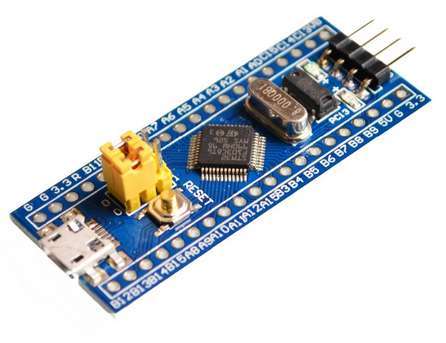
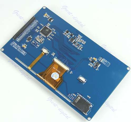
At present, various liquid crystal displays, which are perfectly connected to the STM32 family of controllers, have become popular. This article will discuss one of the common STM32F103C8T6 controllers and a 7 "display on the SSD1963 controller. Both as finished units are easily available on Aliexpress and are relatively inexpensive. Of course, everything discussed below is true for other displays with a parallel interface and most STM32 controllers .
Here are the connectable devices:
')
Included with the display was pinout pinouts and initialization code for the 51st controller with comments in the language of the manufacturer.
Connecting the display consists in supplying 3.3 and 5 volts of power to the required outputs and connecting the information lines to the controller. Control signals D / C, WE, RST are connected to free I / O lines on the processor. In our case, this is D / C - PA1, WE - PA8, RST - PA2. The signals RD and CS can be not used, and a logical unit must be supplied to the RD, i.e. connect via a resistor (in this case, 4.7 kOhm) to +3.3 V, and to CS - “0”, i.e. connect to the ground.
Next you need to connect the data bus. In this display, it is assumed to be 16-bit, but it is possible to select 8 and 9 bit modes of operation during initialization. That is, you need to connect at least the display lines DB0-DB7, as well as the maximum DB8-DB15. For ease of programming and minimizing data conversion commands, it is better to add them to one I / O group. If we consider the option of a 16-bit data bus, then it is not necessary to choose on this microcontroller - only PB0 - PB15.
We connect them accordingly with the DB0-DB15 display:
There are a lot of unconnected contacts on the display comb, do not be confused by this. It has an SD memory card slot, a screen sensor, there is even an EEPROM memory card layout, but it is missing. These devices and occupy the rest of the connector. By the way, a 40-pin display connector is ideal for the PATA cable of computer hard drives.
The original code was transferred almost unchanged to the project, only conditional compilation was added to select the data bus width (initialization and commands go over an 8-bit bus, regardless of this mode).
In the code, there is no initialization of I / O ports and a system timer, based on which millisecond delays are realized (delay_ms ()).
After performing initialization:
We see the garbage of video memory on the display:
Now I want to erase this garbage and fill the screen with some color. In the source from the manufacturer the necessary material for writing the code is present. We use it.
As you can see, the code depends on the selected bus width. Accordingly, the time required for the transfer of the pixel to the display depends. For a 16-bit bus, a pixel is transmitted in one transmission cycle over the data bus, for a 9-bit bus — for two, for an 8-bit bus — for 3. Where does this data come from? From the documentation on SSD1963.

In the table you can find the location of each color component of the pixel, depending on the mode. The project uses 8-bit, 9-bit and 16-bit modes (565 format). As you can see, it was also possible to use the “clean” 16-bit format for more accurate color coding, but it also requires three cycles of data transmission over the bus. We cannot use the 18 and 24 bit formats because there is only a 16-bit bus at the display output.
So, with what speed we can fill the display on a processor with a clock frequency of 72 MHz?
176 ms - 16-bit bus
374 ms - 9-bit bus
470 ms - 8-bit bus
Not very fast, of course, but it may be enough to display slowly changing information. Of course, a 16-bit bus looks more attractive, and perhaps it will suit someone, but it takes too many I / O ports, which may then not be enough to connect other devices to the processor.
Let's try to consider a compromise version - 9 bits, as winning almost 0.1 s for the 8-bit version at the expense of just one additional I / O port.
Let's try to speed up the process of pouring the display. What if you reduce the number of logical operations within a loop?
Changed the color coding instead of the 16-bit variable in the RGB565 format, we use 32-bit, using only 18 of them in the RGB666 format. In addition, we introduced a temporary variable to store the value of the register LCD_DATA_PORT-> ODR during two cycles of outputting 9-bit data to the bus. Here it is necessary to make a reservation that it is not always possible, because during the output, the status of other ports of the GPIO B group configured for output can be changed at this time in the interrupt and the program will not work correctly. However, in our case there are no such problems and we check what we have achieved. So after the first optimization, the screen is filled in 9-bit mode for 298 ms. If you do not use the variable and work with the current state of the port, then there is also a speed increase, although not so significant - 335 ms:
For the sake of speed, it is also possible to sacrifice the possibility of using the remaining ports of group B in the output mode and to remove the logical operations related to maintaining their state:
It is clear that in the input mode and in alternative functions the possibility of use will be preserved, they are not dependent on the register ODR.
This will give some more acceleration, up to 246 ms.
Moving on.
The next step is to move the main loop through the pixels in the function to a deeper level and try to make a software version of the DMA channel emulation, direct memory access. To do this, we need to transfer the display control line WE to the group where the data bus is located, i.e. GPIO B. Let it be PB9.
As can be seen from the code, we sequentially write 4 data options to the port B group, where, in addition to the 9-bit data bus, the WE signal is also located. The operation "| 0x0200" is just setting this signal. This code gives a great boost up to 85 ms, and if you replace the definition of the array “static uint32_t dp [4]” by “static uint16_t dp [4]”, then up to 75 ms. For verification, a variant with the inclusion of the DMA mode and the same transfer of the contents of 4 cells to the I / O port was measured. The result is only 230 ms. Why is DMA slower? Everything is simple, in the program mode the compiler optimizes the code and all 4 values are placed in the registers of the processor, and not in memory, and the selection from memory that is performed by the DMA controller is much slower than working with registers.
The compiled main loop looks like this:
In this variant, as well as in the variant with the DMA channel, the restriction on the use of ports PB10-PB15 remains. However, they can display the signals of the display RST and D / C and take them into account in the cycle, then the restrictions will be less.
Thus, we have reached the maximum speed of filling the entire screen or a rectangular area with one color. It seems to be the limit, but you can enter another restriction and move a little further.
The fact is that in some applications, the display does not need the entire set of colors (in RGB656 - 65536 colors). For example, in the field of automated process control systems, where you want to display the state of the production facility, or some textual application, display of messages. If this assumption is correct, and we do not need to display full-color photos and video materials, then we will try to continue the optimization.
Consider a palette, where each color is equal to the first and second part of the data transmitted via the bus in the display. Those. Of the 18 bits of the RGB666 model, the first 9 bits are equal to the second 9. This gives us 2 ^ 9 = 512 colors. It may not seem enough to anyone, but it may well be enough to build graphs or display alphanumeric information. Let's call them conditionally "symmetrical colors."
What gives us the use of only these colors? Yes, the fact that to fill the area we do not need to change the state of the data bus in the process of filling. It is enough to switch the state of the signal WE and count how many times we have done it. Moreover, we can invert the WE for as long as necessary, the main thing is not less than what is needed to fill the area. It is easy to calculate that once per pixel we need to transfer two data blocks on the bus, then 2 acknowledgments with the signal WE are required. Accordingly, the full screen is necessary (screen_ width * screen_ length * 2) pulses, or 800 * 480 * 2 = 768000.
How easy it is to generate pulses. Of course! You can use a timer. TIM1 in this controller is faster than TIM2-TIM4 timers, because located on the faster APB2 clocking bus. Studies have shown that by turning on the timer in the PWM generator mode with a minimum divider, you can get a fill time of 32 ms! It is clear that the WE signal should be removed from the timer output, for example PA8 (TIM1_CH1).
Can I still increase the fill rate? It turned out yes, just by sending a SYSCLK signal from the RCC_MCO output to the WE LCD input. This is the maximum available frequency on the processor, 72 MHz. The time to fill the display with a symmetrical color is 10.7 ms.
The time is counted by the timer, after which the signal is removed by interruption, and the port switches to the output mode.
The timer counts the time with an accuracy of 1/72 µs for the number of points less than 32000 and with an accuracy of 1 µs for more points. This is due to the bit counter timer. Given that it takes some time to process the interrupt when the timer is turned off, the signal at the MCO output is removed a little later than required, with a small margin. It was established experimentally that it is about 10-11 clock speeds of the processor. Thus, we can say that there is a threshold for using this technique, at which it remains faster, despite the overhead of initializing the timer and RCC_MCO and shutting down. A square of 2x2 pixels is probably more profitable to programmatically fill the cycle.
As an output, it can be said that by adding some restrictions, the screen filling time was reduced from 375 to 11 ms. In addition, the filling is without the participation of the processor, which at this time can perform other tasks.
I will be glad comments and additions.
Here are the connectable devices:
')
Included with the display was pinout pinouts and initialization code for the 51st controller with comments in the language of the manufacturer.
Briefly about connecting
Connecting the display consists in supplying 3.3 and 5 volts of power to the required outputs and connecting the information lines to the controller. Control signals D / C, WE, RST are connected to free I / O lines on the processor. In our case, this is D / C - PA1, WE - PA8, RST - PA2. The signals RD and CS can be not used, and a logical unit must be supplied to the RD, i.e. connect via a resistor (in this case, 4.7 kOhm) to +3.3 V, and to CS - “0”, i.e. connect to the ground.
Comment
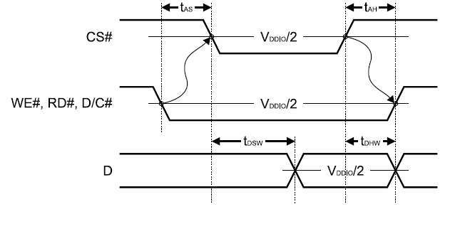
The display is configured by the manufacturer for operation of the interface in the 8080 mode, and, according to the documentation, the CS “chip select” signal must be enabled:
Initially, he worked. However, as the verification showed, if you do not want to use the data bus for other purposes, it is not needed.
Initially, he worked. However, as the verification showed, if you do not want to use the data bus for other purposes, it is not needed.
Next you need to connect the data bus. In this display, it is assumed to be 16-bit, but it is possible to select 8 and 9 bit modes of operation during initialization. That is, you need to connect at least the display lines DB0-DB7, as well as the maximum DB8-DB15. For ease of programming and minimizing data conversion commands, it is better to add them to one I / O group. If we consider the option of a 16-bit data bus, then it is not necessary to choose on this microcontroller - only PB0 - PB15.
We connect them accordingly with the DB0-DB15 display:
Comment
Of course there is also PA0-PA15, but if we want to use ST-Link for debugging, then a couple of them are already taken.
There are a lot of unconnected contacts on the display comb, do not be confused by this. It has an SD memory card slot, a screen sensor, there is even an EEPROM memory card layout, but it is missing. These devices and occupy the rest of the connector. By the way, a 40-pin display connector is ideal for the PATA cable of computer hard drives.
Like this
Display initialization
The original code was transferred almost unchanged to the project, only conditional compilation was added to select the data bus width (initialization and commands go over an 8-bit bus, regardless of this mode).
Code
#define SET_LCD_RDS LCD_RDS_PORT->BSRR = LCD_RDS #define RESET_LCD_RDS LCD_RDS_PORT->BRR = LCD_RDS #define SET_LCD_WR LCD_WR_PORT->BSRR = LCD_WR #define RESET_LCD_WR LCD_WR_PORT->BRR = LCD_WR #define SET_LCD_RST LCD_RST_PORT->BSRR = LCD_RST #define RESET_LCD_RST LCD_RST_PORT->BRR = LCD_RST void SSD1963_Init (void) { uint16_t HDP=799; uint16_t HT=928; uint16_t HPS=46; uint16_t LPS=15; uint8_t HPW=48; uint16_t VDP=479; uint16_t VT=525; uint16_t VPS=16; uint16_t FPS=8; uint8_t VPW=16; RESET_LCD_RST; delay_ms(5); SET_LCD_RST; delay_ms(5); SSD1963_WriteCommand(0x00E2); //PLL multiplier, set PLL clock to 120M SSD1963_WriteData(0x0023); //N=0x36 for 6.5M, 0x23 for 10M crystal SSD1963_WriteData(0x0002); SSD1963_WriteData(0x0004); SSD1963_WriteCommand(0x00E0); // PLL enable SSD1963_WriteData(0x0001); delay_ms(1); SSD1963_WriteCommand(0x00E0); SSD1963_WriteData(0x0003); delay_ms(5); SSD1963_WriteCommand(0x0001); // software reset delay_ms(5); SSD1963_WriteCommand(0x00E6); //PLL setting for PCLK, depends on resolution SSD1963_WriteData(0x0003); SSD1963_WriteData(0x00ff); SSD1963_WriteData(0x00ff); SSD1963_WriteCommand(0x00B0); //LCD SPECIFICATION SSD1963_WriteData(0x0000); SSD1963_WriteData(0x0000); SSD1963_WriteData((HDP>>8)&0X00FF); //Set HDP SSD1963_WriteData(HDP&0X00FF); SSD1963_WriteData((VDP>>8)&0X00FF); //Set VDP SSD1963_WriteData(VDP&0X00FF); SSD1963_WriteData(0x0000); SSD1963_WriteCommand(0x00B4); //HSYNC SSD1963_WriteData((HT>>8)&0X00FF); //Set HT SSD1963_WriteData(HT&0X00FF); SSD1963_WriteData((HPS>>8)&0X00FF); //Set HPS SSD1963_WriteData(HPS&0X00FF); SSD1963_WriteData(HPW); //Set HPW SSD1963_WriteData((LPS>>8)&0X00FF); //Set HPS SSD1963_WriteData(LPS&0X00FF); SSD1963_WriteData(0x0000); SSD1963_WriteCommand(0x00B6); //VSYNC SSD1963_WriteData((VT>>8)&0X00FF); //Set VT SSD1963_WriteData(VT&0X00FF); SSD1963_WriteData((VPS>>8)&0X00FF); //Set VPS SSD1963_WriteData(VPS&0X00FF); SSD1963_WriteData(VPW); //Set VPW SSD1963_WriteData((FPS>>8)&0X00FF); //Set FPS SSD1963_WriteData(FPS&0X00FF); SSD1963_WriteCommand(0x00BA); SSD1963_WriteData(0x0005); //GPIO[3:0] out 1 SSD1963_WriteCommand(0x00B8); SSD1963_WriteData(0x0007); //GPIO3=input, GPIO[2:0]=output SSD1963_WriteData(0x0001); //GPIO0 normal SSD1963_WriteCommand(0x0036); //rotation SSD1963_WriteData(0x0000); SSD1963_WriteCommand(0x00F0); //pixel data interface #if DATAPIXELWIDTH==16 SSD1963_WriteData(0x0003); //16 bit (565) #endif #if DATAPIXELWIDTH==9 SSD1963_WriteData(0x0006); // 9 bit #endif #if DATAPIXELWIDTH==8 SSD1963_WriteData(0x0000); // 8 bit #endif delay_ms(5); SSD1963_WriteCommand(0x0029); //display on SSD1963_WriteCommand(0x00d0); SSD1963_WriteData(0x000d); } void SSD1963_WriteCommand(uint16_t commandToWrite) { LCD_DATA_PORT->ODR = commandToWrite; RESET_LCD_RDS; RESET_LCD_WR; SET_LCD_WR; } void SSD1963_WriteData(uint16_t dataToWrite) { LCD_DATA_PORT->ODR = dataToWrite; SET_LCD_RDS; RESET_LCD_WR; SET_LCD_WR; } In the code, there is no initialization of I / O ports and a system timer, based on which millisecond delays are realized (delay_ms ()).
After performing initialization:
tick_init(); // lcd_port_init(); // - SSD1963_Init(); // We see the garbage of video memory on the display:
Garbage
Display fill
Now I want to erase this garbage and fill the screen with some color. In the source from the manufacturer the necessary material for writing the code is present. We use it.
Code
// Fills whole screen specified color void SSD1963_SetArea(uint16_t x1, uint16_t x2, uint16_t y1, uint16_t y2) { SSD1963_WriteCommand(0x002a); SSD1963_WriteData((x1 >> 8) & 0xff); SSD1963_WriteData(x1 & 0xff); SSD1963_WriteData((x2 >> 8) & 0xff); SSD1963_WriteData(x2 & 0xff); SSD1963_WriteCommand(0x002a); SSD1963_WriteData((y1 >> 8) & 0xff); SSD1963_WriteData(y1 & 0xff); SSD1963_WriteData((y2 >> 8) & 0xff); SSD1963_WriteData(y2 & 0xff); } #if DATAPIXELWIDTH==16 void SSD1963_WriteDataPix(uint16_t pixdata) { LCD_DATA_PORT->ODR = pixdata; SET_LCD_RDS; RESET_LCD_WR; SET_LCD_WR; } #endif #if DATAPIXELWIDTH==9 void SSD1963_WriteDataPix(uint16_t pixdata) { LCD_DATA_PORT->ODR = (LCD_DATA_PORT->ODR & 0xfe00) | ((pixdata >> 8) & 0x000f) | ((pixdata >> 7) & 0x01f0); SET_LCD_RDS; RESET_LCD_WR; SET_LCD_WR; LCD_DATA_PORT->ODR = (LCD_DATA_PORT->ODR & 0xfe00) | ((pixdata << 1) & 0x01f7) | (pixdata & 0x0001); RESET_LCD_WR; SET_LCD_WR; } #endif #if DATAPIXELWIDTH==8 void SSD1963_WriteDataPix(uint16_t pixdata) { LCD_DATA_PORT->ODR = (LCD_DATA_PORT->ODR & 0xff00) | ((pixdata >> 8) & 0x00f8) | ((pixdata >> 9) & 0x0004); SET_LCD_RDS; RESET_LCD_WR; SET_LCD_WR; LCD_DATA_PORT->ODR = (LCD_DATA_PORT->ODR & 0xff00) | ((pixdata >> 3) & 0x00fc); RESET_LCD_WR; SET_LCD_WR; LCD_DATA_PORT->ODR = (LCD_DATA_PORT->ODR & 0xff00) | ((pixdata << 3) & 0x00f8) | ((pixdata << 2) & 0x0004); RESET_LCD_WR; SET_LCD_WR; } #endif void SSD1963_ClearScreen(uint16_t color) { unsigned int x,y; SSD1963_SetArea(0, TFT_WIDTH-1 , 0, TFT_HEIGHT-1); SSD1963_WriteCommand(0x002c); for(x=0;x<TFT_WIDTH;x++){ for(y= 0;y<TFT_HEIGHT;y++){ SSD1963_WriteDataPix(color); } } } As you can see, the code depends on the selected bus width. Accordingly, the time required for the transfer of the pixel to the display depends. For a 16-bit bus, a pixel is transmitted in one transmission cycle over the data bus, for a 9-bit bus — for two, for an 8-bit bus — for 3. Where does this data come from? From the documentation on SSD1963.
In the table you can find the location of each color component of the pixel, depending on the mode. The project uses 8-bit, 9-bit and 16-bit modes (565 format). As you can see, it was also possible to use the “clean” 16-bit format for more accurate color coding, but it also requires three cycles of data transmission over the bus. We cannot use the 18 and 24 bit formats because there is only a 16-bit bus at the display output.
So, with what speed we can fill the display on a processor with a clock frequency of 72 MHz?
176 ms - 16-bit bus
374 ms - 9-bit bus
470 ms - 8-bit bus
Not very fast, of course, but it may be enough to display slowly changing information. Of course, a 16-bit bus looks more attractive, and perhaps it will suit someone, but it takes too many I / O ports, which may then not be enough to connect other devices to the processor.
Let's try to consider a compromise version - 9 bits, as winning almost 0.1 s for the 8-bit version at the expense of just one additional I / O port.
Waveform
Speed optimization
Let's try to speed up the process of pouring the display. What if you reduce the number of logical operations within a loop?
// 18- RGB666 void SSD1963_WriteDataPix_9(uint32_t pixdata) { uint32_t tmp = (LCD_DATA_PORT->ODR & 0xfe00); SET_LCD_RDS; LCD_DATA_PORT->ODR = tmp | ((pixdata >> 9) & 0x01ff); RESET_LCD_WR; SET_LCD_WR; LCD_DATA_PORT->ODR = tmp | (pixdata & 0x01ff); RESET_LCD_WR; SET_LCD_WR; } // 18- RGB666 void SSD1963_ClearScreen_9(uint32_t color) { unsigned int x,y; SSD1963_SetArea(0, TFT_WIDTH-1 , 0, TFT_HEIGHT-1); SSD1963_WriteCommand(0x002c); for(x=0;x<TFT_WIDTH;x++) { for(y= 0;y<TFT_HEIGHT;y++) { SSD1963_WriteDataPix_9(color); } } } Changed the color coding instead of the 16-bit variable in the RGB565 format, we use 32-bit, using only 18 of them in the RGB666 format. In addition, we introduced a temporary variable to store the value of the register LCD_DATA_PORT-> ODR during two cycles of outputting 9-bit data to the bus. Here it is necessary to make a reservation that it is not always possible, because during the output, the status of other ports of the GPIO B group configured for output can be changed at this time in the interrupt and the program will not work correctly. However, in our case there are no such problems and we check what we have achieved. So after the first optimization, the screen is filled in 9-bit mode for 298 ms. If you do not use the variable and work with the current state of the port, then there is also a speed increase, although not so significant - 335 ms:
void SSD1963_WriteDataPix_9(uint32_t pixdata) { SET_LCD_RDS; LCD_DATA_PORT->ODR = (LCD_DATA_PORT->ODR & 0xfe00) | ((pixdata >> 9) & 0x01ff); RESET_LCD_WR; SET_LCD_WR; LCD_DATA_PORT->ODR = (LCD_DATA_PORT->ODR & 0xfe00) | (pixdata & 0x01ff); RESET_LCD_WR; SET_LCD_WR; } For the sake of speed, it is also possible to sacrifice the possibility of using the remaining ports of group B in the output mode and to remove the logical operations related to maintaining their state:
void SSD1963_WriteDataPix_9(uint32_t pixdata) { SET_LCD_RDS; LCD_DATA_PORT->ODR = pixdata >> 9; RESET_LCD_WR; SET_LCD_WR; LCD_DATA_PORT->ODR = pixdata; RESET_LCD_WR; SET_LCD_WR; } It is clear that in the input mode and in alternative functions the possibility of use will be preserved, they are not dependent on the register ODR.
This will give some more acceleration, up to 246 ms.
Waveform
Moving on.
The next step is to move the main loop through the pixels in the function to a deeper level and try to make a software version of the DMA channel emulation, direct memory access. To do this, we need to transfer the display control line WE to the group where the data bus is located, i.e. GPIO B. Let it be PB9.
void SSD1963_WriteDataPix_9(uint32_t pixdata, uint32_t n){ static uint32_t dp[4]; uint8_t i; SET_LCD_RDS; RESET_LCD_WR; dp[0] = (pixdata >> 9) & 0x01ff; dp[1] = ((pixdata >> 9) & 0x01ff) | 0x0200; dp[2] = pixdata & 0x01ff; dp[3] = (pixdata & 0x01ff) | 0x0200; for (;n;n--){ for (i=0;i<4;i++) { LCD_DATA_PORT->ODR = dp[i]; } } void SSD1963_ClearScreen_9(uint32_t color) { SSD1963_SetArea(0, TFT_WIDTH-1 , 0, TFT_HEIGHT-1); SSD1963_WriteCommand(0x002c); SSD1963_WriteDataPix_9(color, TFT_HEIGHT*TFT_WIDTH); } As can be seen from the code, we sequentially write 4 data options to the port B group, where, in addition to the 9-bit data bus, the WE signal is also located. The operation "| 0x0200" is just setting this signal. This code gives a great boost up to 85 ms, and if you replace the definition of the array “static uint32_t dp [4]” by “static uint16_t dp [4]”, then up to 75 ms. For verification, a variant with the inclusion of the DMA mode and the same transfer of the contents of 4 cells to the I / O port was measured. The result is only 230 ms. Why is DMA slower? Everything is simple, in the program mode the compiler optimizes the code and all 4 values are placed in the registers of the processor, and not in memory, and the selection from memory that is performed by the DMA controller is much slower than working with registers.
The compiled main loop looks like this:
08000265: ldr r3, [pc, #24] ; (0x8000280 <SSD1963_WriteDataPix_9+84>)
08000267: str r6, [r3, #12]
08000269: str r5, [r3, #12]
0800026b: str r4, [r3, #12]
0800026d: str r1, [r3, #12]
0800026f: subs r2, #1
08000271: bne.n 0x8000266 <SSD1963_WriteDataPix_9+58>
In this variant, as well as in the variant with the DMA channel, the restriction on the use of ports PB10-PB15 remains. However, they can display the signals of the display RST and D / C and take them into account in the cycle, then the restrictions will be less.
Thus, we have reached the maximum speed of filling the entire screen or a rectangular area with one color. It seems to be the limit, but you can enter another restriction and move a little further.
The fact is that in some applications, the display does not need the entire set of colors (in RGB656 - 65536 colors). For example, in the field of automated process control systems, where you want to display the state of the production facility, or some textual application, display of messages. If this assumption is correct, and we do not need to display full-color photos and video materials, then we will try to continue the optimization.
Consider a palette, where each color is equal to the first and second part of the data transmitted via the bus in the display. Those. Of the 18 bits of the RGB666 model, the first 9 bits are equal to the second 9. This gives us 2 ^ 9 = 512 colors. It may not seem enough to anyone, but it may well be enough to build graphs or display alphanumeric information. Let's call them conditionally "symmetrical colors."
Symmetric colors
Here they are displayed:

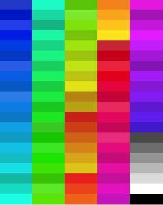
Here is a selection of them, 100 pieces, more clearly:
Here is a selection of them, 100 pieces, more clearly:
What gives us the use of only these colors? Yes, the fact that to fill the area we do not need to change the state of the data bus in the process of filling. It is enough to switch the state of the signal WE and count how many times we have done it. Moreover, we can invert the WE for as long as necessary, the main thing is not less than what is needed to fill the area. It is easy to calculate that once per pixel we need to transfer two data blocks on the bus, then 2 acknowledgments with the signal WE are required. Accordingly, the full screen is necessary (screen_ width * screen_ length * 2) pulses, or 800 * 480 * 2 = 768000.
How easy it is to generate pulses. Of course! You can use a timer. TIM1 in this controller is faster than TIM2-TIM4 timers, because located on the faster APB2 clocking bus. Studies have shown that by turning on the timer in the PWM generator mode with a minimum divider, you can get a fill time of 32 ms! It is clear that the WE signal should be removed from the timer output, for example PA8 (TIM1_CH1).
Can I still increase the fill rate? It turned out yes, just by sending a SYSCLK signal from the RCC_MCO output to the WE LCD input. This is the maximum available frequency on the processor, 72 MHz. The time to fill the display with a symmetrical color is 10.7 ms.
The time is counted by the timer, after which the signal is removed by interruption, and the port switches to the output mode.
Code
// void SSD1963_TimInit2(void){ TIM_TimeBaseInitTypeDef Timer; RCC_APB1PeriphClockCmd(RCC_APB1Periph_TIM4, ENABLE); TIM_TimeBaseStructInit(&Timer); Timer.TIM_Prescaler = 72-1; Timer.TIM_Period = 10000; Timer.TIM_CounterMode = TIM_CounterMode_Down; TIM_TimeBaseInit(TIM4, &Timer); TIM_ITConfig(TIM4, TIM_IT_Update, ENABLE); NVIC_EnableIRQ(TIM4_IRQn); } void SSD1963_WriteDataPix(uint32_t pixdata, uint32_t n){ GPIO_InitTypeDef GPIO_InitStr; SET_LCD_RDS; LCD_DATA_PORT->ODR = (LCD_DATA_PORT->ODR & ~0x01ff) | (pixdata & 0x01ff); GPIO_InitStr.GPIO_Pin = LCD_WR; GPIO_InitStr.GPIO_Mode = GPIO_Mode_AF_PP; GPIO_InitStr.GPIO_Speed = GPIO_Speed_50MHz; GPIO_Init(LCD_WR_PORT, &GPIO_InitStr); // TIM_ITConfig(TIM4, TIM_IT_Update, DISABLE); // if (n > 32000 ){ TIM_PrescalerConfig(TIM4, 72 - 1, TIM_PSCReloadMode_Immediate); // 1 TIM4->CNT = (uint16_t) (n / 36); // } else { TIM_PrescalerConfig(TIM4, 0, TIM_PSCReloadMode_Immediate); // 1/72 () TIM4->CNT = (uint16_t) (n * 2 - 1); // } TIM_ClearITPendingBit(TIM4, TIM_IT_Update); // TIM_ITConfig(TIM4, TIM_IT_Update, ENABLE); // RCC_MCOConfig(RCC_MCO_SYSCLK); //MCO TIM4->CR1 |= TIM_CR1_CEN; // } void TIM4_IRQHandler() { GPIO_InitTypeDef GPIO_InitStr; if (TIM_GetITStatus(TIM4, TIM_IT_Update) != RESET) { TIM_ClearITPendingBit(TIM4, TIM_IT_Update); // TIM_Cmd(TIM4, DISABLE); // RCC_MCOConfig(RCC_MCO_NoClock); // SYSCLK MCO GPIO_InitStr.GPIO_Mode = GPIO_Mode_Out_PP; GPIO_InitStr.GPIO_Speed = GPIO_Speed_50MHz; GPIO_InitStr.GPIO_Pin = LCD_WR; GPIO_Init(LCD_WR_PORT, &GPIO_InitStr); // } } void SSD1963_ClearScreen_9(uint32_t color) { SSD1963_SetArea(0, TFT_WIDTH-1 , 0, TFT_HEIGHT-1); SSD1963_WriteCommand(0x2c); SSD1963_WriteDataPix(color, TFT_HEIGHT*TFT_WIDTH); } int main(void){ tick_init(); // lcd_port_init(); // - SSD1963_Init(); // SSD1963_TimInit2(); // TIM4 SSD1963_ClearScreen_9(0x1ff); // while(1) {} } The timer counts the time with an accuracy of 1/72 µs for the number of points less than 32000 and with an accuracy of 1 µs for more points. This is due to the bit counter timer. Given that it takes some time to process the interrupt when the timer is turned off, the signal at the MCO output is removed a little later than required, with a small margin. It was established experimentally that it is about 10-11 clock speeds of the processor. Thus, we can say that there is a threshold for using this technique, at which it remains faster, despite the overhead of initializing the timer and RCC_MCO and shutting down. A square of 2x2 pixels is probably more profitable to programmatically fill the cycle.
As an output, it can be said that by adding some restrictions, the screen filling time was reduced from 375 to 11 ms. In addition, the filling is without the participation of the processor, which at this time can perform other tasks.
I will be glad comments and additions.
Source: https://habr.com/ru/post/278967/
All Articles