How to parse text with bare hardware, without a processor and without software
Someone is parsing a text file with a program on Python, another is writing a script with regular expressions on Perl, a C programmer bashfully tinkering with buffers and pointers, sometimes using Yacc and Lex.
Is it possible to parse the text with bare iron? No program at all?
“And how is it ?,” a friend asked me, “With the help of Arduino?”
')
“Inside Arduino, there is quite a von Neumann processor and the program works,” I replied. “No, even more bare hardware.”
“Ahhhhhhh, this microcode?” My companion guessed and looked at me triumphantly.
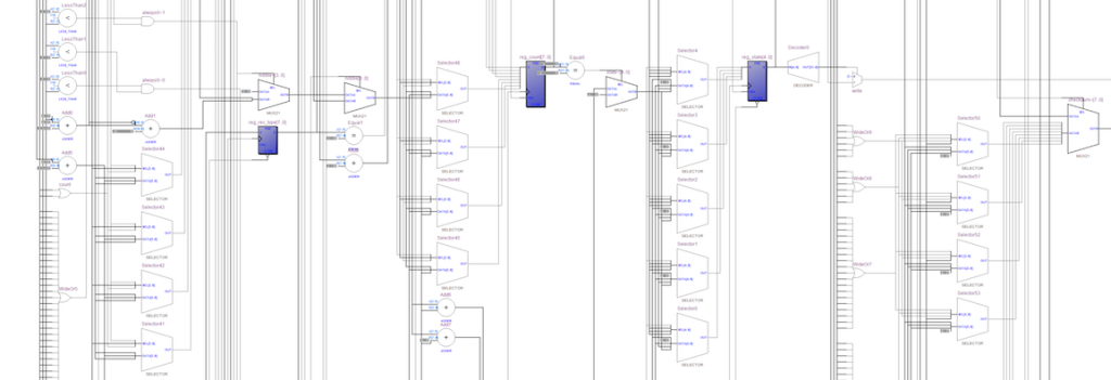
- No, the term "microcode" was used for the specific organization of processors in the 1970s, then its use came to naught, - I answered and added, - Truth, there are still microoperations in Intel processors, into which x86 is recoded, but this is also different . No, I mean text parsing by a device consisting of AND-OR-NOT logical gates and D-triggers, as in the picture below.
- Impossible! - exclaimed my friend, - in such a device somewhere on the side should sit the processor and slyly wink!
“Why is this impossible?” I retorted, “You know the Turing machine?” Parsing text on the tape, and no Intel and arduino at the side wink.
“Well, Turing machine,” drawled his friend, “this is an abstraction, such as Demon Maxwell.”
“No abstraction, now you will see a working scheme parsing the text,” I said, and added, “but first I’ll tell you why I needed it at all.”
Last year, I participated as one of the organizers in a series of seminars on MIPSfpga . MIPSfpga is a package that contains the processor core in the source code on Verilog, which can be changed, add new instructions, build multiprocessor systems, simultaneously change software and hardware, etc. The MIPSfpga system can be simulated in the simulator verilogue, synthesized and implemented on the FPGA board , or with a strong desire to make a chip on it at the factory.
FPGA / FPGA board with MIPSfpga needs to be programmed twice - first fill the PC hardware configuration into it (determine the logical function of each FPGA cell and the connections between them), and then pour the software (processor sequence) into the synthesized hardware memory (also with the PC) systems (which includes the MIPS microAptiv UP processor core, interconnect, two memory blocks and an I / O unit).
There are no problems with uploading a hardware - both Xilinx ISE / Vivado and Altera Quartus II contain software that allows you to upload the hardware configuration to the boards I work with using a simple USB cable without any additions from the user. Such boards include Digilent Basys 3 and Nexys 4 DDR , Terasic DE0-CV and others.
Unlike the hardware configuration, the software in the standard MIPSfpga Getting Started package is poured through the EJTAG debugging interface using an additional fee, called BusBlaster , in combination with the software, which is called OpenOCD . Unfortunately, the BusBlaster / Open OCD combination is quite raw - it may have driver problems in some versions of Windows and Linux. In addition, BusBlaster is nontrivial to buy in Russia. Therefore, before the seminars, I thought about how to fill the software part of the system in MIPSfpga without BusBlaster / OpenOCD.
Software that needs to be uploaded to MIPSfpga is the most common C or assembler program that is compiled and linked by regular GCC to an ELF file. The GNU package also contains the objcopy program, which can turn ELF into a variety of formats, including text-based Intel HEX, Motorola S-record, and a format that the built-in subroutine $ readmemh in the Verilog hardware description language understands. At first I wanted to use the Intel HEX format, but found that it does not support the one of the objcopy options for MIPS that I used. The second option was to use the format
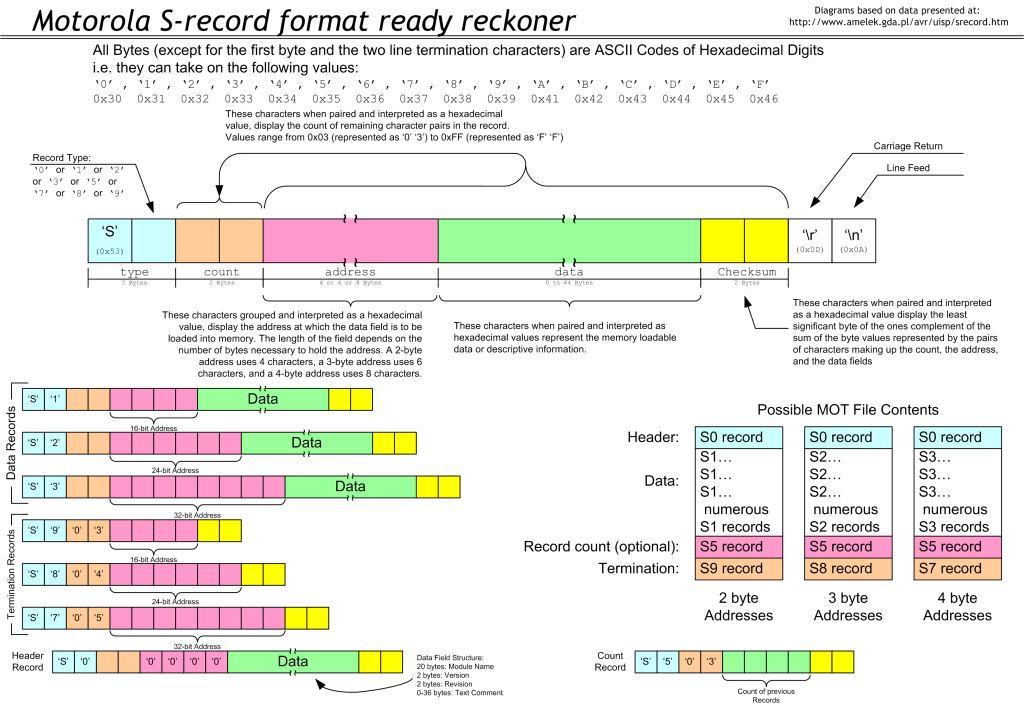
Motorola S-record , and with them everything turned out well. Here is a cheat sheet for this format:
3.1. The easiest way to avoid uploading software through BusBlaster is to simply put it into the MIPSfpga system during its synthesis — a process in which the code in the Verilog hardware description language is converted into a graph from logic elements and triggers. Both the Xilinx ISE / Vivado synthesizer and Altera Quartus II recognize the Verilog $ readmemh structure during the synthesis and create a memory that is initialized with data from a text file . Unfortunately, this solution is very impractical if the user is going to frequently recompile the software, since each time he will also have to re-synthesize the hardware, which can take from 15 to 30 minutes.
3.1.1. Option 3.1 is a partial reconfiguration of the FPGA. I did not investigate it, because I learned that in this case I would have to wait a long time, and I want to wait no more than a few seconds. In addition, I wanted something that did not depend on the manufacturer of FPGAs.
3.2. The most intuitively expected way for embedded programmers is to make part of the program fixed, which is placed into the system during its synthesis (bootloader), and another part of the program is downloaded from the PC via the serial port. The boot program would have to initiate the transfer of the loadable program from the PC, receive this program in the form of data, which is then stored in memory. This method was described by @Frantony in a note on Habré "MIPSfpga: outside the canon"
3.2.1. At method 3.2. There are two variations - transfer the loadable program as a text file in a format like Motorola S-record and parse this file in the bootloader on the board, or, alternatively, parse the text file on the PC and transfer the data to the board in binary form.
3.3. The method that I used - all data reception, parsing and data stuffing from memory is done completely in the hardware implemented in the FPGA. The advantage of this method is that the software on the board is completely unaware of the existence of a hardware downloader. When the hardware loader notices the data coming from the PC, it sets the processor to reset, receives and places all the data in memory, removes the processor from the reset, after which the processor starts reading and executing the reset exception handler code.
3.3.1. In the process of discussing the task with other users and developers, MIPSfpga also expressed the idea of making a full-fledged DMA port for recording data from a PC into memory at the same time as the processor works with the memory (and not when the processor is reset), but it was rejected as too complicated and by and large meaningless for the types of tasks in which it was supposed to use MIPSfpga during seminars in Russia.
The serial port is a very old invention. UART / RS-232C appeared in the late 1960s. All PCs in the 1980s were with COM ports that could be written as to a file. You will not believe it, but it has survived MS-DOS and has remained in Windows so far. Yes, yes, in order to transfer a file from a PC to an external serial port, you can now write “type COM file-name COM -port number ” on the command line:

In Linux, there is also such a connection (although I have not tried MIPSfpga connected to Linux yet, but it was tried by a friend in Italy who sent me an email about it). The Linux user who copies the data to the file corresponding to the COM port should belong to the dialup group:
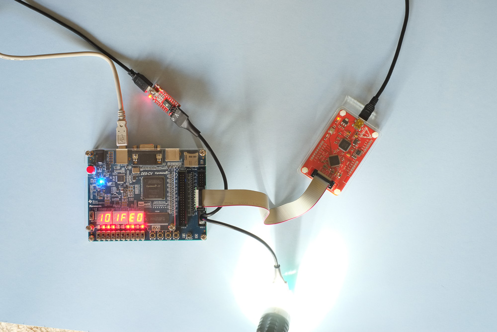
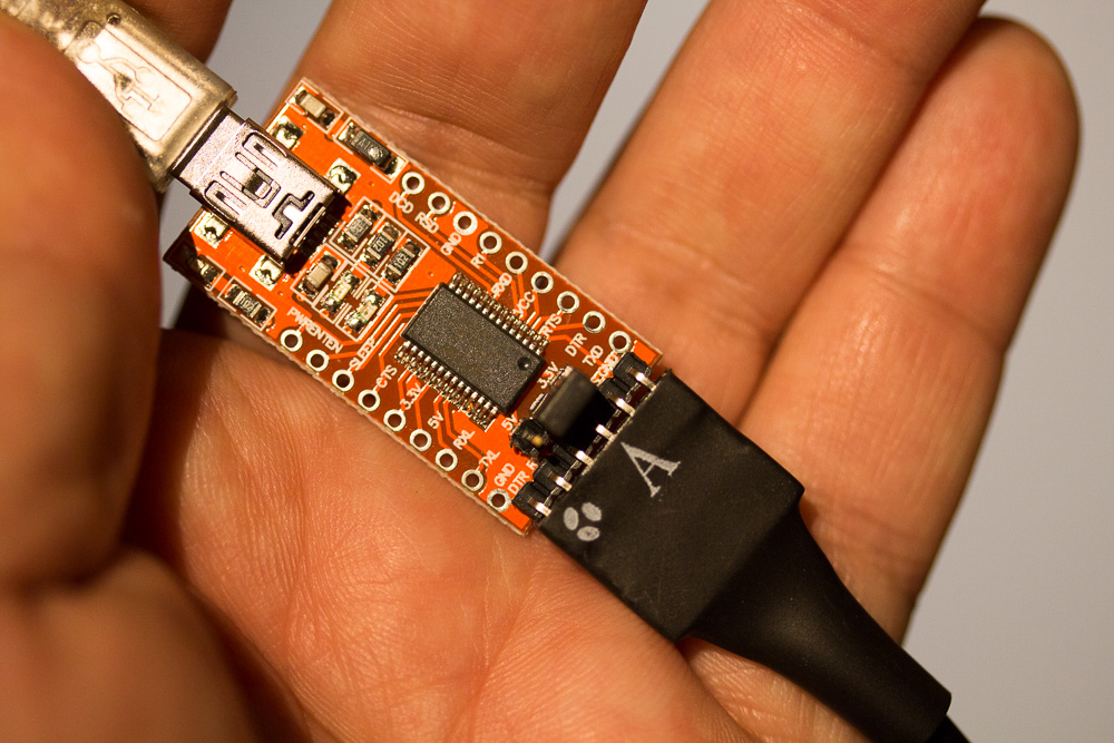
At the same time, the ancient RS-232C ports in modern PCs are not installed, instead they make a “virtual COM port” via USB, using this FTD32RL chip adapter from the FTDI company (Attention! This chip has many buggy fakes ) I also pay attention that for working with FPGA the 3.3 / 5V switch on the adapter should be set to 3.3V, otherwise theoretically it is possible to damage the pins / pins of the FPGA, which are usually softer than, for example, microcontrollers:
In addition to the adapter shown in the photo above, you can use a cable called PL2303TA USB TTL to RS232 Converter XP / VISTA / 7/8 / 8.1 for connecting the PC and UART to the FPGA. This cable is useful for small Terasic DE0-Nano boards with male GPIO pins. On sites like AliExpress, a cheaper cable based on the PL2303HX chip is also being sold, but this chip had some compatibility issues with Windows 8.x, so it's better to use a cable based on the PL2303TA (UPD: I changed the latest version of MIPSfpga + the used pins for the DE0-Nano board, so this snapshot needs to be replaced, the connection in it is not true):

Before I inserted the modules of the downloadable program from the PC into the memory of the synthesized system MIPSfpga + (as I called my version MIPSfpga), its modular hierarchy looked like this:

What is in each module:
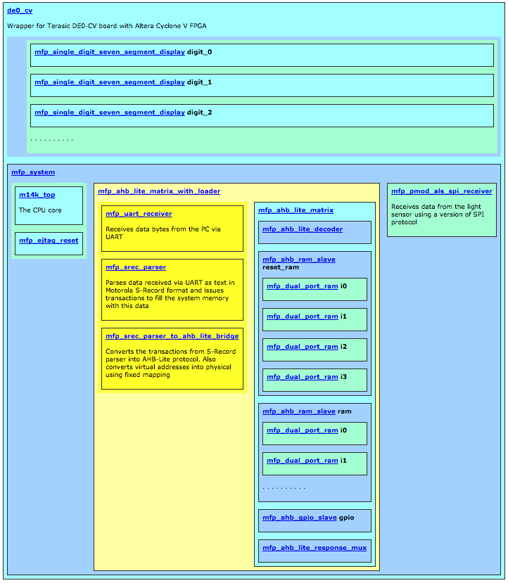
Four new modules:
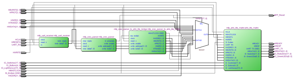
Below is the scheme at the hierarchy level of the mfp_ahb_lite_matrix_with_loader module, obtained after compiling the code on the verification, but before complete synthesis (optimization, mapping to FPGA-specific elements, placement and tracing). Pay attention to the multiplexer between mfp_srec_parser_to_ahb_lite_bridge and mfp_ahb_lite_matrix , it sends to the memory and I / O subsystem transactions from the microprocessor core, or transactions from the hardware loader:
The UART topic has been discussed on Habré many times, including quite recently , so I will not dwell on it in detail. My receiver implementation uses the simplest version of the UART protocol , without control signals, with one leading bit, without parity checks, with a fixed transmission rate and for a fixed clock / clock frequency. The mfp_uart_receiver module receives data from the RX signal sequentially and outputs an 8-bit byte in parallel when it is ready. The module contains a finite state machine, which waits for a negative edge of the RX signal (thus determining the initial bit), and then reads the data bits at the correct times, which are determined by counting clock cycles using a counter. Since the number of clock cycles per bit is rather large, 50,000,000 Hz / 115,200 baud = 434 clock cycles (or 217 clock cycles for 25 MHz), data reception is fairly reliable. Here is the module interface:

The full code of the module is http://github.com/MIPSfpga/mipsfpga-plus/blob/master/mfp_uart_receiver.v .
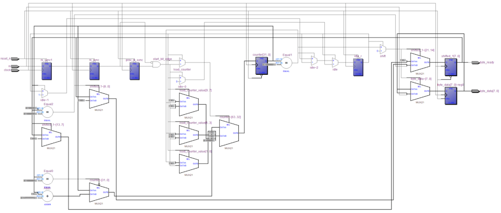
Scheme of the mfp_uart_receiver module after initial compilation:
The mfp_srec_parser module receives the bytes from the mfp_uart_receiver module and parses them as text in a Motorola S-record format using a state machine. During parsing, the formation of transactions to the memory of the synthesized system MIPSfpga + also takes place; these transactions fill the memory with the bytes specified from the parsed text at the addresses specified in the text. Module Interface:

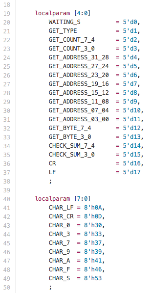
We determine the identifiers of constants for the states of the finite state machine and the ASCII symbols used:
Combination logic for converting the character constants '0', '1', ... '9', 'A', 'B', ... 'F' into four-bit numbers 0, 1, 2, ... 9, 10, 11, ... 15.

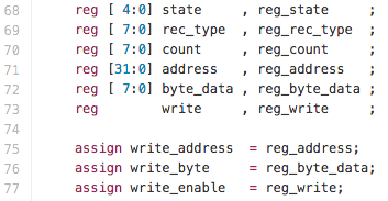
Variables for the state machine. On the left - the new value created in the current cycle / cycle, on the right - the value recorded in the register / D-flip-flop / D-flip-flop, formed in the previous cycle. I note that the synthesizer doesn’t always make a D-flip-flop / register from the verilog “reg” in the hardware sense. The key word “reg” should be perceived only as a kind of variable that can be assigned to assignments inside the “always” -blocks:
Assignments after defining variables are assignments to the module outputs of the generated addresses (which are previously written to the registers):
The logic of a finite state machine consists of a combination part and a sequence part. If you are not familiar with these concepts, you can read them in the free Harris & Harris tutorial.
In the combinational part, we calculate the values for the next state, and the word “state” means not only the group of D-flip-flops, into which the reg_state variable turns , but generally all D-flip-flops / D-flip-flop / hardware registers in the scheme (all three terms in the context of this post are interchangeable). There are purists who say that this is a “finite automaton,” and a “finite automaton with data,” but we will leave these scholastics and their devils on the tip of the needle alone.
Here is the beginning of the combination part. In order not to follow the appearance of latches (D-latch) that are undesirable in the synchronous design methodology, we will assign a default value to all calculated variables at the very beginning of the always-combinational block:

Any changes occur only when we receive a new letter from the UART receiver (“if (char_ready)”). In our finite state machine, we first wait for the appearance of the letter 'S', after which we parse the record type (we are interested in the type '3') and the address at which we will write the next bytes:
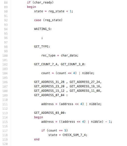
Now we begin to parse the data and at the same time generate the address / data transaction to the output from the module:

On the positive front of the clock signal generator, write the previously calculated values to the registers that do not require a reset:

And now we make an entry in the registers that require a reset — either to start the operation of the state machine with an unambiguous state, or registers that define control signals at the output of the module:

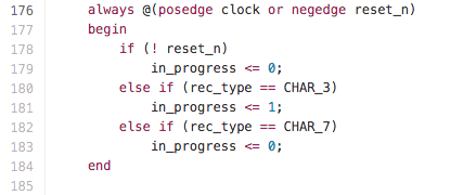
The in_progress signal (“in progress”) has been enabled since the recognition of the first entry with the address (type S3 ) and turned off when the module recognizes the last entry in the file (type S7 ). This signal can be output to an external indicator on the board, it is also used for the multiplexer in mfp_ahb_lite_matrix_with_loader and determines whether the microprocessor core or the hardware loader writes to memory. In addition, in_progress is used to reset the microprocessor core, so that it is "cut down" while the hardware loader writes to memory. When the software is stored in memory, the microprocessor “wakes up” and starts reading instructions (from the fixed physical address 1FC0_0000).
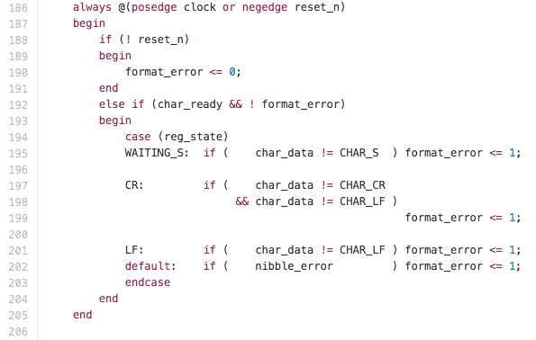
Logic for detecting errors in the input text. It works in parallel with the main state machine and uses its states:
Logic for calculating checksums and comparing them with checksums from S-Record text. It works in parallel with the main state machine and uses its states:

Generate error signal. The hardware parser even tells the user which line the error occurred on:

The full code of the module is http://github.com/MIPSfpga/mipsfpga-plus/blob/master/mfp_srec_parser.v
The mfp_srec_parser_to_ahb_lite_bridge module turns address / data translations obtained from the mfp_srec_parser module into a transaction for the AHB-Lite bus that MIPSfpga uses.
The module also edits addresses - turns the virtual addresses that the software uses into physical addresses that the hardware uses. Although the MIPS microAptiv UP processor has a MMU TLB that allows flexible and complex mapping of virtual addresses to physical ones, but in my examples of using MIPSfpga, the conversion is simple and fixed - simply zeroing the three upper bits of the address. If you are interested in the work of the virtual memory management device in MIPSfpga, you can watch the presentation in Russian “Memory management device in MIPS processors” .
Bridge code mfp_srec_parser_to_ahb_lite_bridge :
http://github.com/MIPSfpga/mipsfpga-plus/blob/master/mfp_srec_parser_to_ahb_lite_bridge.v

Scheme of the mfp_srec_parser_to_ahb_lite_bridge module after the initial compilation:
And finally, about the AHB-Lite bus itself, which is used to connect devices in systems on a chip.
Below is an excerpt from the documentation from Imagination Technologies, which can be downloaded using the following instructions .

In particular, you can see why data transfer has to be delayed by one cycle in relation to the transmission of an address. In the AHB-Lite protocol, the new transaction address is laid out on the bus simultaneously with the data from the previous transaction:

Diagram of the mfp_ahb_lite_matrix module after the initial compilation. This module contains three slave modules — two memory blocks and a module that displays the software’s memory access to general-purpose I / O — GPIO (General Purpose IO):
In this post, I described only one aspect of the MIPSfpga project and its improvement, MIPSfpga +, which I did not have to worry about the problems of Bus Blaster / Open OCD during my trip to Russia at the end of last year. Note that if you want to use a GDB-based debugger with MIPSfpga, then you will still have to use Bus Blaster or another debugging adapter that supports EJTAG.
But the MIPSfpga theme is much more. After all, the package contains an industrial processor, which is used in new products from Samsung, Microchip and other companies - and you, dear readers, can experiment with its structure, using the same code that is used by the engineers in these companies. You can write your own cache module with a different row push policy, develop multi-core systems, attach various peripherals to MIPSfpga. If you are interested in making a project with MIPSfpga and you are working at some provincial university, which is difficult to get the budget for purchasing FPGA boards, you can get one board for free, though there are few of them left - see “Distribution of elephants: FPGA boards for educational projects with MIPSfpga . "
Also on Habré, there was already a note about how to tie a coprocessor to the MIPSfpga - see https://habrahabr.ru/post/276205/ .
Is it possible to parse the text with bare iron? No program at all?
“And how is it ?,” a friend asked me, “With the help of Arduino?”
')
“Inside Arduino, there is quite a von Neumann processor and the program works,” I replied. “No, even more bare hardware.”
“Ahhhhhhh, this microcode?” My companion guessed and looked at me triumphantly.
- No, the term "microcode" was used for the specific organization of processors in the 1970s, then its use came to naught, - I answered and added, - Truth, there are still microoperations in Intel processors, into which x86 is recoded, but this is also different . No, I mean text parsing by a device consisting of AND-OR-NOT logical gates and D-triggers, as in the picture below.
- Impossible! - exclaimed my friend, - in such a device somewhere on the side should sit the processor and slyly wink!
“Why is this impossible?” I retorted, “You know the Turing machine?” Parsing text on the tape, and no Intel and arduino at the side wink.
“Well, Turing machine,” drawled his friend, “this is an abstraction, such as Demon Maxwell.”
“No abstraction, now you will see a working scheme parsing the text,” I said, and added, “but first I’ll tell you why I needed it at all.”
1. Why did I need to parse the text with a hardware without software
Last year, I participated as one of the organizers in a series of seminars on MIPSfpga . MIPSfpga is a package that contains the processor core in the source code on Verilog, which can be changed, add new instructions, build multiprocessor systems, simultaneously change software and hardware, etc. The MIPSfpga system can be simulated in the simulator verilogue, synthesized and implemented on the FPGA board , or with a strong desire to make a chip on it at the factory.
FPGA / FPGA board with MIPSfpga needs to be programmed twice - first fill the PC hardware configuration into it (determine the logical function of each FPGA cell and the connections between them), and then pour the software (processor sequence) into the synthesized hardware memory (also with the PC) systems (which includes the MIPS microAptiv UP processor core, interconnect, two memory blocks and an I / O unit).
There are no problems with uploading a hardware - both Xilinx ISE / Vivado and Altera Quartus II contain software that allows you to upload the hardware configuration to the boards I work with using a simple USB cable without any additions from the user. Such boards include Digilent Basys 3 and Nexys 4 DDR , Terasic DE0-CV and others.
Unlike the hardware configuration, the software in the standard MIPSfpga Getting Started package is poured through the EJTAG debugging interface using an additional fee, called BusBlaster , in combination with the software, which is called OpenOCD . Unfortunately, the BusBlaster / Open OCD combination is quite raw - it may have driver problems in some versions of Windows and Linux. In addition, BusBlaster is nontrivial to buy in Russia. Therefore, before the seminars, I thought about how to fill the software part of the system in MIPSfpga without BusBlaster / OpenOCD.
2. Which file you need to parse and upload to the system’s memory
Software that needs to be uploaded to MIPSfpga is the most common C or assembler program that is compiled and linked by regular GCC to an ELF file. The GNU package also contains the objcopy program, which can turn ELF into a variety of formats, including text-based Intel HEX, Motorola S-record, and a format that the built-in subroutine $ readmemh in the Verilog hardware description language understands. At first I wanted to use the Intel HEX format, but found that it does not support the one of the objcopy options for MIPS that I used. The second option was to use the format
Motorola S-record , and with them everything turned out well. Here is a cheat sheet for this format:
3. How to fill and how - engineering solutions options
3.1. The easiest way to avoid uploading software through BusBlaster is to simply put it into the MIPSfpga system during its synthesis — a process in which the code in the Verilog hardware description language is converted into a graph from logic elements and triggers. Both the Xilinx ISE / Vivado synthesizer and Altera Quartus II recognize the Verilog $ readmemh structure during the synthesis and create a memory that is initialized with data from a text file . Unfortunately, this solution is very impractical if the user is going to frequently recompile the software, since each time he will also have to re-synthesize the hardware, which can take from 15 to 30 minutes.
3.1.1. Option 3.1 is a partial reconfiguration of the FPGA. I did not investigate it, because I learned that in this case I would have to wait a long time, and I want to wait no more than a few seconds. In addition, I wanted something that did not depend on the manufacturer of FPGAs.
3.2. The most intuitively expected way for embedded programmers is to make part of the program fixed, which is placed into the system during its synthesis (bootloader), and another part of the program is downloaded from the PC via the serial port. The boot program would have to initiate the transfer of the loadable program from the PC, receive this program in the form of data, which is then stored in memory. This method was described by @Frantony in a note on Habré "MIPSfpga: outside the canon"
3.2.1. At method 3.2. There are two variations - transfer the loadable program as a text file in a format like Motorola S-record and parse this file in the bootloader on the board, or, alternatively, parse the text file on the PC and transfer the data to the board in binary form.
3.3. The method that I used - all data reception, parsing and data stuffing from memory is done completely in the hardware implemented in the FPGA. The advantage of this method is that the software on the board is completely unaware of the existence of a hardware downloader. When the hardware loader notices the data coming from the PC, it sets the processor to reset, receives and places all the data in memory, removes the processor from the reset, after which the processor starts reading and executing the reset exception handler code.
3.3.1. In the process of discussing the task with other users and developers, MIPSfpga also expressed the idea of making a full-fledged DMA port for recording data from a PC into memory at the same time as the processor works with the memory (and not when the processor is reset), but it was rejected as too complicated and by and large meaningless for the types of tasks in which it was supposed to use MIPSfpga during seminars in Russia.
4. How is the connection to the PC?
The serial port is a very old invention. UART / RS-232C appeared in the late 1960s. All PCs in the 1980s were with COM ports that could be written as to a file. You will not believe it, but it has survived MS-DOS and has remained in Windows so far. Yes, yes, in order to transfer a file from a PC to an external serial port, you can now write “type COM file-name COM -port number ” on the command line:
In Linux, there is also such a connection (although I have not tried MIPSfpga connected to Linux yet, but it was tried by a friend in Italy who sent me an email about it). The Linux user who copies the data to the file corresponding to the COM port should belong to the dialup group:
 stty -F / dev / ttyUSB0 raw 115200
 cat srec program.rec> / dev / ttyUSB0
At the same time, the ancient RS-232C ports in modern PCs are not installed, instead they make a “virtual COM port” via USB, using this FTD32RL chip adapter from the FTDI company (Attention! This chip has many buggy fakes ) I also pay attention that for working with FPGA the 3.3 / 5V switch on the adapter should be set to 3.3V, otherwise theoretically it is possible to damage the pins / pins of the FPGA, which are usually softer than, for example, microcontrollers:
In addition to the adapter shown in the photo above, you can use a cable called PL2303TA USB TTL to RS232 Converter XP / VISTA / 7/8 / 8.1 for connecting the PC and UART to the FPGA. This cable is useful for small Terasic DE0-Nano boards with male GPIO pins. On sites like AliExpress, a cheaper cable based on the PL2303HX chip is also being sold, but this chip had some compatibility issues with Windows 8.x, so it's better to use a cable based on the PL2303TA (UPD: I changed the latest version of MIPSfpga + the used pins for the DE0-Nano board, so this snapshot needs to be replaced, the connection in it is not true):
5. Where did the data from the PC need to be uploaded?
Before I inserted the modules of the downloadable program from the PC into the memory of the synthesized system MIPSfpga + (as I called my version MIPSfpga), its modular hierarchy looked like this:
What is in each module:
- de0_cv is an external module specific to each type of FPGA board. The findings of this module correspond to the physical findings on the chip itself. The specific module de0_cv is written for the Terasic DE0-CV board with FPGA Altera Cyclone V
- mfp_single_digit_seven_segment_display display_0, display_1, ... - seven-segment indicator drivers for Alter cards (one per digit)
- mfp_system - system module, the same for all FPGA boards
- m14k_top is the upper module of the microprocessor core MIPS microAptiv UP (also called MIPS microAptiv MPU) , the name m14k remains from the previous processor version - MIPS M14Kc
- mfp_ejtag_reset - auxiliary module for resetting the EJTAG debugging interface
- mfp_ahb_lite_matrix is a module that combines memory blocks, a circuit implementation of AHB-Lite bus logic, and I / O logic. The latter links the addresses on the bus coming from the software with the signals of the hardware I / O devices — buttons, LED indicators, etc.
- mfp_ahb_lite_decoder - the module that decodes the address on the AHB-Lite bus and determines which of the slaves (memory blocks or the I / O logic module) should process the transaction on the bus
- mfp_ahb_ram_slave reset_ram is a memory block shell that implements the AHB-Lite bus slave protocol. This group of blocks ( reset_ram ) is intended for the part of the program that starts immediately after the processor leaves the reset state.
- mfp_dual_port_ram i0-i3 - modules, the code on the chain in which the synthesizer recognizes as an indication to create a block memory inside the FPGA. In order for the synthesizer to correctly perceive this code, it must be written in a certain way . Four blocks with 8-bit memory width (instead of 1 block of 32-bits width) so that you can record one byte from the 4-byte AHB-Lite bus (the synthesizer does not understand the masked memory)
- mfp_ahb_ram_slave ram is another shell of memory blocks that implements the protocol of the AHB-Lite bus slave. This group of blocks ( ram ) is intended for the main part of the program that runs on cached memory.
- mfp_dual_port_ram i0-i3 - see the same four blocks above
- mfp_ahb_gpio_slave - module of the slave device for general purpose input-output (GPIO - General Purpose Input / Output). Displays the addresses on the bus, coming from the software to the signals of the hardware input-output devices - buttons, LED-indicators, etc.
- mfp_ahb_lite_response_mux - auxiliary module for AHB-Lite bus operation - multiplexer to send read data from the correct memory block or I / O module to the master device (microprocessor core)
- mfp_pmod_als_spi_receiver is a module that implements a variant of the SPI protocol for the Digilent PmodALS light sensor , one of the examples of devices connected to the MIPSfpga + system. In this post, this module is not discussed, I may write a separate post about the integration of the light sensor with MIPSfpga +
6. How did the system hierarchy change when I inserted a hardware loader into it?
Four new modules:
- mfp_ahb_lite_matrix_with_loader - is put in place of the mfp_ahb_lite_matrix module from the previous hierarchy. mfp_ahb_lite_matrix_with_loader contains both the mfp_ahb_lite_matrix module and three modules with new functionality:
- mfp_uart_receiver - receives data from PC via UART and turns it into a stream of bytes / alphanumeric characters
- mfp_srec_parser - parses the chain of bytes received from the mfp_uart_receiver module as text in the Motorola S-Record format and generates a sequence of translations (address / data) to fill the memory of the synthesized system with the data specified in the text
- mfp_srec_parser_to_ahb_lite_bridge - converts transactions received from the mfp_srec_parser module into transactions that comply with the AHB-Lite bus protocol. It also turns the virtual addresses that the software uses into physical addresses that the hardware uses, using a simple fixed mapping.
Below is the scheme at the hierarchy level of the mfp_ahb_lite_matrix_with_loader module, obtained after compiling the code on the verification, but before complete synthesis (optimization, mapping to FPGA-specific elements, placement and tracing). Pay attention to the multiplexer between mfp_srec_parser_to_ahb_lite_bridge and mfp_ahb_lite_matrix , it sends to the memory and I / O subsystem transactions from the microprocessor core, or transactions from the hardware loader:
7. A few words about the serial port, UART
The UART topic has been discussed on Habré many times, including quite recently , so I will not dwell on it in detail. My receiver implementation uses the simplest version of the UART protocol , without control signals, with one leading bit, without parity checks, with a fixed transmission rate and for a fixed clock / clock frequency. The mfp_uart_receiver module receives data from the RX signal sequentially and outputs an 8-bit byte in parallel when it is ready. The module contains a finite state machine, which waits for a negative edge of the RX signal (thus determining the initial bit), and then reads the data bits at the correct times, which are determined by counting clock cycles using a counter. Since the number of clock cycles per bit is rather large, 50,000,000 Hz / 115,200 baud = 434 clock cycles (or 217 clock cycles for 25 MHz), data reception is fairly reliable. Here is the module interface:
The full code of the module is http://github.com/MIPSfpga/mipsfpga-plus/blob/master/mfp_uart_receiver.v .
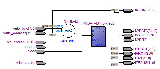
Scheme of the mfp_uart_receiver module after initial compilation:
8. And finally, the promised: parser text in the format of Motorola S-Record naked hardware, without a processor and without software
The mfp_srec_parser module receives the bytes from the mfp_uart_receiver module and parses them as text in a Motorola S-record format using a state machine. During parsing, the formation of transactions to the memory of the synthesized system MIPSfpga + also takes place; these transactions fill the memory with the bytes specified from the parsed text at the addresses specified in the text. Module Interface:
We determine the identifiers of constants for the states of the finite state machine and the ASCII symbols used:
Combination logic for converting the character constants '0', '1', ... '9', 'A', 'B', ... 'F' into four-bit numbers 0, 1, 2, ... 9, 10, 11, ... 15.
Variables for the state machine. On the left - the new value created in the current cycle / cycle, on the right - the value recorded in the register / D-flip-flop / D-flip-flop, formed in the previous cycle. I note that the synthesizer doesn’t always make a D-flip-flop / register from the verilog “reg” in the hardware sense. The key word “reg” should be perceived only as a kind of variable that can be assigned to assignments inside the “always” -blocks:
Assignments after defining variables are assignments to the module outputs of the generated addresses (which are previously written to the registers):
The logic of a finite state machine consists of a combination part and a sequence part. If you are not familiar with these concepts, you can read them in the free Harris & Harris tutorial.
In the combinational part, we calculate the values for the next state, and the word “state” means not only the group of D-flip-flops, into which the reg_state variable turns , but generally all D-flip-flops / D-flip-flop / hardware registers in the scheme (all three terms in the context of this post are interchangeable). There are purists who say that this is a “finite automaton,” and a “finite automaton with data,” but we will leave these scholastics and their devils on the tip of the needle alone.
Here is the beginning of the combination part. In order not to follow the appearance of latches (D-latch) that are undesirable in the synchronous design methodology, we will assign a default value to all calculated variables at the very beginning of the always-combinational block:
Any changes occur only when we receive a new letter from the UART receiver (“if (char_ready)”). In our finite state machine, we first wait for the appearance of the letter 'S', after which we parse the record type (we are interested in the type '3') and the address at which we will write the next bytes:
Now we begin to parse the data and at the same time generate the address / data transaction to the output from the module:
On the positive front of the clock signal generator, write the previously calculated values to the registers that do not require a reset:
And now we make an entry in the registers that require a reset — either to start the operation of the state machine with an unambiguous state, or registers that define control signals at the output of the module:
The in_progress signal (“in progress”) has been enabled since the recognition of the first entry with the address (type S3 ) and turned off when the module recognizes the last entry in the file (type S7 ). This signal can be output to an external indicator on the board, it is also used for the multiplexer in mfp_ahb_lite_matrix_with_loader and determines whether the microprocessor core or the hardware loader writes to memory. In addition, in_progress is used to reset the microprocessor core, so that it is "cut down" while the hardware loader writes to memory. When the software is stored in memory, the microprocessor “wakes up” and starts reading instructions (from the fixed physical address 1FC0_0000).
Logic for detecting errors in the input text. It works in parallel with the main state machine and uses its states:
Logic for calculating checksums and comparing them with checksums from S-Record text. It works in parallel with the main state machine and uses its states:
Generate error signal. The hardware parser even tells the user which line the error occurred on:
The full code of the module is http://github.com/MIPSfpga/mipsfpga-plus/blob/master/mfp_srec_parser.v
9. A few words about the bridge to the bus AHB-Lite
The mfp_srec_parser_to_ahb_lite_bridge module turns address / data translations obtained from the mfp_srec_parser module into a transaction for the AHB-Lite bus that MIPSfpga uses.
The module also edits addresses - turns the virtual addresses that the software uses into physical addresses that the hardware uses. Although the MIPS microAptiv UP processor has a MMU TLB that allows flexible and complex mapping of virtual addresses to physical ones, but in my examples of using MIPSfpga, the conversion is simple and fixed - simply zeroing the three upper bits of the address. If you are interested in the work of the virtual memory management device in MIPSfpga, you can watch the presentation in Russian “Memory management device in MIPS processors” .
Bridge code mfp_srec_parser_to_ahb_lite_bridge :
http://github.com/MIPSfpga/mipsfpga-plus/blob/master/mfp_srec_parser_to_ahb_lite_bridge.v
Scheme of the mfp_srec_parser_to_ahb_lite_bridge module after the initial compilation:
And finally, about the AHB-Lite bus itself, which is used to connect devices in systems on a chip.
Below is an excerpt from the documentation from Imagination Technologies, which can be downloaded using the following instructions .
In particular, you can see why data transfer has to be delayed by one cycle in relation to the transmission of an address. In the AHB-Lite protocol, the new transaction address is laid out on the bus simultaneously with the data from the previous transaction:
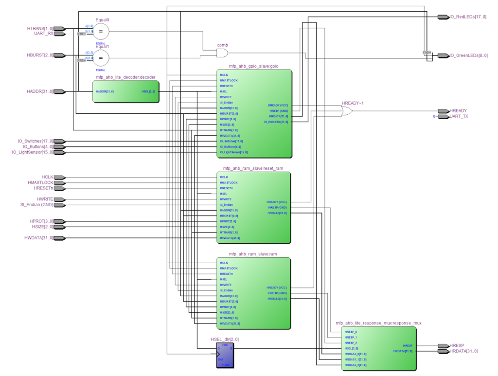
Diagram of the mfp_ahb_lite_matrix module after the initial compilation. This module contains three slave modules — two memory blocks and a module that displays the software’s memory access to general-purpose I / O — GPIO (General Purpose IO):
10. And now what? Proceedings, additions and suggestions
In this post, I described only one aspect of the MIPSfpga project and its improvement, MIPSfpga +, which I did not have to worry about the problems of Bus Blaster / Open OCD during my trip to Russia at the end of last year. Note that if you want to use a GDB-based debugger with MIPSfpga, then you will still have to use Bus Blaster or another debugging adapter that supports EJTAG.
But the MIPSfpga theme is much more. After all, the package contains an industrial processor, which is used in new products from Samsung, Microchip and other companies - and you, dear readers, can experiment with its structure, using the same code that is used by the engineers in these companies. You can write your own cache module with a different row push policy, develop multi-core systems, attach various peripherals to MIPSfpga. If you are interested in making a project with MIPSfpga and you are working at some provincial university, which is difficult to get the budget for purchasing FPGA boards, you can get one board for free, though there are few of them left - see “Distribution of elephants: FPGA boards for educational projects with MIPSfpga . "
Also on Habré, there was already a note about how to tie a coprocessor to the MIPSfpga - see https://habrahabr.ru/post/276205/ .
Source: https://habr.com/ru/post/278681/
All Articles