Implementing a stable UART, at a speed of 921600 baud or more, in Verilog language under FPGA
Hello. A couple of weeks ago, I started slowly learning programming for FPGAs. For this purpose, I ordered the cheapest motherboard based on the Altera Max II EPM240T100C5N chip from the Chinese. Having established Quartus v15, began to study Verilog of the standard of 2001. Blinking LEDs decided to try to implement some data transfer protocol. Naturally, it became UART :) Looking at other people's examples on the network, I didn’t really like the excessive piling up of logic, a lot of additional counters, and most importantly, problems with synchronization in the receiver and, as a result, not stability at high speeds. Of course, you can find high-quality implementations that are fully configurable, and indeed, with “ideal code”, but there will not be any sports interest.
And so, the task was to implement the most compact, stable and simple 8-bit asynchronous transceiver with the 1st start and 1st stop bits. In a word - a classic. But as it turned out, the task is not so trivial as it was at first glance. Having realized the receiver and the transmitter literally in one evening, I had to spend two more to make the logic of the chip not swallow, to receive and send the stream of bytes correctly, without errors.
Based on the criticism and wishes in the comments, I have worked on errors, and the article already presents the second implementation of this module. Receiving and sending data were transferred to shift registers, a majority scheme was added to the RX input of three elements, got rid of blocking assignments in synchronous blocks and counters of the UART clock signal count from the maximum value to zero.
')

Project files:
- Main
- UART
- UART_TX
- UART_RX
- Rxmajority3filter
Let's start with the UART_TX module:
UART_TX.v
module UART_TX # ( parameter CLOCK_FREQUENCY = 50_000_000, parameter BAUD_RATE = 9600 ) ( input clockIN, input nTxResetIN, input [7:0] txDataIN, input txLoadIN, output wire txIdleOUT, output wire txReadyOUT, output wire txOUT ); localparam HALF_BAUD_CLK_REG_VALUE = (CLOCK_FREQUENCY / BAUD_RATE / 2 - 1); localparam HALF_BAUD_CLK_REG_SIZE = $clog2(HALF_BAUD_CLK_REG_VALUE); reg [HALF_BAUD_CLK_REG_SIZE-1:0] txClkCounter = 0; reg txBaudClk = 1'b0; reg [9:0] txReg = 10'h001; reg [3:0] txCounter = 4'h0; assign txReadyOUT = !txCounter[3:1]; assign txIdleOUT = txReadyOUT & (~txCounter[0]); assign txOUT = txReg[0]; always @(posedge clockIN) begin : tx_clock_generate if(txIdleOUT & (~txLoadIN)) begin txClkCounter <= 0; txBaudClk <= 1'b0; end else if(txClkCounter == 0) begin txClkCounter <= HALF_BAUD_CLK_REG_VALUE; txBaudClk <= ~txBaudClk; end else begin txClkCounter <= txClkCounter - 1'b1; end end always @(posedge txBaudClk or negedge nTxResetIN) begin : tx_transmit if(~nTxResetIN) begin txCounter <= 4'h0; txReg[0] <= 1'b1; end else if(~txReadyOUT) begin txReg <= {1'b0, txReg[9:1]}; txCounter <= txCounter - 1'b1; end else if(txLoadIN) begin txReg <= {1'b1, txDataIN[7:0], 1'b0}; txCounter <= 4'hA; end else begin txCounter <= 4'h0; end end endmodule Let's sort everything in order:
module UART_TX # ( parameter CLOCK_FREQUENCY = 50_000_000, parameter BAUD_RATE = 9600 ) ( input clockIN, input nTxResetIN, input [7:0] txDataIN, input txLoadIN, output wire txIdleOUT, output wire txReadyOUT, output wire txOUT ); The parameters CLOCK_FREQUENCY and BAUD_RATE are the frequency of the crystal oscillator and the frequency UART of the transmitter, respectively.
Incoming ports:
clockIN is the clock signal port from the quartz resonator.
nTxResetIN - port of discharge on a negative front.
txDataIN is an eight-bit data bus.
txLoadIN - the port of the beginning of data transfer.
Outgoing ports:
txIdleOUT - the transmitter “idle” port, is set in the log. 1 at full completion of the data byte transfer cycle, if there is no log on the txLoadIN port. one.
txReadyOUT - port, log. 1 on which, will mean that the stop bit has been sent, and you can upload new data.
txOUT is a port for serial transmission of outgoing data that must be assigned to the FPGA leg.
localparam HALF_BAUD_CLK_REG_VALUE = (CLOCK_FREQUENCY / BAUD_RATE / 2 - 1); localparam HALF_BAUD_CLK_REG_SIZE = $clog2(HALF_BAUD_CLK_REG_VALUE); reg [HALF_BAUD_CLK_REG_SIZE-1:0] txClkCounter = 0; reg txBaudClk = 1'b0; reg [9:0] txReg = 10'h001; reg [3:0] txCounter = 4'h0; assign txReadyOUT = !txCounter[3:1]; assign txIdleOUT = txReadyOUT & (~txCounter[0]); assign txOUT = txReg[0]; The local parameter HALF_BAUD_CLK_REG_VALUE is the value of the counter-divider of the half-cycle frequency of the UART clock signal. Calculated by the formula CLOCK_FREQUENCY / BAUD_RATE / 2 - 1 .
The local parameter HALF_BAUD_CLK_REG_SIZE is the width of this counter itself. It is calculated by the wonderful function $ clog2 - the logarithm of base 2 from the value of the parameter HALF_BAUD_CLK_REG_VALUE .
Reg registers:
txClkCounter is a clock frequency divider counter.
txBaudClk - clock signal for the transmitter.
txReg - shift register in which the data byte, start and stop bits will be written.
txCounter - the number of bits sent.
Wires wire:
txReadyOUT is assigned as a continuous connection through logical negation on the 4th, 3rd and 2nd bits of the register. txCounter Accepts the state of the log. 1 when txCounter reaches 1 or 0.
txIdleOUT is assigned as a continuous connection to txReadyOUT and through the logical AND primitive to the inverted 1st bit of the txCounter register. Accepts the state log. 1 when the txCounter reaches 0.
txOUT is assigned by continuous connection to the 1st bit of the txReg register
Data transfer:
always @(posedge txBaudClk or negedge nTxResetIN) begin : tx_transmit if(~nTxResetIN) begin txCounter <= 4'h0; txReg[0] <= 1'b1; end else if(~txReadyOUT) begin txReg <= {1'b0, txReg[9:1]}; txCounter <= txCounter - 1'b1; end else if(txLoadIN) begin txReg <= {1'b1, txDataIN[7:0], 1'b0}; txCounter <= 4'hA; end else begin txCounter <= 4'h0; end end On the negative edge on the nTxResetIN port, which is checked in the first condition, a log is set on the first bit of the txReg register. 1, and the txCounter register takes the value 0, which gives the txIdleOUT and txReadyOUT and txOUT log outputs . one.
Otherwise, a positive edge at the txBaudClk port is used to check the signal value of the txReadyOUT port, and, for log. 0, the contents of the txReg register are shifted towards the lower bits, and the txCounter counter is decremented by one, and when the value 1 is reached, a log will be set at the txReadyOUT output. one.
Otherwise, the signal of the txLoadIN port is checked on the positive edge on the txBaudClk port, and, with the log. 1, the txReg register receives the start and stop bits from the txDataIN input, the txCounter counter takes the value 10 (4'hA), which will give a negative edge at the txIdleOUT and txReadyOUT and txOUT outputs - which will signal the start of data transfer (the start bit).
Otherwise, the txCounter register takes the value 0, and a log appears at the output of txIdleOUT . one.
It is worth noting that, according to this logic, with the log. 1 on txLoadIN, the data will be constantly taken from the txDataIN input to the txReg register and sequentially transmitted to the txOUT output. Those. To stop sending a data packet, you need to reset txLoadIN to the log. 0 before the stop bit is completely transmitted. The best way is to reset txLoadIN on the negative edge on the txReadyOUT port. You cannot interrupt the process of transferring a data byte with a logical zero to txLoadIN . You can use nTxResetIN to do this.
Transmitter Clock Formation:
always @(posedge clockIN) begin : tx_clock_generate if(txIdleOUT & (~txLoadIN)) begin txClkCounter <= 0; txBaudClk <= 1'b0; end else if(txClkCounter == 0) begin txClkCounter <= HALF_BAUD_CLK_REG_VALUE; txBaudClk <= ~txBaudClk; end else begin txClkCounter <= txClkCounter - 1'b1; end end On the positive edge of the clock signal on the clockIN port in the first condition, the log is checked. 1 on txIdleOUT and log. 0 on txLoadIN , and if the condition is met, the txClkCounter register is reset to 0, and a log is set on the txBaudClk clock signal. 0. Ie thereby, we guarantee that with the log. 1 on the txDataIN transmitter will start transmitting data already on the next positive edge clockIN .
Otherwise, txClkCounter is checked for the achievement of the value 0, and if the condition is met , the value of the parameter HALF_BAUD_CLK_REG_VALUE will be written to the txClkCounter and txBaudClk will invert its state.
Otherwise, txClkCounter will decrease its value by 1.
The timing diagram of the signals of the module UART_TX:

UART_RX module:
UART_RX.v
module UART_RX # ( parameter CLOCK_FREQUENCY = 50_000_000, parameter BAUD_RATE = 9600 ) ( input clockIN, input nRxResetIN, input rxIN, output wire rxIdleOUT, output wire rxReadyOUT, output wire [7:0] rxDataOUT ); localparam HALF_BAUD_CLK_REG_VALUE = (CLOCK_FREQUENCY / BAUD_RATE / 2 - 1); localparam HALF_BAUD_CLK_REG_SIZE = $clog2(HALF_BAUD_CLK_REG_VALUE); reg [HALF_BAUD_CLK_REG_SIZE-1:0] rxClkCounter = 0; reg rxBaudClk = 1'b0; reg [9:0] rxReg = 10'h000; wire rx; assign rxIdleOUT = ~rxReg[0]; assign rxReadyOUT = rxReg[9] & rxIdleOUT; assign rxDataOUT[7:0] = rxReg[8:1]; RXMajority3Filter rxFilter ( .clockIN(clockIN), .rxIN(rxIN), .rxOUT(rx) ); always @(posedge clockIN) begin : rx_clock_generate if(rx & rxIdleOUT) begin rxClkCounter <= HALF_BAUD_CLK_REG_VALUE; rxBaudClk <= 0; end else if(rxClkCounter == 0) begin rxClkCounter <= HALF_BAUD_CLK_REG_VALUE; rxBaudClk <= ~rxBaudClk; end else begin rxClkCounter <= rxClkCounter - 1'b1; end end always @(posedge rxBaudClk or negedge nRxResetIN) begin : rx_receive if(~nRxResetIN) begin rxReg <= 10'h000; end else if(~rxIdleOUT) begin rxReg <= {rx, rxReg[9:1]}; end else if(~rx) begin rxReg <= 10'h1FF; end end endmodule module UART_RX # ( parameter CLOCK_FREQUENCY = 50_000_000, parameter BAUD_RATE = 9600 ) ( input clockIN, input nRxResetIN, input rxIN, output wire rxIdleOUT, output wire rxReadyOUT, output wire [7:0] rxDataOUT ); In many ways similar to the module UART_TX.
Incoming ports:
clockIN and nRxResetIN have the same values as in the UART_RX module
rxIN is the incoming serial data port to be assigned to the FPGA pin.
Outgoing ports:
rxIdleOUT - the “idle” port of the receiver is set in the log. 1 at full completion of the data byte receiving cycle.
rxReadyOUT - receiver readiness port. When you go to the log. 1 indicates that a data byte was received, which ended with a stop bit (log. 1). Moves to log state. 0 at log. 0 on the nRxResetIN port or when starting to receive the next data byte.
rxDataOUT is an eight-bit received data bus.
localparam HALF_BAUD_CLK_REG_VALUE = (CLOCK_FREQUENCY / BAUD_RATE / 2 - 1); localparam HALF_BAUD_CLK_REG_SIZE = $clog2(HALF_BAUD_CLK_REG_VALUE); reg [HALF_BAUD_CLK_REG_SIZE-1:0] rxClkCounter = 0; reg rxBaudClk = 1'b0; reg [9:0] rxReg = 10'h000; wire rx; assign rxIdleOUT = ~rxReg[0]; assign rxReadyOUT = rxReg[9] & rxIdleOUT; assign rxDataOUT[7:0] = rxReg[8:1]; Reg registers:
rxClkCounter is a clock frequency divider counter.
rxBaudClk - clock signal for the receiver.
rxReg is a shift register that stores 8 bits of received data, the start and stop bits.
Wires wire:
rx is a signal of incoming serial data, passed through the majority logic of the RXMajority3Filter module.
rxIdleOUT is continuously assigned to the inverted 1st bit of the rxReg register. Accepts the log. 1 at the end of data reception, when the stop bit is written to the register rxReg [0] .
rxReadyOUT is continuously assigned to the 10th bit of the rxReg register and rxIdleOUT via the logical AND primitive. Accepts the log. 1 if data reception was completed and in the rxReg register the 10th bit took the value of the log. 1 (stop bit).
rxDataOUT is assigned from 9 to 1 bits of the rxReg register.
Receive data:
always @(posedge rxBaudClk or negedge nRxResetIN) begin : rx_receive if(~nRxResetIN) begin rxReg <= 10'h000; end else if(~rxIdleOUT) begin rxReg <= {rx, rxReg[9:1]}; end else if(~rx) begin rxReg <= 10'h1FF; end end On the negative edge on the nRxResetIN port, the first condition will be satisfied, and rxReg will be reset to 0, which will set the log. 0 on the rxReadyOUT port and log. 1 on rxIdleOUT .
Otherwise, when the log. 0 on the rxIdleOUT port , the contents of the rxReg register are shifted towards the lower bits, and the current state of the rx signal will be written to the high bit.
Otherwise, the log. 0 of the rx signal will indicate the start of data transfer (the start bit), and units (10'h1FF) will be written into all the bits except the high register (the start bit) in the rxReg register.
Formation of the receiver clock signal:
always @(posedge clockIN) begin : rx_clock_generate if(rx & rxIdleOUT) begin rxClkCounter <= HALF_BAUD_CLK_REG_VALUE; rxBaudClk <= 0; end else if(rxClkCounter == 0) begin rxClkCounter <= HALF_BAUD_CLK_REG_VALUE; rxBaudClk <= ~rxBaudClk; end else begin rxClkCounter <= rxClkCounter - 1'b1; end end The assignment of the second and third conditions is identical to the condition from the UART_TX module - generation of a clock signal for the receiver.
In the first condition, the log is checked. 1 rx signal and log. 1 of the rxIdleOUT signal, and when the condition is met , the value of the HALF_BAUD_CLK_REG_VALUE parameter will be written to txClkCounter , and the log will be set to rxBaudClk . 0
Those. when a log appears. 0 (start bit) on the rx port, the counter counts down half the receiver clock period, and only after that will the data be received.
The timing diagram of the signals of the module UART_RX:

RXMajority3Filter Module:
Rxmajority3filter.v
module RXMajority3Filter ( input clockIN, input rxIN, output wire rxOUT ); reg [2:0] rxLock = 3'b111; assign rxOUT = (rxLock[0] & rxLock[1]) | (rxLock[0] & rxLock[2]) | (rxLock[1] & rxLock[2]); always @(posedge clockIN) begin rxLock <= {rxIN, rxLock[2:1]}; end endmodule Represents the implementation of a major element on a three-element shift register.
UART module:
UART.v
module UART # ( parameter CLOCK_FREQUENCY = 50_000_000, parameter BAUD_RATE = 9600 ) ( input clockIN, input nTxResetIN, input [7:0] txDataIN, input txLoadIN, output wire txIdleOUT, output wire txReadyOUT, output wire txOUT, input nRxResetIN, input rxIN, output wire rxIdleOUT, output wire rxReadyOUT, output wire [7:0] rxDataOUT ); defparam uart_tx.CLOCK_FREQUENCY = CLOCK_FREQUENCY; defparam uart_tx.BAUD_RATE = BAUD_RATE; UART_TX uart_tx ( .clockIN(clockIN), .nTxResetIN(nTxResetIN), .txDataIN(txDataIN), .txLoadIN(txLoadIN), .txIdleOUT(txIdleOUT), .txReadyOUT(txReadyOUT), .txOUT(txOUT) ); defparam uart_rx.CLOCK_FREQUENCY = CLOCK_FREQUENCY; defparam uart_rx.BAUD_RATE = BAUD_RATE; UART_RX uart_rx ( .clockIN(clockIN), .nRxResetIN(nRxResetIN), .rxIN(rxIN), .rxIdleOUT(rxIdleOUT), .rxReadyOUT(rxReadyOUT), .rxDataOUT(rxDataOUT) ); endmodule It simply combines the two modules UART_RX and UART_TX into a single whole, forwarding incoming and outgoing signals, and the values of the parameters of the frequency of the quartz resonator and the frequency of the UART transmitter.
And actually the top level module Main:
Main.v
module Main ( input wire clockIN, input wire uartRxIN, output wire uartTxOUT ); defparam uart.CLOCK_FREQUENCY = 50_000_000; defparam uart.BAUD_RATE = 921600; reg [7:0] txData; reg txLoad = 1'b0; wire txReset = 1'b1; wire rxReset = 1'b1; wire [7:0] rxData; wire txIdle; wire txReady; wire rxIdle; wire rxReady; UART uart ( .clockIN(clockIN), .nTxResetIN(txReset), .txDataIN(txData), .txLoadIN(txLoad), .txIdleOUT(txIdle), .txReadyOUT(txReady), .txOUT(uartTxOUT), .nRxResetIN(rxReset), .rxIN(uartRxIN), .rxIdleOUT(rxIdle), .rxReadyOUT(rxReady), .rxDataOUT(rxData) ); always @(posedge rxReady or negedge txReady) begin if(~txReady) txLoad <= 1'b0; else if(rxReady) begin txLoad <= 1'b1; txData <= rxData; end end endmodule It is essentially a simple "echo" test.
On the positive edge on the rxReady port , the incoming data will be recorded in the txData register, which is assigned to the txDataIN input of the transmitter, and the txLoad register, which is assigned to the input of the txLoadIN transmitter , will be logged. 1, to start the transfer.
On the negative front on the txReady port, the txLoad register will take the value of the log. 0
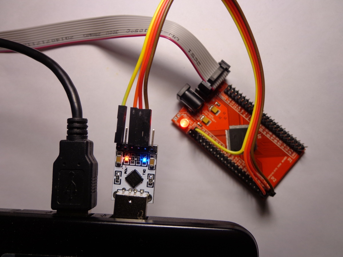
This module was tested on a motherboard with an Altera Max II EPM240T100C5N chip and a quartz resonator with a frequency of 50 megahertz, with a UART speed of 921600 baud (the maximum speed that my USB-UART adapter supports).
According to the standard, for the receiver, the sampling frequency of the start bit should be at least 16 times the UART frequency. So for the stable operation of the module at 921600 baud rate, the frequency of the quartz resonator should not be lower than 921600 * 16 = 14'745'600 Hz. For example, the crystal will go to 16 megahertz.
It is also desirable to put a pull-up resistor at the receiver input.
As usual, any optimization tips and improvements are welcome.
Download the updated files here .
Source: https://habr.com/ru/post/278005/
All Articles