Add instructions to the microprocessor MIPS, which work in the pipeline as his own
Is it possible to add instructions (commands) to the microprocessor? If you use FPGA / FPGA chips with reconfigurable logic and a microprocessor core, which are synthesized from the description in Verilog and VHDL languages, you can. Moreover, it will be an “honest”, true expansion of the instruction set, and not a trick of the type of software emulation of instructions in the exception handler from the reserved instruction, and not the “microcode” popular in the historical processors of the 1970s.
Commands added to a modern synthesized processor by modifying its source code on Verilog or VHDL can work in the pipeline and be processed by the processor as its own, without time delays.
The main problem with modifying the source design of the processor on Verilog or VHDL is the complexity. You need to understand how the logic of the various blocks works and avoid unwanted side effects. Fortunately, there is a processor expansion method that turns a semester student project into something that a student can design in one lab. This method is the CorExtend / UDI (User Defined Instructions) interface in the microprocessor core MIPS microAptiv UP, which is used in the package to form the MIPSfpga.
')
As part of Imagination Technologies' MIPSfpga university program, you can download this industrial code on the Verilog MIPS microAptiv UP processor.
https://community.imgtec.com/university/resources/
One of the common uses for UDI is bit manipulation in encryption algorithms. Another example is the creation of special instructions for accelerating DSP Accelerating DSP Filter Loops with MIPS® CorExtend® Instructions algorithms .
However, in the MIPSfpga documentation set, the interface between the kernel and CorExtend is not described in sufficient detail. Detailed documentation is provided only to licensees of kernels. This article presents my description of this interface based on the study of the source code. It can also be downloaded in pdf format. MIPS microAptiv UP Processor CorExtend UDI interface protocol guide .
CorExtend occupies the next place in the RTL hierarchy of the m14k microAptiv core.

All m14k_cpu level signals, including CorExtend UDI, are described in the MIPS32 microAptiv UP Processor Core Family Integrators Guide document (Table 2.3 Signal Descriptions for m14k cpu Level). It is better to look there, but for clarity, below is an excerpt from there exclusively with CorExtend UDI signals.
In addition to these signals, the CorExtend block has external signals with the number of bits determined by the developer.
To create your CorExtend block you need to change the files m14k_edp_buf misc and m14k_udi_stub should. In file
m14k_edp_buf_misc input and output ports can be connected, for example, like this.
The CorExtend block itself should replace the m14k_udi_stub file. An example of the interaction between CorExtend and the microAptiv UP kernel is presented in the timeline below.

The UDI_present signal must be pulled to one. UDI_honor_cee may be pulled to zero. If you pull it up to one, you will need to reset the Status CEE bit with the mtc0 instruction before executing CorExtend instructions. If this is not done, a CorExtend unusable exception will appear, and the next clock after UDI_start_e will set the UDI_kill_m signal to two clock cycles.
Partially, the instruction must be decoded on the same clock cycle at which the UDI_start_e signal appeared. This is necessary for generating a UDI_ri_e signal, which should be set at the same time as UDI_start_e appears if the instruction is reserved. If the instruction implies writing the result to the general register, its address must also be set to UDI_wrreg_e [4: 0] simultaneously with UDI_start_e. The remaining instruction fields can be written to the register and decoded later.
The signal UDI_wrreg_e [4: 0] can address 31 general-purpose registers, a value of 5'd0 means no entry to registers.
The result of the UDI instruction to be written to the general register must be set to UDI_rd_m [31: 0] on the next clock after UDI_start_e. If it is to be recorded later, on the next clock after UDI_start_e, you should set UDI_stall_m. UDI_stall_m should be reset to zero in one cycle before setting the result to UDI_rd_m [31: 0].
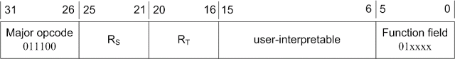
The figure below shows the general format of the UDI instruction. The Major opcode field is included in the special2 subset and is 6'd28. The RS and RT fields contain the addresses of the operand registers. Bits 15..6 can be used at the discretion of the developer. For example, there you can write the address of the destination register to record the result or send an instantaneous value. The Function field consists of bits 5..4, which are always 2'b01, and bits 3..0, with which you can encode up to 16 UDI instructions.
The development of the CorExtend block is illustrated by the following example of a DSP accelerator, which calculates the instantaneous power of a complex signal, which is defined as
P (t) = a 2 (t) + b 2 (t),
where a (t) and b (t) are the real and imaginary parts of the signal, respectively.
This operation is useful for detecting a signal by comparing it with a threshold value.
The table below lists the instructions for the DSP accelerator.
UDI0 calculates the instantaneous signal strength. The RS and RT operands contain 16-bit real and imaginary parts of the signal. The 32-bit result is written to the general register at address RD.
UDI1 does the same as UDI0. The difference is that UDI1 shifts the result to prevent overflow.
UDI2 calculates the instantaneous signal power using only the real part of the signal. RT operand is not used.
UDI3 writes a 32-bit threshold value to the internal register of the CorExtend block, the result is not returned.
UDI4, UDI5 and UDI6 perform the operations of the instructions UDI0, UDI1 and UDI2, respectively, and compare the result with a stored threshold value. If the threshold is exceeded, the result is 32'd1, otherwise 32'd0.
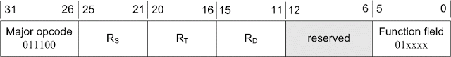
All instructions, except UDI3, write the results in general registers, for which it is necessary to specify its address. To do this, the RD field was entered, as shown in the figure below.
The code below shows an example program in MIPS assembly language for testing all the developed UDI instructions.
A sample project with the implementation of a CorExtend block with the above instructions can be downloaded at https://github.com/zatslogic/UDI_example .
The project includes the source code for the simulation, with the exception of files from the rtl_up directory. To get them, you must register with the Imagination University Program and request a download ( https://community.imgtec.com/downloads/mipsfpga-getting-started-version-1-2 ). Also, to run the simulation, you must have XilinxCorelib, you can compile it in Vivado using the compile_simlib command.
The project includes two options for the implementation of the CorExtend block. In the first case, all UDI instructions are executed in one cycle. In the second, additional registers were inserted and some instructions require more clocks to execute. This was done specifically to enable the UDI_stall_m signal.
On the time diagrams, the simulation of the above program in assembler is presented below.
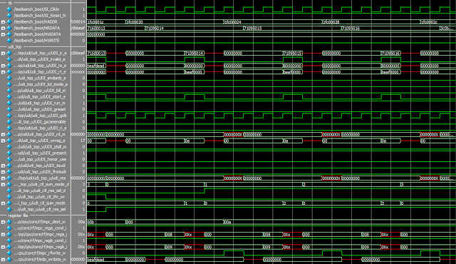
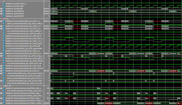
For the first one-stroke variant of the block, the instructions UDI0, UDI1 and UDI2 are executed as follows.

You can see the instructions appear on UDI_ir_e with the signals UDI_irvalid_e and UDI_start_e. Operands are also available on this clock. At the same tact, the address of the result record in the general register is formed. The result is set to UDI_rd_m on the next clock cycle.
In addition, the time diagram shows the signals of the block of general-purpose registers. The address of the entry in them can be seen on mpc_dest_w. The data is presented on edp_wrdata_w with the write enable signal to mpc_rfwrite_w. The signals mpc_rega_i and mpc_regb_i contain the addresses of operands read from general registers.
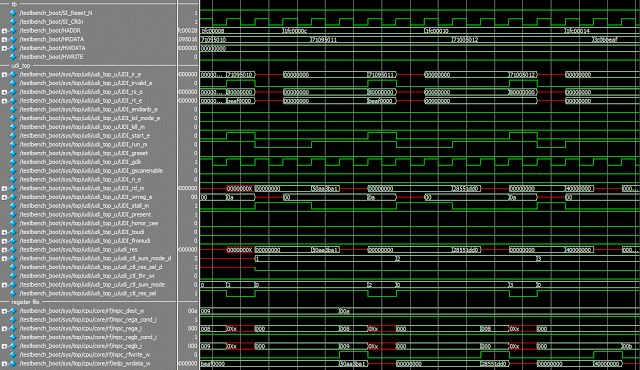
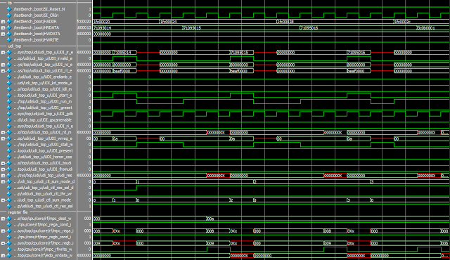
This timing diagram shows the execution of instructions UDI3, UDI4, UDI5 and UDI6.
As can be seen from the program's listing in assembler, UDI3 writes 0xbeafdead to the stored_threshold. The results of the execution of instructions UDI4, UDI5 and UDI6 are zero, because the threshold has never been exceeded.
In the following timing diagram, the instructions UDI3, UDI4, UDI5 and UDI6 are executed after the conditional transition. Now the threshold value is less than the results of calculations and you can see that 0x000001 is written to the result registers.

The following three timing diagrams show a UDI block simulation with additional registers.
This timing diagram shows the execution of instructions UDI0, UDI1 and UDI2. The signal UDI_stall_m is set for the duration of the calculations. On the next clock after its removal, the result is set to UDI_rd_m. Even after the beat, the result is recorded in general registers.
This timing diagram shows UDI4, UDI5 and UDI6 instructions with a UDI_stall_m signal.
On the diagram after it, the instructions UDI4, UDI5 and UDI6 are executed temporarily after the conditional transition.
I hope this material will be useful for those who want to also participate in the MIPSfpga program and create a project using UDI instructions.
Commands added to a modern synthesized processor by modifying its source code on Verilog or VHDL can work in the pipeline and be processed by the processor as its own, without time delays.
The main problem with modifying the source design of the processor on Verilog or VHDL is the complexity. You need to understand how the logic of the various blocks works and avoid unwanted side effects. Fortunately, there is a processor expansion method that turns a semester student project into something that a student can design in one lab. This method is the CorExtend / UDI (User Defined Instructions) interface in the microprocessor core MIPS microAptiv UP, which is used in the package to form the MIPSfpga.
')
As part of Imagination Technologies' MIPSfpga university program, you can download this industrial code on the Verilog MIPS microAptiv UP processor.
https://community.imgtec.com/university/resources/
One of the common uses for UDI is bit manipulation in encryption algorithms. Another example is the creation of special instructions for accelerating DSP Accelerating DSP Filter Loops with MIPS® CorExtend® Instructions algorithms .
However, in the MIPSfpga documentation set, the interface between the kernel and CorExtend is not described in sufficient detail. Detailed documentation is provided only to licensees of kernels. This article presents my description of this interface based on the study of the source code. It can also be downloaded in pdf format. MIPS microAptiv UP Processor CorExtend UDI interface protocol guide .
CorExtend occupies the next place in the RTL hierarchy of the m14k microAptiv core.
All m14k_cpu level signals, including CorExtend UDI, are described in the MIPS32 microAptiv UP Processor Core Family Integrators Guide document (Table 2.3 Signal Descriptions for m14k cpu Level). It is better to look there, but for clarity, below is an excerpt from there exclusively with CorExtend UDI signals.
| Signal name | Type of | Description |
| UDI_ir_e [31: 0] | Out | Full word instructions. Although the module receives rs and rt operands, the entire instruction is transmitted in order to be able to transmit data in the address fields of the operands. Note that the person who will implement his own UDI block must decode the Opcode and Function field on his own. |
| UDI_irvalid_e | Out | The valid signal for the instruction word (UDI_ir_e). |
| UDI_rs_e [31: 0] | Out | Operand rs. |
| UDI_rt_e [31: 0] | Out | Operand rt. |
| UDI_endianb_e | Out | Signals that the instruction is executed in Big Endian mode. The signal is usually not needed, unless a) the UDI instruction operates on part of the data word and is dependent on endian, b) the UDI block operates in big-endian mode. |
| UDI_kd_mode e | Out | Signals that the instruction is executed in kernel or debug mode. It can be used to prevent execution of certain instructions in kernel or debug modes. |
| UDI_kill_m | Out | The kill signal from the exception generated by the previous instruction. It can be used to remove UDI_stall_m, which will reduce the delay for multi-stroke UDI instructions whose results will not be used. |
| UDI_start_e | Out | The signal mpc_run_ie from the control unit (Master Pipeline Control). |
| UDI_run_m | Out | The signal mpc_run_m, used as valid for UDI_kill_m. |
| UDI_greset | Out | Reset, can be used to reset automata in a UDI block. |
| UDI_gclk | Out | Clock input in UDI block. |
| UDI gscanenable | Out | Global scan enable. |
| UDI_ri_e | In | Signals the Master Pipeline Control (MPC) that the currently executing instruction is reserved. However, the MPC will take it into account only if the instruction is included in a subset of the user-defined instructions of SPECIAL2 (bits [5: 4] in instruction 2'b01). |
| UDI_rd_m [31: 0] | In | 32-bit result of the executed instruction, available at the stage of M (Memory fetch). |
| UDI_wrreg_e [4: 0] | In | Register address for recording the result of a user-defined instruction. Also transmitted to MPC. |
| UDI_stall_m | In | Signals that the UDI block performs a multi-cycle instruction and must stop the pipeline before writing to the general register. must be set to 0 for one-cycle instructions. Signal stage M. |
| UDI_present | In | A static signal indicating that a UDI block is available. |
| UDI_honor_cee | In | Indicates whether the processor should take into account the CorExtend Enable (CEE) Status register bit. If the UDI_honor_cee is set to one and the Status.CEE bit of the Status register is not set, a CorExtend Unusable Exception exception is thrown. |
In addition to these signals, the CorExtend block has external signals with the number of bits determined by the developer.
| Signal name | Type of | Description |
| UDI_toudi [x-1: 0] | In | External input CorExtend block of variable length. |
| UDI_fromudi [x-1: 0] | Out | External output CorExtend block of variable length. |
To create your CorExtend block you need to change the files m14k_edp_buf misc and m14k_udi_stub should. In file
m14k_edp_buf_misc input and output ports can be connected, for example, like this.
assign UDI_ir_e[31:0] = mpc_ir_e ; assign UDI_irvalid_e = mpc_irval_e ; assign UDI_rs_e[31:0] = edp_abus_e ; assign UDI_rt_e[31:0] = edp_bbus_e ; assign UDI_endianb_e = cpz_rbigend_e ; assign UDI_kd_mode_e = cpz_kuc_e ; assign UDI_kill_m = mpc_killmd_m ; assign UDI_start_e = mpc_run_ie ; assign UDI_run_m = mpc_run_m ; assign UDI_greset = greset ; assign UDI_gscanenable = gscanenable ; assign UDI_gclk = gclk ; assign edp_udi_wrreg_e[4:0] = UDI_wrreg_e ; assign edp_udi_ri_e = UDI_ri_e ; assign edp_udi_stall_m = UDI_stall_m ; assign edp_udi_present = UDI_present ; assign edp_udi_honor_cee = UDI_honor_cee ; mvp_mux2 #(32) _res_m_31_0_(res_m[31:0],mpc_udislt_sel_m, asp_m, UDI_rd_m); The CorExtend block itself should replace the m14k_udi_stub file. An example of the interaction between CorExtend and the microAptiv UP kernel is presented in the timeline below.
The UDI_present signal must be pulled to one. UDI_honor_cee may be pulled to zero. If you pull it up to one, you will need to reset the Status CEE bit with the mtc0 instruction before executing CorExtend instructions. If this is not done, a CorExtend unusable exception will appear, and the next clock after UDI_start_e will set the UDI_kill_m signal to two clock cycles.
Partially, the instruction must be decoded on the same clock cycle at which the UDI_start_e signal appeared. This is necessary for generating a UDI_ri_e signal, which should be set at the same time as UDI_start_e appears if the instruction is reserved. If the instruction implies writing the result to the general register, its address must also be set to UDI_wrreg_e [4: 0] simultaneously with UDI_start_e. The remaining instruction fields can be written to the register and decoded later.
The signal UDI_wrreg_e [4: 0] can address 31 general-purpose registers, a value of 5'd0 means no entry to registers.
The result of the UDI instruction to be written to the general register must be set to UDI_rd_m [31: 0] on the next clock after UDI_start_e. If it is to be recorded later, on the next clock after UDI_start_e, you should set UDI_stall_m. UDI_stall_m should be reset to zero in one cycle before setting the result to UDI_rd_m [31: 0].
The figure below shows the general format of the UDI instruction. The Major opcode field is included in the special2 subset and is 6'd28. The RS and RT fields contain the addresses of the operand registers. Bits 15..6 can be used at the discretion of the developer. For example, there you can write the address of the destination register to record the result or send an instantaneous value. The Function field consists of bits 5..4, which are always 2'b01, and bits 3..0, with which you can encode up to 16 UDI instructions.
The development of the CorExtend block is illustrated by the following example of a DSP accelerator, which calculates the instantaneous power of a complex signal, which is defined as
P (t) = a 2 (t) + b 2 (t),
where a (t) and b (t) are the real and imaginary parts of the signal, respectively.
This operation is useful for detecting a signal by comparing it with a threshold value.
The table below lists the instructions for the DSP accelerator.
| Instruction | Description | function field |
| UDI0 R D ; R S ; R t | R D = R S [31:16] 2 + R T [31:16] 2 | 6'b010000 |
| UDI1 R D ; R S ; R t | R D = (R S [31:16] 2 + R T [31:16] 2 ) >> 1 | 6'b010001 |
| UDI2 R D ; R s | R D = R S [31:16] 2 | 6'b010010 |
| UDI3 R S | stored_threshold = R S | 6'b010011 |
| UDI4 R D ; R S ; R t | R D = ((R S [31:16] 2 + R T [31:16] 2 )> stored_threshold)? 1: 0 | 6'b010100 |
| UDI5 R D ; R S ; R t | R D = (((R S [31:16] 2 + R T [31:16] 2 ) >> 1)> stored_threshold)? 1: 0 | 6'b010101 |
| UDI6 R D ; R S ; R t | R D = (R S [31:16] 2 > stored_threshold)? 1: 0 | 6'b010110 |
UDI0 calculates the instantaneous signal strength. The RS and RT operands contain 16-bit real and imaginary parts of the signal. The 32-bit result is written to the general register at address RD.
UDI1 does the same as UDI0. The difference is that UDI1 shifts the result to prevent overflow.
UDI2 calculates the instantaneous signal power using only the real part of the signal. RT operand is not used.
UDI3 writes a 32-bit threshold value to the internal register of the CorExtend block, the result is not returned.
UDI4, UDI5 and UDI6 perform the operations of the instructions UDI0, UDI1 and UDI2, respectively, and compare the result with a stored threshold value. If the threshold is exceeded, the result is 32'd1, otherwise 32'd0.
All instructions, except UDI3, write the results in general registers, for which it is necessary to specify its address. To do this, the RD field was entered, as shown in the figure below.
The code below shows an example program in MIPS assembly language for testing all the developed UDI instructions.
Machine Code Instruction Address Assembly Code 3c088000 // bfc00000: lui $8, 0x8000 3c09beaf // bfc00004: lui $9, 0xbeaf 71095010 // bfc00008: udi0 $8 $9 $10 71095011 // bfc0000c: udi1 $8 $9 $10 71005012 // bfc00010: udi2 $8 $10 3c0bbeaf // bfc00014: lui $11, 0xbeaf 356bdead // bfc00018: ori $11,$11, 0xdead 71600013 // bfc0001c: udi3 $11 71095014 // bfc00020: L1: udi4 $8 $9 $10 71095015 // bfc00024: udi5 $8 $9 $10 71095016 // bfc00028: udi6 $8 $9 $10 3c0b0001 // bfc0002c: lui $11, 0x0001 356bfeed // bfc00030: ori $11,$11, 0xfeed 71600013 // bfc00034: udi3 $11 1000fff9 // bfc00038: beq $0, $0, L1 00000000 // bfc0003c: nop A sample project with the implementation of a CorExtend block with the above instructions can be downloaded at https://github.com/zatslogic/UDI_example .
The project includes the source code for the simulation, with the exception of files from the rtl_up directory. To get them, you must register with the Imagination University Program and request a download ( https://community.imgtec.com/downloads/mipsfpga-getting-started-version-1-2 ). Also, to run the simulation, you must have XilinxCorelib, you can compile it in Vivado using the compile_simlib command.
The project includes two options for the implementation of the CorExtend block. In the first case, all UDI instructions are executed in one cycle. In the second, additional registers were inserted and some instructions require more clocks to execute. This was done specifically to enable the UDI_stall_m signal.
On the time diagrams, the simulation of the above program in assembler is presented below.
For the first one-stroke variant of the block, the instructions UDI0, UDI1 and UDI2 are executed as follows.
You can see the instructions appear on UDI_ir_e with the signals UDI_irvalid_e and UDI_start_e. Operands are also available on this clock. At the same tact, the address of the result record in the general register is formed. The result is set to UDI_rd_m on the next clock cycle.
In addition, the time diagram shows the signals of the block of general-purpose registers. The address of the entry in them can be seen on mpc_dest_w. The data is presented on edp_wrdata_w with the write enable signal to mpc_rfwrite_w. The signals mpc_rega_i and mpc_regb_i contain the addresses of operands read from general registers.
This timing diagram shows the execution of instructions UDI3, UDI4, UDI5 and UDI6.
As can be seen from the program's listing in assembler, UDI3 writes 0xbeafdead to the stored_threshold. The results of the execution of instructions UDI4, UDI5 and UDI6 are zero, because the threshold has never been exceeded.
In the following timing diagram, the instructions UDI3, UDI4, UDI5 and UDI6 are executed after the conditional transition. Now the threshold value is less than the results of calculations and you can see that 0x000001 is written to the result registers.
The following three timing diagrams show a UDI block simulation with additional registers.
This timing diagram shows the execution of instructions UDI0, UDI1 and UDI2. The signal UDI_stall_m is set for the duration of the calculations. On the next clock after its removal, the result is set to UDI_rd_m. Even after the beat, the result is recorded in general registers.
This timing diagram shows UDI4, UDI5 and UDI6 instructions with a UDI_stall_m signal.
On the diagram after it, the instructions UDI4, UDI5 and UDI6 are executed temporarily after the conditional transition.
I hope this material will be useful for those who want to also participate in the MIPSfpga program and create a project using UDI instructions.
Source: https://habr.com/ru/post/276205/
All Articles