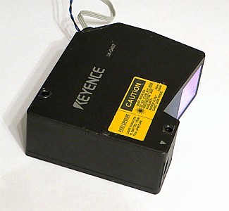
Reverse engineering laser distance sensor
One day, the Keyence LK-G407 non-operational laser distance sensor came to me. Not only was it non-working, it also could not be used without a special control unit. But the sensor has such interesting characteristics: distance measurement with an accuracy of micron units, and a work speed of 50 kilo-measurements / s. So, in order to run it, you will have to notice a lot in the sensor itself, and at the same time get valuable experience.
What is inside the sensor?
The optical part of the sensor is shown in the photo below:
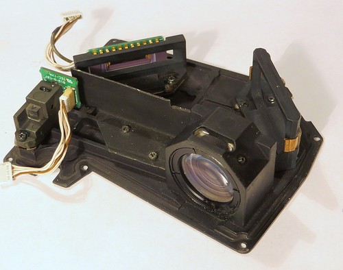
On the left in the photo is the laser module, behind it is a photosensitive ruler, on the right is a lens and a mirror.
From the design it becomes clear that this sensor can be attributed to the class of laser range finders with a triangulation method of measuring distance. The principle of operation of such rangefinders is well described here . In principle, it is quite simple - when the distance to the object to which the laser shines changes, the angle between the rangefinder lens and the laser spot changes. If in the focal plane of the lens to install a photosensitive ruler or matrix, then you can determine this angle by the position of the maximum output signal. Knowing the angle and distance between the laser and the lens, you can determine the distance to the object.
The advantages of this method are very high accuracy at small distances - under certain conditions it can be better than 0.1 microns!
It is also not a problem to measure the distance at high speed - you only need to use a high-speed photosensitive ruler.
The circuitry of such a rangefinder is also quite simple - due to the fact that there are no high frequencies in the device, and the primary signal amplification goes in the ruler itself.
But there is a drawback - the accuracy of the method drops sharply with increasing distance.
This sensor uses a long-focus lens (focal length of about 150 mm), therefore, to reduce the size of the sensor it includes a mirror.
And now it is worth going to the sensor electronics.
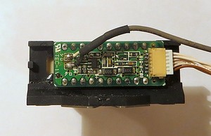
Here is the second part of the sensor:
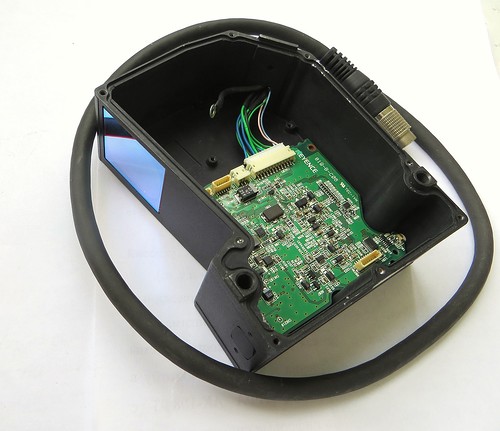
And the board itself:

And on the other hand:

The printed circuit board seems to be four-layered - most of the signal conductors are on the outer layers, the power lines are on the inner ones.
As I already mentioned, there was no control unit to the sensor, and without it it did not start working. It is clear that there were no circuits on the sensor either, the pinout of the cable and the sensor supply voltage were not even known. Conclusion - you need to do reverse-engineering schemes.
The result is such a scheme:
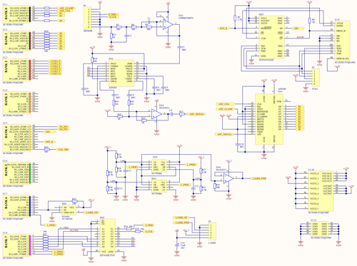
Of course, I did not begin to draw the entire sensor circuit, and figured out only the part related to FPGA. The numbers of the elements in the diagram do not correspond to the numbers on the board.
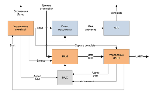
Thus, the block diagram of the sensor:

From it it is clear that the work of the entire sensor is controlled by two chips - FPGA Xilinx Spartan-3A and some custom chip. However, I was very lucky - from the diagram it is clear that the custom chip is connected only with FPGA. Thus, the FPGA itself is able to control all the signals in the sensor.
The key element of the whole structure is the photosensitive ruler. This line - obviously custom. Under the microscope on one of its edges is visible the inscription:
25-512
LI004-02
I assumed that 512 is the number of pixels in the ruler, and 25 is the width of the pixel in microns. As it turned out, I was right.
Behind the line is soldered a small board:
It contains an operational amplifier that increases the signal from the line 2 times and several resistors and capacitors. This board connects to P1. As can be seen from the diagram, only 3 signal lines go to the line. One of them is clearly an analog signal from its output (it is transmitted over a separate coaxial wire). The remaining two lines are digital, and are used to control the ruler. When analyzing the circuit, I was lucky again - when voltage is applied to the circuit on one of these lines (4), a frequency of 10 MHz appears. It immediately became clear that this line is responsible for the clocking of the ruler. Obviously, all ruler control is on the remaining line (3). I connected the line to the STM32F4 microcontroller, and started to send different signals to the (3) and (4) lines. As it turned out, the ruler works quite simply - as long as there is a high level on the line (3), there is an exposure - the ruler receives light. After installing the low level on the line (3), you need to apply 14 clock pulses to the ruler, after which it will output an analog signal to the next 512 clock pulses. The line operates on 5V voltage, and the FPGA - from 3.3V, and therefore the DD2 chip is used for level matching.
')
The analog signal from the ruler is transmitted via the low-pass filter to the repeater assembled on the DA1 chip. The signal is then fed to a P83-amplifier with a programmable gain AD8369 . The maximum gain of this microcircuit is 40 dB, and it can be adjusted programmatically by setting the necessary code at its inputs BIT0-3. This chip is designed to amplify the differential signal, and its output is also differential, so that then both of its outputs are connected to an operational amplifier DA4, amplifying the signal 2 times, and forming a single signal.
Next, the analog signal is fed to the input of a 10-bit AD9200 ADC. This chip was already familiar to me from the SDR receiver . In this case, it is connected in such a way that the voltage range digitized by it is (0.5-2.5) V. The digitized signal from the ADC output is transmitted to the FPGA.
It is worth paying attention to the CLAMP input of this ADC. This input is also controlled by FPGA. It is designed to bring the constant component of the input signal to a certain level.
Here is the scheme of the input stage of the ADC from the datasheet:

When a high level is applied to the CLAMP input, a voltage equal to the “CLAMP IN” input voltage appears at the amplifier output and at the AIN.
In this case, the capacitor CIN will be charged until the voltage on it becomes equal (Uin - Uclamp_in). After that, the input CLAMP set a low level, and the amplifier ceases to influence the operation of the ADC. In this sensor, the input "CLAMP IN" is connected to the lower reference voltage of the ADC + 0.5V. Thus, if there is some constant component at the output of DA4, then by using the CLAMP function, you can eliminate its influence on the result of the ADC operation.
After the first test configurations for the FPGA were written, it turned out that you really need to control the CLAMP signal, otherwise the signal from the ADC has a very large DC component. In my implementation, I simply applied 1 to it at that time, until the data is captured using the ADC.
From the diagram it can be seen that it uses a large number of supply voltages. I did not begin to draw diagrams of various power sources included in the sensor and various smoothing capacitors. As it turned out, the power pins (they are connected to a separate 2-pin connector) are connected to the TPS62050 DC-DC converter. The maximum voltage for it is 10V, the electronics have not yet started up from 6V, so I decided that the operating voltage of the sensor is 8V.
The laser diode used in this module is controlled by electronics mounted on a separate shawl:

I did not draw the circuit of this board. It connects to the main board via the P3 connector. As you can see, the control of the laser goes on two lines. One of them (3) is connected to the FPGA via an inverter, and is responsible for turning on the laser — it is turned on at a low level at the FPGA output. Another line (4) is needed to control the laser power. This is an analog line, and in order to change the voltage on it, the DAC, assembled on DA5-7 microcircuits, is included in the circuit (I did not understand why the developers built up such an intricate circuit, and did not take the finished DAC chip).
As it is known, most FPGAs do not contain non-volatile memory, respectively, the FPGA configuration should be stored in an external chip. In this case, this is the DD3 XCF01 - a specialized flash memory chip. When enabled, the FPGA automatically reads the configuration from it into its memory. The FPGA and XCF01 are connected to the JTAG circuit, which is connected to the P2 connector. As a result, you can program the XCF01 in-situ via this connector, configure the FPGA and debug it.
So I figured out how the sensor electronics work, and I got a part of its circuit. Now you can start the experiments, i.e. FPGA programming. It is worth noting that before that I had not dealt with the FPGA manufactured by Xilinx. I also didn’t have the necessary programmer, so I had to make it myself by combining several OpenSource projects.
The programmer worked fine, and I managed to launch simple projects on the FPGA — simple switching of the FPGA outputs. However, in the future I needed a connection with a computer. I didn’t want to communicate with the LVDS interface (at the port where the LVDS power supply line is 2.5V), so I just cut the two tracks connecting the FPGA and ASIC. There was a connector on the board, apparently intended for setting up or testing ASIC, I could not use it, so I also cut two tracks going to it, and connected the connector pins to the FPGA. Now you can connect a USB-UART adapter to this connector.
Type of board after revision:

After that, I wrote a simple program to test the operation of the UART. It worked - the computer correctly received single bytes transmitted over the UART with the FPGA. The next step is to transfer data from the photosensitive line to the computer. I used this block diagram of the FPGA program:
View of the scheme in ISE:
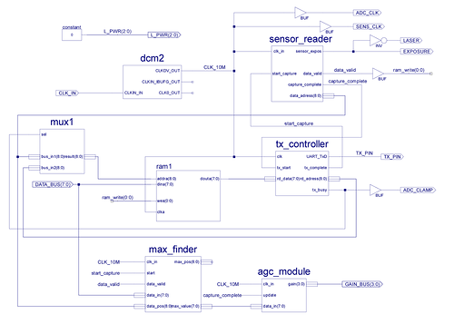
The top-level project is drawn in the schematic editor, and all modules included in it are written in Veriolg. The principle of the project is quite simple - the data from the ruler, digitized by the ADC, are captured by the FPGA and stored in the RAM. After all 512 elements of the signal are captured, they are transmitted via the UART to the computer. After all the data has been transmitted, the cycle repeats. The sensor_reader module in this project controls the ruler, the laser, and the CLAMP signal. The control is implemented in the simplest way - a clock counter controls all signals. The tx_controller module includes a UART transmitter module. It is designed to transfer data that the module receives from external memory.
During operation, the level of the useful signal on the ruler can vary greatly - due to a change in the distance to the object and a change in its reflectance. If the signal is too small, measurements become impossible, and if the signal is too large, the measurement accuracy drops dramatically. Because of this, the gain of the analog signal needs to be adjusted. Initially, the project included a UART receiver module that allowed you to manually change the gain, later I removed it and made an automatic gain control - AGC.
It includes the maximum signal search module (“max_finder”) and the AGC module itself (“agc_module”). This module is also quite simple - if the signal level is less than 170, then the gain increases, if more than 250, it decreases.
All modules, line and ADC are clocked from 10 MHz frequency. I made the exposure time equal to 5 µs. Thus, the entire process of exposure and signal capture in the FPGA takes (5 + 51) μs. Data transmission time is much longer - at a clock frequency of 500,000 bps, transmission of 512 bytes takes 10 ms, which gives 100 measurements per second.
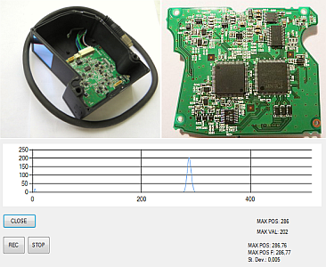
To view the transmitted data in real time, a simple C # program was written:

When moving an object along a laser beam, the position of the peak peak changes. A simple calculation of the position of the maximum gives a low measurement accuracy, since the ruler contains only 512 pixels. Therefore, to more accurately measure the position of the maximum of the signal, it is necessary to use center of gravity search algorithms, which make it possible to determine the coordinates of the maximum of the signal with sub-pixel accuracy.
I used this formula to find the peak center of gravity:
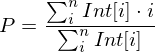
where n is the total number of pixels, Int [i] is the intensity i of a pixel.
In order for the various noise present in the signal to not degrade the accuracy of operation, it is useful to process only samples that exceed a certain threshold and are close to the peak maximum. This is especially important in the case when the gain is not enough, and the useful signal does not exceed half of the ADC scale. Moreover, with increasing gain, the noise level increases, which worsens the situation. In the above program, this is taken into account.
In the picture above, MAX POS is the value calculated by this formula, MAX POS F is the average value of the last 50 measurements.
As I have already said, the resulting measurement frequency is 100 Hz, and it is limited by the speed of data transmission over the UART. However, it is not necessary to process the signal on the computer, it can be done on the FPGA, due to which you can multiply the speed of measurements.
As a result, a program was developed for the FPGA with the following structural scheme:

View of the scheme in ISE:

As you can see, some of the modules are taken from the previous project.
In this case, the centroid_finder module is engaged in calculating the position of the center of gravity (centroid) of the signal. In order to limit the data analysis area, the coarse value of the position of the maximum and its amplitude are transferred to the module.
Since these values can be calculated only by analyzing the entire signal (that is, they appear with a delay of 512 clock pulses), it turns out that the digitized data must be fed to the input “centroid_finder” with the same delay. In order to hold the data for 512 clocks, the FIFO buffer is used. For the initial filling of the FIFO, the “fifo_logic” module is used - it prohibits reading from the FIFO if it is not filled.
The “tx_controller_3bytes” module sequentially transmits 3 bytes, the first of them is zero, the remaining two contain the calculated position of the center of gravity. At a speed of 50000 bit / s, the transmission of 3 bytes takes 60 µs - almost the same as the capture of a signal. Zero byte is used to synchronize data - after it always goes high byte.
Data transmission over the UART and data capture are triggered simultaneously by the start_capture signal. This signal is generated if the previous transmission is over at the same time and a new position of the center of gravity is calculated. As a result, the distance measurement and data transmission time is close to 60 μs, which gives the coordinate measurement speed - 16.6 KSPS. This is less than stated by the sensor manufacturer. It indicates the minimum measurement time - 20 µs (this corresponds to 50 KSPS), although it is not clear how this time is obtained, because even at the maximum speed of the AD9200 - 20 MSPS, the signal capture time from 512 pixels will be - 25.6 µs. And this is without taking into account the time of exposure.
As I said earlier, this sensor did not work. As far as I know, the problem was that it was installed on a highly vibrating industrial installation, and because of the vibration, the laser of the sensor failed (the sensor stopped responding to dark surfaces).
Unfortunately, there was no marking on the native diode. I tried to replace the laser diode in the laser module with a purchased 5 mW laser diode, but after a while its intensity dropped. Most likely, the electronics of the laser module was designed for a more powerful diode (although operating in a pulsed mode, due to which the average radiation level is quite low).
In order to at least somehow start the sensor, I made my laser diode driver working in the constant-radiation mode:

The native laser diode of the sensor was rolled into the metal case of the laser module, so the new laser diode just had to be glued to the module. At the same time, the overall dimensions of the diode used were somewhat different from the dimensions of the native diode, which is why I never managed to focus the laser module qualitatively.
This is the assembled sensor:
In order to use the sensor to measure the distance, it is necessary to calibrate it, i.e. determine the law relating the result returned by the sensor and the actual distance. The calibration process itself is a series of measurements, as a result of which a set of distances from the sensor to an object and the corresponding results are formed.
The distance between the sensor and the object must be measured very accurately. For calibration, I made a stand that includes a linear encoder and the laser sensor itself:

The distance is measured to the plate attached to the end of the encoder.
After all the data is collected, you can conduct a regression analysis in Mathcad.
As a result, I got this expression:
value_mm = 70.0 / Tan (-0.000277757 * max_pos + 0.28355) - 366.23554
Obviously, the values of the constants in terms of the position of the details of the sensor. The slightest shift in details will cause the calculated distance value to be incorrect. Therefore, all parts must be very firmly fixed.
The video below shows how you can process data from the sensor:
The first part of the video shows what the signal from the photosensitive ruler looks like. It is clearly seen that if the object is dark, the amplitude does not change (due to the operation of the AGC), but the noise level greatly increases.
In the second part of the video, the program takes from the sensor the position of the center of gravity, and recounts it into the distance. The value of the distance to the object received from the encoder is also transferred to the program. Under the distance of the encoder, the difference between these distances is displayed. It can be seen that when moving, the difference becomes greater than 1 mm (this is due to delays during transmission of distances and their display), but during the stops at any distance the difference does not exceed 0.03 mm.
In order to make the data from the sensor easier to analyze, I wrote a program that stores the data received from the sensor in wav format. Such files can be opened in sound editors, and various filters can be applied to them.
Here, for example, looks like a signal from a sensor that was directed to the wall of a transformer power supply:
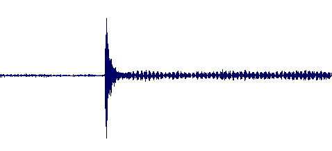
It can be seen as when turning on the power supply began to vibrate.
I tried to direct the sensor to the speaker cone on which the music is played - and after processing it was really audible in the audio editor.
Taim way, I managed to give a non-working sensor a new life (I may need it in future projects), and at the same time get experience with Xilinx FPGA.
Projects for FPGA
Source: https://habr.com/ru/post/274879/
All Articles