“Stupid” watches on FPGA
Hello to all!
I decided to write another article that would be useful for novice developers in the field of FPGA. He postponed the moment of publication for a very long time, the material itself was prepared several months ago, but somehow it didn’t get around to sit down and write all this in the whole article. But at last free time appeared, therefore I invite all interested in reading.

The project is called a “stupid clock” because it doesn’t know anything except how to count the time and date and display them. First of all, the project is designed for senior students and beginners. There are no unusual blocks in it, vendor IP cores are not used, and even more so there are no complicated exchange interfaces (such as PCIe, Ethernet, USB, etc.).
This time the project on programmable logic integrated circuits (FPGAs) will be primitive and extremely simple, and I will try to tell you about all the difficulties that I had to face in carrying out the task.
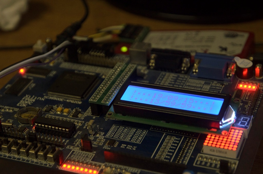
Debugging board: the same small and simple devkit based on Spartan3E FPGA. Its characteristics:
')
Key Features:
From this list, we will need directly the FPGA itself, which will manage this whole business. Two devices are also needed (DS1302 chip and LCD1602 display) and several trigger switches.
DS1302 - timer with serial interface transfer (manufactured by Maxim Integrated),
LCD1602 - LCD display with the ability to display two lines of 16 characters (manufactured by Noname).
Below is a block diagram of the connections:

Let us turn to the description of the used chips.
The DS1302 is a small microchip that uses three lines for data exchange, which form a serial interface.
The main feature of the chip is that the passage of time does not stop, even if the FPGA and the display is disconnected from the power supply. The timer allows you to count seconds, minutes, hours, days of the week, days, months, as well as years, that is, a full set of "hours."
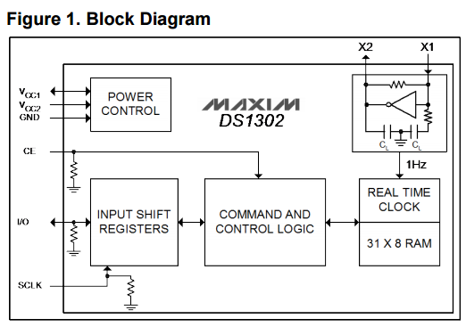
Also, the chip stores the latest "stitched" values of time and date. But by itself, the chip is "stupid", that is, it needs to set all the parameters, including the day of the week. Inside the timer there is a counter, which correctly increments the time and date values, if everything was properly flashed on the chip.
A quartz oscillator tuned to the frequency f = 32.768 kHz is connected to the chip from the outside.
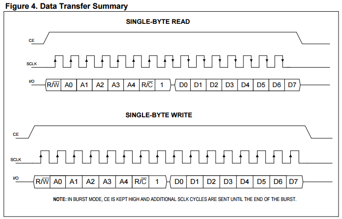
The following figure shows the interface for exchanging data in read and write mode:
How it works?
a) In order to record or read any value from the timer, it is necessary at the time of the transmission to set the high level (logical 1) to the CE input,
b) Depending on the read or write operation, with a high CE level, 15 or 16 clocks are required, respectively. The operation of writing data from the I / O input occurs on the rising edge of the SCLK clock signal, and the data reading operation occurs on the falling edge of the SCLK signal. The data is transmitted in order from the low-order bit to the high-order one.
c) The first byte in the transmission process is always overhead and is always “written” to the timer. This means that it selects the type and direction of the transmitted command. The zero bit of R / W is responsible for the type of operation: “read” - at high level, “write” - at low signal level. Bit field from 1 to 5 sets the address of the command or the internal memory of the timer. The sixth bit defines work with timer registers or internal memory: “memory” at high logic level, “timer” at low logic level. The seventh bit should always be set to 1 (if the seventh bit is randomly equal to 0, then the timer does not respond to the command).
d) Second byte - data written to or read from the timer.
The following figure shows a table of timer commands:

How to work with the table?
The table shows that the timer processes the data in binary coded decimal format (BCD) . In this regard, further on the FPGA you will have to write a data converter from binary format to binary-decimal.
Example: to read seconds from a timer, you need to create a command byte 0x81. To record the minutes, you need to create a command byte 0x82.
When working with a timer chip, there is a small subtlety, because of which I killed a whole day in search of problems and even rewrote the timer controller on the FPGA a couple of times. Therefore, I urge everyone to read the datasheets more attentively. :)
To record the date and time in the microcircuit, you must first "allow recording". See in the table at addresses 0x8F and 0x8E bit WP (write protect)? By default, the bit is at 0, which means a ban on any write operations. Therefore, to write the date and time to the microcircuit, you must first transfer WP to the state of logical one. This is done by sending two bytes one after another (command and data): 0x8E 0x80 . After that, the timer will become obedient and allow you to write information to yourself.
Also note the 7 bits in the seconds register - CH (clock halt). The timer stops if this bit is in high state. Therefore, when you first write to the register of seconds, you need to reset the most significant bit.
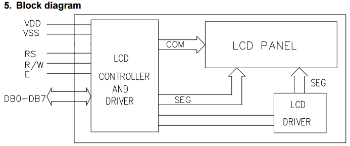
LCD1602 is a normal LCD display that allows you to display two lines of 16 characters each, using a parallel exchange interface. The interface is primitive and simple.
I used the display in recording mode, that is, the port R / W = 0 always. In connection, data exchange is somewhat simplified, as is the controller itself implemented on the FPGA.
How to work with the display?
Before each first display, it is necessary to initialize it with a set of commands that are given in the datasheet.
For my implementation of the display controller, this was a set of four commands that were executed sequentially one after another each time the firmware was started. Several initialization bytes must be sent to the DB line:
0x00 (or 0x01) - clears the display.
0x38 - sets the number of lines and font size (I need 2 lines of 16 characters each with the maximum size of characters).
0x0C - sets the cursor to the on / off position. ("Incl." In my case).
0x06 - sets the direction of the cursor movement and the shift on the display (to the right, ie the increment of the shift counter).
In this case, the signals RS and R / W must be in a state of logical zero.
After the initialization process, commands and data are transmitted through the DB line in turn. The command determines the position of the character on the display, the data determines the character from the table below.
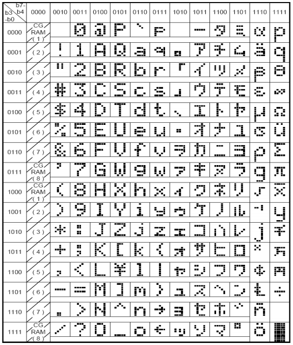
For example, to write the character " Q " you need to write the number 0x51 along the DB line. Thus, the entire transfer of data on the display is reduced to the choice of position and character.
Let us turn to the implementation of the project on the FPGA. The programming language used in the project is VHDL. Differs from the rest of its simplicity and at the same time cumbersome structures.
In order for the clock to start ticking, and the display to display the date and time you need to do several actions that, in principle, are made for each project on the FPGA. Required:
UCF
Let's start with the simple. Determine the pins that will be used in the project.
In the UCF file, the port name used in the top-level file, the pin to which it is connected, as well as other parameters (electrical type, current level, driver speed, pull-up, etc.) are specified. Signals for connecting to the timer and LCD display were described above, therefore I will give a description of the missing ports connected to the switches.
The second pitfall I encountered is that the devikit developers forgot to connect the timer chip to the FPGA. But, fortunately, they brought the serial interface to the pins, which I connected with other pins, connected by conductors, directly to the FPGA.
Hdl
Next is written timer controller and display controller. There is no point in presenting the full text on VHDL here, but I’ll tell you about the principles of data exchange. During the initial start-up (when all control signals are set and reset), the LCD display is initialized, and the date and time constants defined in the top-level file are written to the timer. Below is the code of the function to convert data from binary to binary decimal format:
The following figure shows the timing diagrams obtained during the debugging of the timer controller. Bold lines are allocated to the serial transfer interface. Three data_i, data_o, data_t lines are connected to the IOBUF I / O port in the top-level file.

Inside the FPGA in an infinite loop begins to poll the timer registers responsible for setting the time (0x80-0x8D). Registers are polled in a circle, starting with the years and ending with seconds. After each reading from the timer, the data is entered into the registers of the FPGA bearing the typical names (second, minute, etc.). After receiving the resolution signal from the LCD controller, the data from the timer controller is transmitted to the control node for the display controller. Depending on the type of the timer register and its value, the data is converted into the format required for the display and set the desired position on the display by setting the appropriate address. The LCD controller receives the data from the timer and writes it to a dual-port 8x32 RAM-memory in the FPGA, performed on the distributed logic of the crystal (cell SLICEM). Then the controller reads all the information from the memory and thereby updates the characters on the LCD display. The whole project operates at a relatively high frequency of 50 MHz, so it’s unrealistic to see any delays when counting seconds with an eye.
The following figure shows the placement of the project in the FPGA chip.

Green lines indicate connections of input / output ports to internal FPGA resources, the Blue area is the area of logic gates, the red rectangles are a bunch of built-in multipliers 18x18 and RAMB16K block memory, the orange squares are digital clocks manager DCM synthesis blocks. The rectangles are highlighted in purple - „p-block“, within the boundaries of which one or another component of the project is bred with the option “Keep Hierarchy” enabled. White highlighted areas are cells of controllers and test modules. The remaining p-blocks were left from my old project on the FPGA , I decided not to delete them (what if someone wants to play a sapper?).
So, in the course of the work, the FPGA firmware was created to connect the timer with the LCD display.
With the help of Aldec Active-HDL CAD, a temporary modeling of the project was carried out, as well as all the writing of code and models. In the Xilinx ISE Design Suite environment, the project was synthesized and traced on the FPGA Spartan3E. Also used aids: PlanAhead - used for pinout, the location of the project nodes in the crystal and tracing. ChipScope Pro - is used for debugging in real hardware by loading special debug kernels into FPGA.
Automatic project documentation
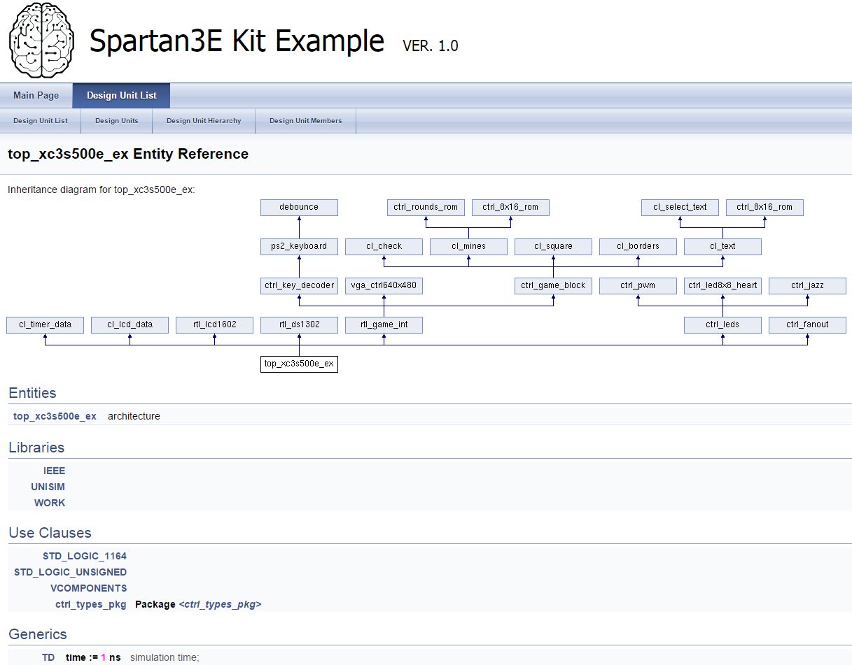
It so happened that during the creation of this project, we had at work proposed another attempt at introducing the source code documentation. One solution was to use the Doxygen automated documentation tool. I really like how hierarchy graphs are built in this application. For HDL projects this is a very important point. On Habré there are several articles on this tool . In conjunction with the HTML Help Workshop , Doxygen allows you to generate only one documentation file in CHM format.
Unfortunately, the attempt to implement failed, but the experience with the tool remained. Therefore, for the project of “stupid” clocks on FPGA, I decided to use automatic documentation. On the githaba in the project folder is the configuration file for DoxyWizard and the result of its work. Here is one page of what happened in the documentation process.
The source code on github is LCD Timer on FPGA .
Video demonstration of the project performance:
Do not be surprised by the date displayed on the display. The material was filmed and prepared a long time ago, and only now came to the article. Lazy to retake ... :)
Related projects:
I decided to write another article that would be useful for novice developers in the field of FPGA. He postponed the moment of publication for a very long time, the material itself was prepared several months ago, but somehow it didn’t get around to sit down and write all this in the whole article. But at last free time appeared, therefore I invite all interested in reading.
The project is called a “stupid clock” because it doesn’t know anything except how to count the time and date and display them. First of all, the project is designed for senior students and beginners. There are no unusual blocks in it, vendor IP cores are not used, and even more so there are no complicated exchange interfaces (such as PCIe, Ethernet, USB, etc.).
This time the project on programmable logic integrated circuits (FPGAs) will be primitive and extremely simple, and I will try to tell you about all the difficulties that I had to face in carrying out the task.
Initial data
Debugging board: the same small and simple devkit based on Spartan3E FPGA. Its characteristics:
')
Key Features:
- FPGA Spartan3E ( XC3S500E-4PQ208C ) - 500K logic gates,
- Clock source CLK = 50 MHz,
- 64M SDRAM external memory,
- SPI Flash (M25P80) for storing FPGA firmware,
- LED matrix 8x8, LED line 8 pcs.,
- 8 switches and 5 buttons,
- Connectors for connecting LED displays,
- VGA connector for connecting the display,
- DS1302 timer ,
- LCD1602 display
- PS / 2 connectors, etc.
From this list, we will need directly the FPGA itself, which will manage this whole business. Two devices are also needed (DS1302 chip and LCD1602 display) and several trigger switches.
DS1302 - timer with serial interface transfer (manufactured by Maxim Integrated),
LCD1602 - LCD display with the ability to display two lines of 16 characters (manufactured by Noname).
Below is a block diagram of the connections:
Let us turn to the description of the used chips.
Timer
The DS1302 is a small microchip that uses three lines for data exchange, which form a serial interface.
- CE - clock enable, enables SCLK clocking.
- SCLK - clock signal (maximum frequency of operation = 2 MHz).
- I / O is an input / output port through which data and commands are transmitted in serial form.
The main feature of the chip is that the passage of time does not stop, even if the FPGA and the display is disconnected from the power supply. The timer allows you to count seconds, minutes, hours, days of the week, days, months, as well as years, that is, a full set of "hours."
Also, the chip stores the latest "stitched" values of time and date. But by itself, the chip is "stupid", that is, it needs to set all the parameters, including the day of the week. Inside the timer there is a counter, which correctly increments the time and date values, if everything was properly flashed on the chip.
A quartz oscillator tuned to the frequency f = 32.768 kHz is connected to the chip from the outside.
The following figure shows the interface for exchanging data in read and write mode:
How it works?
a) In order to record or read any value from the timer, it is necessary at the time of the transmission to set the high level (logical 1) to the CE input,
b) Depending on the read or write operation, with a high CE level, 15 or 16 clocks are required, respectively. The operation of writing data from the I / O input occurs on the rising edge of the SCLK clock signal, and the data reading operation occurs on the falling edge of the SCLK signal. The data is transmitted in order from the low-order bit to the high-order one.
c) The first byte in the transmission process is always overhead and is always “written” to the timer. This means that it selects the type and direction of the transmitted command. The zero bit of R / W is responsible for the type of operation: “read” - at high level, “write” - at low signal level. Bit field from 1 to 5 sets the address of the command or the internal memory of the timer. The sixth bit defines work with timer registers or internal memory: “memory” at high logic level, “timer” at low logic level. The seventh bit should always be set to 1 (if the seventh bit is randomly equal to 0, then the timer does not respond to the command).
d) Second byte - data written to or read from the timer.
The following figure shows a table of timer commands:
How to work with the table?
The table shows that the timer processes the data in binary coded decimal format (BCD) . In this regard, further on the FPGA you will have to write a data converter from binary format to binary-decimal.
Example: to read seconds from a timer, you need to create a command byte 0x81. To record the minutes, you need to create a command byte 0x82.
When working with a timer chip, there is a small subtlety, because of which I killed a whole day in search of problems and even rewrote the timer controller on the FPGA a couple of times. Therefore, I urge everyone to read the datasheets more attentively. :)
To record the date and time in the microcircuit, you must first "allow recording". See in the table at addresses 0x8F and 0x8E bit WP (write protect)? By default, the bit is at 0, which means a ban on any write operations. Therefore, to write the date and time to the microcircuit, you must first transfer WP to the state of logical one. This is done by sending two bytes one after another (command and data): 0x8E 0x80 . After that, the timer will become obedient and allow you to write information to yourself.
Also note the 7 bits in the seconds register - CH (clock halt). The timer stops if this bit is in high state. Therefore, when you first write to the register of seconds, you need to reset the most significant bit.
LCD
LCD1602 is a normal LCD display that allows you to display two lines of 16 characters each, using a parallel exchange interface. The interface is primitive and simple.
- DB [7: 0] - parallel command / data bus.
- RS - register select, select signal: '0' - commands, '1' - data.
- R / W - data transfer direction ('0' - write / '1' - read).
- E - enable, synchronization, set to a logical unit at the moment of transmission through the DB line
I used the display in recording mode, that is, the port R / W = 0 always. In connection, data exchange is somewhat simplified, as is the controller itself implemented on the FPGA.
How to work with the display?
Before each first display, it is necessary to initialize it with a set of commands that are given in the datasheet.
For my implementation of the display controller, this was a set of four commands that were executed sequentially one after another each time the firmware was started. Several initialization bytes must be sent to the DB line:
0x00 (or 0x01) - clears the display.
0x38 - sets the number of lines and font size (I need 2 lines of 16 characters each with the maximum size of characters).
0x0C - sets the cursor to the on / off position. ("Incl." In my case).
0x06 - sets the direction of the cursor movement and the shift on the display (to the right, ie the increment of the shift counter).
In this case, the signals RS and R / W must be in a state of logical zero.
After the initialization process, commands and data are transmitted through the DB line in turn. The command determines the position of the character on the display, the data determines the character from the table below.
For example, to write the character " Q " you need to write the number 0x51 along the DB line. Thus, the entire transfer of data on the display is reduced to the choice of position and character.
FPGA Project
Let us turn to the implementation of the project on the FPGA. The programming language used in the project is VHDL. Differs from the rest of its simplicity and at the same time cumbersome structures.
In order for the clock to start ticking, and the display to display the date and time you need to do several actions that, in principle, are made for each project on the FPGA. Required:
- two independent controllers - for DS1302 and for LCD1602.
- two test bundles - to set the start time and to initialize the display.
- top level file linking it all together.
- FPGA pinout file (UCF file).
UCF
Let's start with the simple. Determine the pins that will be used in the project.
## CLK 50 MHz NET "CLK" LOC = "P183" | IOSTANDARD = LVCMOS33 ; ## Switches NET "RESET" LOC = "P148" | IOSTANDARD = LVTTL | PULLUP ; ## SW<0> NET "START" LOC = "P130" | IOSTANDARD = LVTTL | PULLUP ; ## SW<3> NET "RESTART" LOC = "P124" | IOSTANDARD = LVTTL | PULLUP ; ## SW<4> NET "TEST_LCD" LOC = "P118" | IOSTANDARD = LVTTL | PULLUP ; ## SW<5> ## LCD ports NET "LCD_RS" LOC = "P77" | IOSTANDARD = LVTTL | DRIVE = 8 | SLEW = FAST ; NET "LCD_RW" LOC = "P68" | IOSTANDARD = LVTTL | DRIVE = 8 | SLEW = FAST ; NET "LCD_EN" LOC = "P65" | IOSTANDARD = LVTTL | DRIVE = 8 | SLEW = FAST ; NET "LCD_DT<0>" LOC = "P49" | IOSTANDARD = LVTTL | DRIVE = 8 | SLEW = FAST ; NET "LCD_DT<1>" LOC = "P48" | IOSTANDARD = LVTTL | DRIVE = 8 | SLEW = FAST ; NET "LCD_DT<2>" LOC = "P40" | IOSTANDARD = LVTTL | DRIVE = 8 | SLEW = FAST ; NET "LCD_DT<3>" LOC = "P50" | IOSTANDARD = LVTTL | DRIVE = 8 | SLEW = FAST ; NET "LCD_DT<4>" LOC = "P62" | IOSTANDARD = LVTTL | DRIVE = 8 | SLEW = FAST ; NET "LCD_DT<5>" LOC = "P98" | IOSTANDARD = LVTTL | DRIVE = 8 | SLEW = FAST ; NET "LCD_DT<6>" LOC = "P64" | IOSTANDARD = LVTTL | DRIVE = 8 | SLEW = FAST ; NET "LCD_DT<7>" LOC = "P63" | IOSTANDARD = LVTTL | DRIVE = 8 | SLEW = FAST ; # SERIAL PORTS VIA HEADEX NET "T_CE" LOC = "P147" | IOSTANDARD = LVTTL | SLEW = SLOW | DRIVE = 8 ; NET "T_CK" LOC = "P146" | IOSTANDARD = LVTTL | SLEW = SLOW | DRIVE = 8 ; NET "T_DT" LOC = "P145" | IOSTANDARD = LVTTL | SLEW = SLOW | DRIVE = 8 ; In the UCF file, the port name used in the top-level file, the pin to which it is connected, as well as other parameters (electrical type, current level, driver speed, pull-up, etc.) are specified. Signals for connecting to the timer and LCD display were described above, therefore I will give a description of the missing ports connected to the switches.
- RESET - '0' - global reset FPGA.
- START - '1' - start for LCD display (starts initialization and data transfer process).
- RESTART - '0' - restart the timer (translates the date and time to the state defined in the FPGA memory).
- TEST_LCD - port for test purposes, '0' - displays data from the timer, '1' displays a static message (“hello habr ').
The second pitfall I encountered is that the devikit developers forgot to connect the timer chip to the FPGA. But, fortunately, they brought the serial interface to the pins, which I connected with other pins, connected by conductors, directly to the FPGA.
Hdl
Next is written timer controller and display controller. There is no point in presenting the full text on VHDL here, but I’ll tell you about the principles of data exchange. During the initial start-up (when all control signals are set and reset), the LCD display is initialized, and the date and time constants defined in the top-level file are written to the timer. Below is the code of the function to convert data from binary to binary decimal format:
---------------- INTEGER TO STD_LOGIC_VECTOR TO BCD CONVERTER ---------------- constant n : integer:=8; constant q : integer:=2; function to_bcd ( bin : std_logic_vector((n-1) downto 0) ) return std_logic_vector is variable i : integer:=0; variable j : integer:=1; variable bcd : std_logic_vector(((4*q)-1) downto 0) := (others => '0'); variable bint : std_logic_vector((n-1) downto 0) := bin; begin for i in 0 to n-1 loop -- repeating 8 times. bcd(((4*q)-1) downto 1) := bcd(((4*q)-2) downto 0); --shifting the bits. bcd(0) := bint(n-1); bint((n-1) downto 1) := bint((n-2) downto 0); bint(0) :='0'; l1: for j in 1 to q loop if(i < n-1 and bcd(((4*j)-1) downto ((4*j)-4)) > "0100") then --add 3 if BCD digit is greater than 4. bcd(((4*j)-1) downto ((4*j)-4)) := bcd(((4*j)-1) downto ((4*j)-4)) + "0011"; end if; end loop l1; end loop; return bcd; end to_bcd; The following figure shows the timing diagrams obtained during the debugging of the timer controller. Bold lines are allocated to the serial transfer interface. Three data_i, data_o, data_t lines are connected to the IOBUF I / O port in the top-level file.
Inside the FPGA in an infinite loop begins to poll the timer registers responsible for setting the time (0x80-0x8D). Registers are polled in a circle, starting with the years and ending with seconds. After each reading from the timer, the data is entered into the registers of the FPGA bearing the typical names (second, minute, etc.). After receiving the resolution signal from the LCD controller, the data from the timer controller is transmitted to the control node for the display controller. Depending on the type of the timer register and its value, the data is converted into the format required for the display and set the desired position on the display by setting the appropriate address. The LCD controller receives the data from the timer and writes it to a dual-port 8x32 RAM-memory in the FPGA, performed on the distributed logic of the crystal (cell SLICEM). Then the controller reads all the information from the memory and thereby updates the characters on the LCD display. The whole project operates at a relatively high frequency of 50 MHz, so it’s unrealistic to see any delays when counting seconds with an eye.
The following figure shows the placement of the project in the FPGA chip.
Green lines indicate connections of input / output ports to internal FPGA resources, the Blue area is the area of logic gates, the red rectangles are a bunch of built-in multipliers 18x18 and RAMB16K block memory, the orange squares are digital clocks manager DCM synthesis blocks. The rectangles are highlighted in purple - „p-block“, within the boundaries of which one or another component of the project is bred with the option “Keep Hierarchy” enabled. White highlighted areas are cells of controllers and test modules. The remaining p-blocks were left from my old project on the FPGA , I decided not to delete them (what if someone wants to play a sapper?).
Result:
So, in the course of the work, the FPGA firmware was created to connect the timer with the LCD display.
With the help of Aldec Active-HDL CAD, a temporary modeling of the project was carried out, as well as all the writing of code and models. In the Xilinx ISE Design Suite environment, the project was synthesized and traced on the FPGA Spartan3E. Also used aids: PlanAhead - used for pinout, the location of the project nodes in the crystal and tracing. ChipScope Pro - is used for debugging in real hardware by loading special debug kernels into FPGA.
Automatic project documentation
It so happened that during the creation of this project, we had at work proposed another attempt at introducing the source code documentation. One solution was to use the Doxygen automated documentation tool. I really like how hierarchy graphs are built in this application. For HDL projects this is a very important point. On Habré there are several articles on this tool . In conjunction with the HTML Help Workshop , Doxygen allows you to generate only one documentation file in CHM format.
Unfortunately, the attempt to implement failed, but the experience with the tool remained. Therefore, for the project of “stupid” clocks on FPGA, I decided to use automatic documentation. On the githaba in the project folder is the configuration file for DoxyWizard and the result of its work. Here is one page of what happened in the documentation process.
Still different pictures ...
Schematic view of the project:

ChipScope debug process:
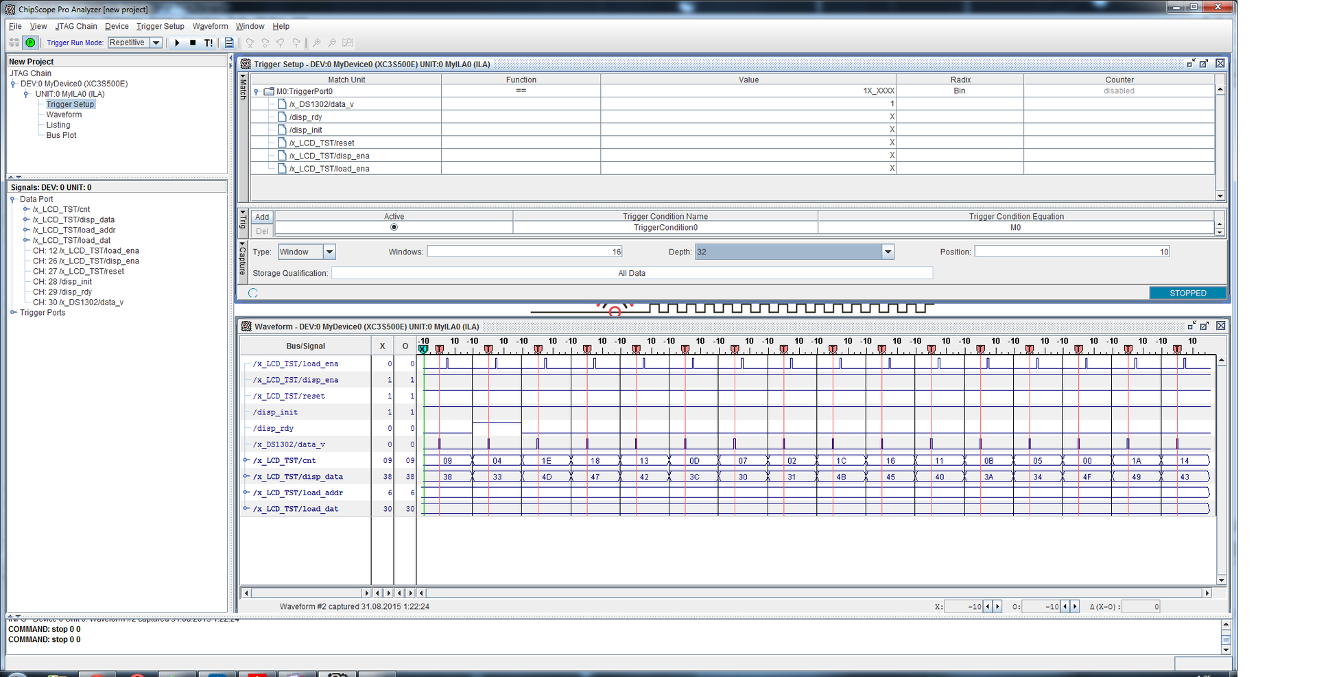
ChipScope debug process:
The source code on github is LCD Timer on FPGA .
Video demonstration of the project performance:
Do not be surprised by the date displayed on the display. The material was filmed and prepared a long time ago, and only now came to the article. Lazy to retake ... :)
Related projects:
- The project is based on the AVR microcontroller .
- Arduino based project .
Source: https://habr.com/ru/post/274843/
All Articles