Node.js in the service of an electronics developer: we create libraries of microcircuits
Hello! Today we talk about circuitry. And to make it more interesting, we will add Node.js here. The attentive reader will immediately ask, what is the connection between them? And such that we will try, using modern technologies, to make life a little easier for those who are friends with a soldering iron, who like to program Arduino / BeagleBoard all there, and generally enjoys electronics a little more than at the consumer level. In short, we will try to automate a little the process of creating a library of electronic elements.
If it became interesting, then welcome under cat.
Many of us sometimes have an overwhelming desire to develop some kind of electronic device. Whether it be a robot, a gadget, or at least a shield for Arduino, which performs specific, close to our heart functions. And it comes time to develop a printed circuit board. How does this process usually take place? We think over the necessary functionality, select the element base, roughly estimate the structural and functional scheme. Then we download and install any EDA program (EDA - Electronic Design Automation). We sculpt the concept, then we part the printed circuit board (some prefer the autotracer, but the real hardcore players recognize only handmade). We order the manufacture of the board (well, or iron ourselves), buy items, solder, launch and enjoy our new creation. Well, or suffer with it, that's how it goes.
Those for whom this process is familiar, I think, will agree that one of the dreary, routine and time-consuming operations is the creation of a library of necessary elements in the format of the EDA in which you usually work. Actually about automation of this process further and will be discussed.
')
The same attentive reader will again ask, but after all, in all modern EDA there are already built-in libraries of elements, well, in case the necessary element was not found, there is a corresponding editor within the same software package. It is hard to argue, but still the built-in libraries do not cover the whole diversity of this world, and the convenience of editors often leaves much to be desired. And if you need to draw up schemes according to GOST, then libraries rarely help you (for some reason, most Western software manufacturers blatantly ignore our standards or simply do not know about them). Often, the library, formed with love over the years, makes it difficult for you to switch to a more modern EDA package just because you have to go through this thorny path again.
And then I had a thought. Why don't we somehow describe the electronic components, and trust the generation of the library to the machine? Moreover, to provide some simple but flexible means of customizing this process so that the final library looks exactly as we want it. Ideally, so that we could control every step of the generation process with the ability to twist one or another parameter. Having done the setting once, get the result for life. Generate the library in the format of exactly the EDA program in which we wanted to work today.
This is how a project called QEDA.js was born. But before starting a detailed account of it, let’s go over the terminology.
From the developer’s point of view, an electronic radio element (ERE) generally consists of a conditional graphic designation (CRB) and a footprint on the board.
UGO (foreigners call it a schematic symbol ) is an image of an element that is used on a circuit diagram, and which allows us to distinguish a resistor from a capacitor, a microcircuit from a connector, and so on.
A footprint ( land pattern , footprint , sometimes pad layout in English terminology) is an image of the place on the board where the element will be installed physically. There is a remarkable standard IPC-7351, which regulates the calculation of the seat, depending on the body of the chip. Actually, it is used in QEDA.js.
Reference designator - the identifier of each element on the scheme / board, consisting usually of letters (characterize the class of elements) and numbers (the ordinal number of the element on a particular scheme). For example, C4 is the 4th capacitor, and the VT21 is the 21st transistor.
Pinout , or pinout, is a description of the location and purpose of an element's pins.
So, enough water, go to the point. Before you look under the hood, do a number of simple operations.
In the directory where the script was placed, the subdirectory
Now we’ll go back and try to figure out what happens when this script is executed? After connecting the QEDA.js module and creating the container object for our ERE, we add a couple of ready-made items to this container (we’ll open a veil of secrecy, in fact, these are just YAML files stored in a special repository ). When you first start the script pumps up descriptions of these items in the
However, with a probability of 99, (9)%, you will not find the component you need in the repository of ready-made elements (the fact is that it is currently in the filling stage). So we need to learn how to add our own elements.
Well, let's do it! Create a
Create a
Run:
We get:
Well, I hope I managed to interest you a little. Now dive a little deeper into the processes that are taking place.
As I mentioned above, all the necessary and sufficient information about ERE is contained in its YAML description. It reflects such parameters as:
Well, what about GOST? It's simple, we add a little script.coffee code:
We start. For comparison, we give the result “before and after” for the part of Altera 5M1270ZT144 (note that the reference designation has also changed in accordance with GOST):
Before :
After :

Well, for dessert, a couple of real, not hypothetical examples of the result of the work:
I touched only a small part of the API, so that the article did not turn out to be too long, and did not reflect the whole variety of settings and parameters that can be varied.
What remains to be done? In essence, the project is now at the stage of proof of concept. You need to make another car and a small cart. What is planned:
Github: https://github.com/qeda
If it became interesting, then welcome under cat.
Foreword
Many of us sometimes have an overwhelming desire to develop some kind of electronic device. Whether it be a robot, a gadget, or at least a shield for Arduino, which performs specific, close to our heart functions. And it comes time to develop a printed circuit board. How does this process usually take place? We think over the necessary functionality, select the element base, roughly estimate the structural and functional scheme. Then we download and install any EDA program (EDA - Electronic Design Automation). We sculpt the concept, then we part the printed circuit board (some prefer the autotracer, but the real hardcore players recognize only handmade). We order the manufacture of the board (well, or iron ourselves), buy items, solder, launch and enjoy our new creation. Well, or suffer with it, that's how it goes.
Those for whom this process is familiar, I think, will agree that one of the dreary, routine and time-consuming operations is the creation of a library of necessary elements in the format of the EDA in which you usually work. Actually about automation of this process further and will be discussed.
')
And what is the salt?
The same attentive reader will again ask, but after all, in all modern EDA there are already built-in libraries of elements, well, in case the necessary element was not found, there is a corresponding editor within the same software package. It is hard to argue, but still the built-in libraries do not cover the whole diversity of this world, and the convenience of editors often leaves much to be desired. And if you need to draw up schemes according to GOST, then libraries rarely help you (for some reason, most Western software manufacturers blatantly ignore our standards or simply do not know about them). Often, the library, formed with love over the years, makes it difficult for you to switch to a more modern EDA package just because you have to go through this thorny path again.
More specifics, Carl
And then I had a thought. Why don't we somehow describe the electronic components, and trust the generation of the library to the machine? Moreover, to provide some simple but flexible means of customizing this process so that the final library looks exactly as we want it. Ideally, so that we could control every step of the generation process with the ability to twist one or another parameter. Having done the setting once, get the result for life. Generate the library in the format of exactly the EDA program in which we wanted to work today.
This is how a project called QEDA.js was born. But before starting a detailed account of it, let’s go over the terminology.
From the developer’s point of view, an electronic radio element (ERE) generally consists of a conditional graphic designation (CRB) and a footprint on the board.
UGO (foreigners call it a schematic symbol ) is an image of an element that is used on a circuit diagram, and which allows us to distinguish a resistor from a capacitor, a microcircuit from a connector, and so on.
A footprint ( land pattern , footprint , sometimes pad layout in English terminology) is an image of the place on the board where the element will be installed physically. There is a remarkable standard IPC-7351, which regulates the calculation of the seat, depending on the body of the chip. Actually, it is used in QEDA.js.
Reference designator - the identifier of each element on the scheme / board, consisting usually of letters (characterize the class of elements) and numbers (the ordinal number of the element on a particular scheme). For example, C4 is the 4th capacitor, and the VT21 is the 21st transistor.
Pinout , or pinout, is a description of the location and purpose of an element's pins.
Meet: QEDA.js
So, enough water, go to the point. Before you look under the hood, do a number of simple operations.
- Install Node.js (if you haven't installed it yet). Details on the manufacturer's website: nodejs.org
- Install CoffeeScript (of course, you can skip this step and use vanilla JavaScript, but the following examples will be written in CoffeeScript):
npm install -g coffee-script - Install QEDA.js:
npm install -g qeda - Create a
script.coffeefile and fill it with the following lines:Qeda = require 'qeda' lib = new Qeda.Library lib.add 'Altera/5M1270ZT144' # Add Altera MAX V CPLD lib.add 'Analog/AD9393' # Add Analog Devices HDMI interface lib.add 'ST/L3GD20H' # Add STMicroelectronics gyroscope lib.add 'TI/ISO721' # Add Texas Instruments digital isolator lib.add 'TI/ISO722' # Add Texas Instruments digital isolator lib.generate 'mylib' - Run the script:
coffee script.coffee
In the directory where the script was placed, the subdirectory
kicad will appear, which actually contains the newly baked library in the format of a free, free and open EDA program called KiCad. You can download the distribution of this program from the official site: kicad-pcb.orgNow we’ll go back and try to figure out what happens when this script is executed? After connecting the QEDA.js module and creating the container object for our ERE, we add a couple of ready-made items to this container (we’ll open a veil of secrecy, in fact, these are just YAML files stored in a special repository ). When you first start the script pumps up descriptions of these items in the
library subdirectory. The last line is responsible for generating library files in KiCad format. This is the essence of our target files, for which everything was started.However, with a probability of 99, (9)%, you will not find the component you need in the repository of ready-made elements (the fact is that it is currently in the filling stage). So we need to learn how to add our own elements.
Well, let's do it! Create a
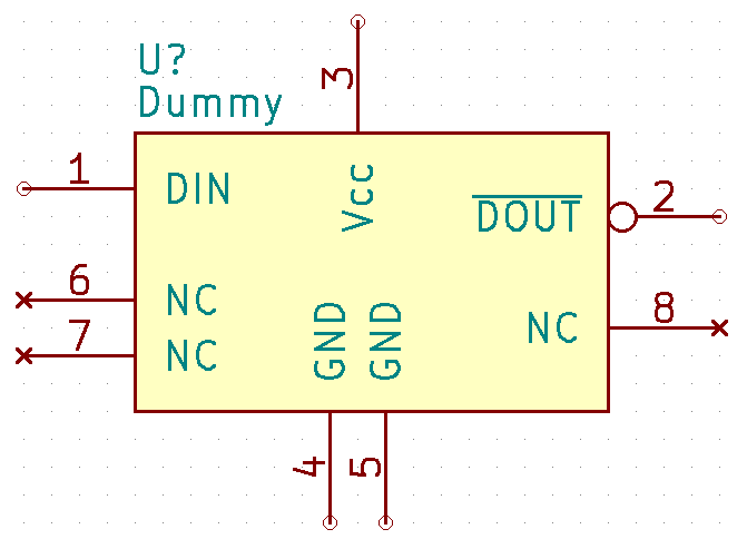
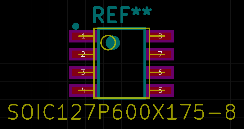
library subdirectory if it does not already exist, and in it create a dummy.yaml file with the following contents: name: Dummy pinout: DIN: 1 ~DOUT: 2 Vcc: 3 GND: 4, 5 NC: 6-8 properties: power: Vcc ground: GND in: DIN out: ~DOUT nc: NC inverted: ~DOUT schematic: symbol: IC left: DIN, NC right: ~DOUT, NC top: Vcc bottom: GND housing: pattern: SOIC outline: JEDEC MS-012 AA Create a
custom.coffee file (it should be on the same level as the library directory) and write in it: Qeda = require 'qeda' lib = new Qeda.Library lib.add 'Dummy' # Adding custom element lib.generate 'dummy' Run:
coffee custom.coffee We get:
Well, I hope I managed to interest you a little. Now dive a little deeper into the processes that are taking place.
As I mentioned above, all the necessary and sufficient information about ERE is contained in its YAML description. It reflects such parameters as:
- Pinout - pin names and corresponding numbers. Numbers can be listed separated by commas or given a range, and these two options can be combined. Example:
pinout: DATA: 1, 3-6, 10
Numbers may contain letters (for example, for BGA):pinout: GND: B1, C10-C13, AA1-AC3
You can also combine several conclusions into a group:pinout: SPI: CS: 1 CLK: 2 MOSI: 3 MISO: 4
You can also group the names of the outputs, they are automatically converted into a list (their number must match the number of numbers on the right):pinout: D16-0, CLK: 1-18 - Properties of the findings ( properties ) - strictly speaking, this is also part of the pinout, but not necessarily. Allows you to shed some light on the type of findings. This information is used by many EDA programs both to display a symbol and to conduct some checks (for example, so that you do not allow power to the ground leg).
properties: power: Vcc # ground: GND # in: DIN # out: ~DOUT # nc: NC # inverted: ~DOUT # - Description of the UGO ( schematic ) - specify the script responsible for drawing the element, plus some settings for how the symbol should look.
schematic: symbol: IC # 'ic.coffee' left: DIN, NC # right: ~DOUT, NC # ('NC' ) top: Vcc # bottom: GND # - Description of the case ( housing ) - we give the dimensions of the case or a link to a file with standard sizes, and also specify the script that will draw the footprint.
housing: pattern: SOIC # 'soic.coffee' outline: JEDEC MS-012 AA # 'jedec/ms-012.yaml', 'AA'
But you can set dimensions directly from the datasheet:housing: pattern: SOIC # 'soic.coffee' pitch: 1.27 # bodyWidth: 3.80-4.00 # bodyLength: 4.80-5.00 # height: 1.75 # leadSpan: 5.80-6.20 # ( ) leadLength: 0.40-1.27 # leadWidth: 0.31-0.51 # leadCount: 8 #
Well, what about GOST? It's simple, we add a little script.coffee code:
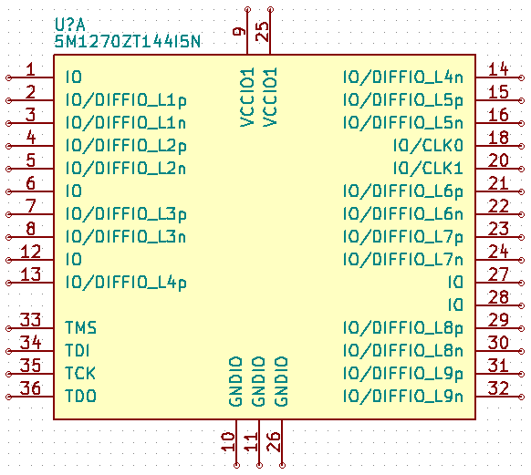
Qeda = require 'qeda' lib = new Qeda.Library symbol: style: 'GOST' lib.add 'Altera/5M1270ZT144' # Add Altera MAX V CPLD lib.add 'Analog/AD9393' # Add Analog Devices HDMI interface lib.add 'ST/L3GD20H' # Add STMicroelectronics gyroscope lib.add 'TI/ISO721' # Add Texas Instruments digital isolator lib.add 'TI/ISO722' # Add Texas Instruments digital isolator lib.generate 'mylib' We start. For comparison, we give the result “before and after” for the part of Altera 5M1270ZT144 (note that the reference designation has also changed in accordance with GOST):
Before :
After :
Well, for dessert, a couple of real, not hypothetical examples of the result of the work:
Analog Devices AD9393
ad9393.yaml:
UGO:

Seat:

name: AD9393 description: Low power HDMI display interface pinout: PD: B9 VIDEO: Rx0+: K5 Rx0-: K4 Rx1+: K8 Rx1-: K7 Rx2+: J10 Rx2-: K10 RxC+: K2 RxC-: K1 OUTPUTS: D23-0: B6, A6, B5, A5, B4, A4, B3, A3-A1, B1-H2 DCLK: A7 HSOUT: A8 VSOUT: B8 O/E: A9 FILT: D10 Vd: E7, F7 Vdd: D4, D5 PVdd: F9, G9 DVdd: G6, G7 GND: C9, C10, D6, D7, D9, E4, E9, E10, F4, H10, J1, K3, K6, K9 CONTROL: SCL: B10 SDA: A10 HDCP: DDC_SCL: H9 DDC_SDA: J9 MCL: G10 MDA: F10 AUDIO: S/PDIF: J7 I2S0-3, MCLK: J6-J2 SCLK: G4 LRCLK: G5 DE: B7 RTERM: J8 properties: in: PD, Rx0+, Rx0-, Rx1+, Rx1-, Rx2+, Rx2-, Rx3+, Rx3-, RxC, RxC, SCL, DDC_SCL, MCL, DE out: D23-0, DCLK, HSOUT, VSOUT, O/E, S/PDIF, I2S0-3, MCLK, SCLK, LRCLK bidir: SDA, DDC_SDA, MDA power: Vd, Vdd, PVdd, DVdd ground: GND analog: FILT, RTERM schematic: symbol: IC left: PD, VIDEO, FILT, CONTROL, HDCP, AUDIO, DE right: OUTPUTS, RTERM top: Vd, Vdd, PVdd, DVdd bottom: GND housing: pattern: BGA pitch: 0.5 rowCount: 10 columnCount: 10 leadCount: 76 lead: 0.25-0.35 bodyWidth: 5.90-6.10 bodyLength: 5.90-6.10 height: 1.40 keywords: IC, digital, receiver, converter UGO:
Seat:
STMicroelectronics L3GD20H
l3gd20h.yaml:
UGO:

Seat:

name: L3GD20H description: Three-axis digital output gyroscope pinout: Vdd_IO: 1 I2C: SCL: 2 SDA: 3 SA0: 4 SPI: SPC: 2 SDI: 3 SDO: 4 3WIRE: SDO: 3 CS: 5 DRDY: 6 INT: INT1: 7 INT2: 6 DEN: 8 RES: 9-11, 15 GND: 12, 13 Cap: 14 Vdd: 16 properties: power: Vdd_IO, Vdd ground: GND, RES in: CS, DEN out: INT1-2, SCL, SDO bidir: SDA analog: Cap schematic: symbol: IC left: CS, I2C, DEN right: INT, RES, Cap top: Vdd_IO, Vdd bottom: GND housing: pattern: QFN pitch: 0.5 bodyLength: 2.85-3.15 bodyWidth: 2.85-3.15 height: 1 pullBack: 0.1 rowCount: 5 columnCount: 3 leadLength: 0.29-0.41 leadWidth: 0.19-0.31 UGO:
Seat:
Conclusion
I touched only a small part of the API, so that the article did not turn out to be too long, and did not reflect the whole variety of settings and parameters that can be varied.
What remains to be done? In essence, the project is now at the stage of proof of concept. You need to make another car and a small cart. What is planned:
- Expand the number of supported item types
- Deepen the diagnosis of erroneous situations
- Go all the way to making the board
- Generate 3D Models
- Support formats and other EDA programs
- Finally, all this is well documented.
Source
Github: https://github.com/qeda
Source: https://habr.com/ru/post/271051/
All Articles