Video transmission at frequencies up to 100 MHz in PC
Video transmission at frequencies up to 100 MHz in PC
Introduction
Our department is engaged in the development of CCD matrices and lines. For each sensor developed, it is necessary to create a photodetector (FPU), which will allow it to be tested, to calculate the device parameters - dynamic range, unevenness of the output signal, level of generation-recombination dark current, etc.
The FPU is a kind of video camera, but not one that you can simply take in your hand and go to the park to shoot something (for example, a squirrel).
Photodetector usually consists of several boards. On one board are power stabilizers, filters, and on the other (or others), the entire microcircuit stuffing. In the center of the main board is the sensor itself, around it are powerful fast keys for supplying control voltages to the CCD electrodes. The emitter follower is connected to the output of the device, then a video processor (smart ADC for CCD) goes and completes all the FPGAs. She delivers the sync pulses to the CCD through the keys, clocks the video processor, takes the digital code from it and, after the necessary processing, sends it to the output connector. In addition to one code, sync pulses are output - PCLK (pixel synchronization), HSYNC (horizontal sync signal), VSYNC (frame synchronization), which are necessary for normal reception of information on the receiving side.
')
Of course, the FPU should introduce as little noise as possible into the analog signal from the CCD in order to obtain good design parameters of the device. But the article is not about FPU and not about the CCD, but about using and how you can transmit a digital code at high frequencies to a PC.
Brief Description of Transmitter Chip
A few years ago it became necessary to transfer a digital video stream from a matrix with the number of elements 1000x1000 (the matrix of our development). Prior to this, we used only rulers (again - our development) and used USB 2.0 in Hi-Speed mode to transfer data. There was enough speed for the rulers, there were no problems. But on the horizon, the task to send 12bit loomed. 40MHz stream. From simple calculations, it is clear that 40MHz * 12bit = 480Mbit / s. - this is the limit of USB2.0 HI-SPEED, besides also a theoretical one. We took the path of least resistance, in the neighboring department we asked for a fiber optic transmission system, we launched it and it all worked. But I wanted versatility in a bundle of FPU-PCs, especially since the fiber optic transmitter was designed for a PCI bus, which is almost sunk into oblivion.
While this bundle for transmission worked, we were looking for solutions based on USB3.0 bus. The quest was crowned with success, the solution turned out to be the chip - EZ-USB FX3 SuperSpeed USB 3.0 peripheral controller from Cypress. Functional diagram of the controller is shown in Figure 1.
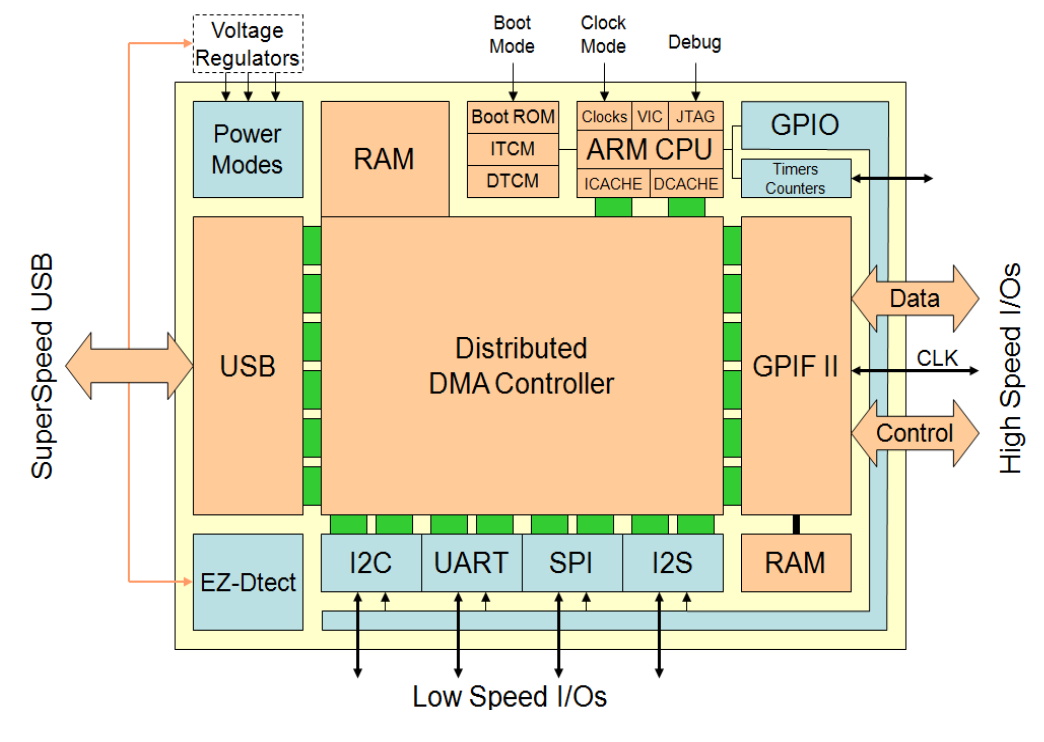
Figure 1 - The functional diagram of the controller
This controller has a configurable GPIF II interface. With it, you can connect the FPGA, the memory, the required processor, etc. to the chip ... The whole point of this interface is that you can configure it as you like. At its disposal 32-bit. data bus, 8-bit address bus and a large number of synchronization lines. It is not necessary to use GPIF II to its fullest; you can limit yourself to a smaller data bus, remove the address bus, and use the empty legs for other purposes. The maximum frequency of the interface - 100MHz. Its programming takes place in a special software - GPIF II Designer. Writing the main firmware comes in an environment from Cypress based on Eclipse.
As a core ARM926EJ works at 200 MHz. EZ-USB FX3 does not have flash memory, the program is loaded into SRAM from external Flash, EEPROM or via USB3.0 from a PC. SRAM capacity and number of GPIF II data lines depend on the controller model. The maximum size of RAM is 512kB, and the minimum is 256kB. Debugging is done via JTAG. In addition to GPIO, the controller has a standard set of interfaces - SPI, I2C, UART, I2S. Also in the chip is implemented DMA-controller. The cases are represented by the following types - 121-foot BGA and 131 pin WLCSP.
The principle of transferring video data using EZ-USB FX3
Initially I planned to give as an example a bunch of FPU - a PC on a domestic matrix of 1000x1000 elements with parsing the creation of firmware for the GPIF II interface and the controller itself, but did not do that, too much would need to be written for one article. Moreover, Cypress has a very good example for an HD matrix by which you can deal with the work of the m / scheme when transmitting video data.
So, the whole cascade of data transfer:
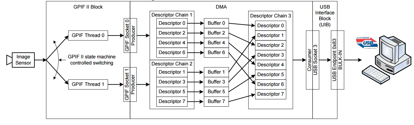
Figure 2 - Video Data Cascade
1) GPIF II interface . It works in two-threaded mode, each stream is connected to its socket. A socket is a connection point between the various peripherals of the controller, as well as the peripherals and the processor. Producer Socket is the socket through which data is written, Consumer Socket is the socket through which data is read. Dual streaming mode (Ping-Pong) allows you to write data to the buffer without delay. When the zero buffer fills when the zero stream is working, it will automatically switch to another stream and write to the new buffer, and the old one will be sent to the PC. The absence of delays allows you to transmit a video signal in real time, limited to a small amount of memory.
2) DMA block . In this example, 8 buffers are used for receiving and transmitting data. Arrays can be 8, 16 or 32 bit. The depth of the arrays depends on the specific task. You can use a different number of buffers, the main thing is that they are of the same bit depth and volume and that their total volume does not crawl out of the available memory. The description of each buffer is stored in its descriptor - Descriptor [7: 0]. All eight descriptors are divided into two groups (Descriptor Chain 1 and 2). Each of the two groups is connected to its own recording socket.
The chain of descriptors 3 refers to the USB controller and serves for the orderly reading of data via USB Socket 3 from buffers 7-0.
As you can see, there is no CPU block in the figure. Its absence is not accidental, since if there is no need to process the transmitted data, then the kernel can not be used and transmit data directly.
When transmitting data without processing, the receiving party in the form of a PC receives a sausage with information without identification marks. The first received element is taken as the synchronization starting point and counts pixels, lines and frames from this element. Knowing the number of pixels in a line and the number of lines in a frame, this can be turned. It turns out asynchronous synchronization, the thing is not very pleasant. It is desirable that the data come already numbered.
This is where the ARM9 core comes in, which allows you to implement software synchronization. When initializing DMA arrays, it is necessary to reserve space in each buffer for a special header (for example, 16 bytes). These 16 bytes will never be filled with video data. When the buffer is full, the DMA controller will signal this to the processor, and the processor, in turn (with your help), will take and write the necessary data in the header. After processing the header, the processor will give a command to transfer the buffer to the PC.
For a more complete description of the principle of operation of the controller when transferring video data, I recommend reading this guide - “Cypress” for how to implement an Image Sensor Interface EZ-USB FX3 in a USB. It describes in detail the process of creating firmware for GPIF II. After parsing the manual, you can download a companion project under Eclipse for the controller itself and deal with it.
The article turned out to be introductory and uninformative from a practical point of view. If you want to look at the process of programming GPIF II and MK then write in the comments, I will try to write everything down. As an example, I will analyze the firmware for the domestic line of 12 thousand elements.
Source: https://habr.com/ru/post/270733/
All Articles