Altera + OpenCL: we open the core

Hello!
In the last article, I launched a simple OpenCL example on Altera's FPGA:
// ACL kernel for adding two input vectors __kernel void vector_add( __global const uint *restrict x, __global const uint *restrict y, __global uint *restrict z ) { // get index of the work item int index = get_global_id(0); // add the vector elements z[index] = x[index] + y[index]; } I deliberately did not go into details and showed the tip of the iceberg: the development process, the assembly of the project, the launch on the system.
')
During the preparation of the first article, it became wildly interesting to me what these lines turn into (from the FPGA). Understanding the architecture will enable something to optimize and understand what resources are going for, as well as what is good and bad for this system.
In this article we will try to open the core and find answers to the following questions:
- What is its architecture?
- How is it configured? How to get the data for processing?
- At what frequency does it work? How is this determined?
- Is it possible to simulate only the core in RTL simulators?
- What blocks occupy the most resources? Is it possible to somehow optimize it?
Let's take a look at his insides! Welcome under the cut!
How does Altera see it
Before intently studying the project for FPGA, let's turn to various presentations from the vendor: what do they tell about the implementation in a high-level (marketing) language.
I recommend to look a great presentation, introduction to OpenCL from Altera
Harnessing the Power of FPGAs using Altera's OpenCL Compiler ( carefully , more than a hundred slides, ~ 16 MB).
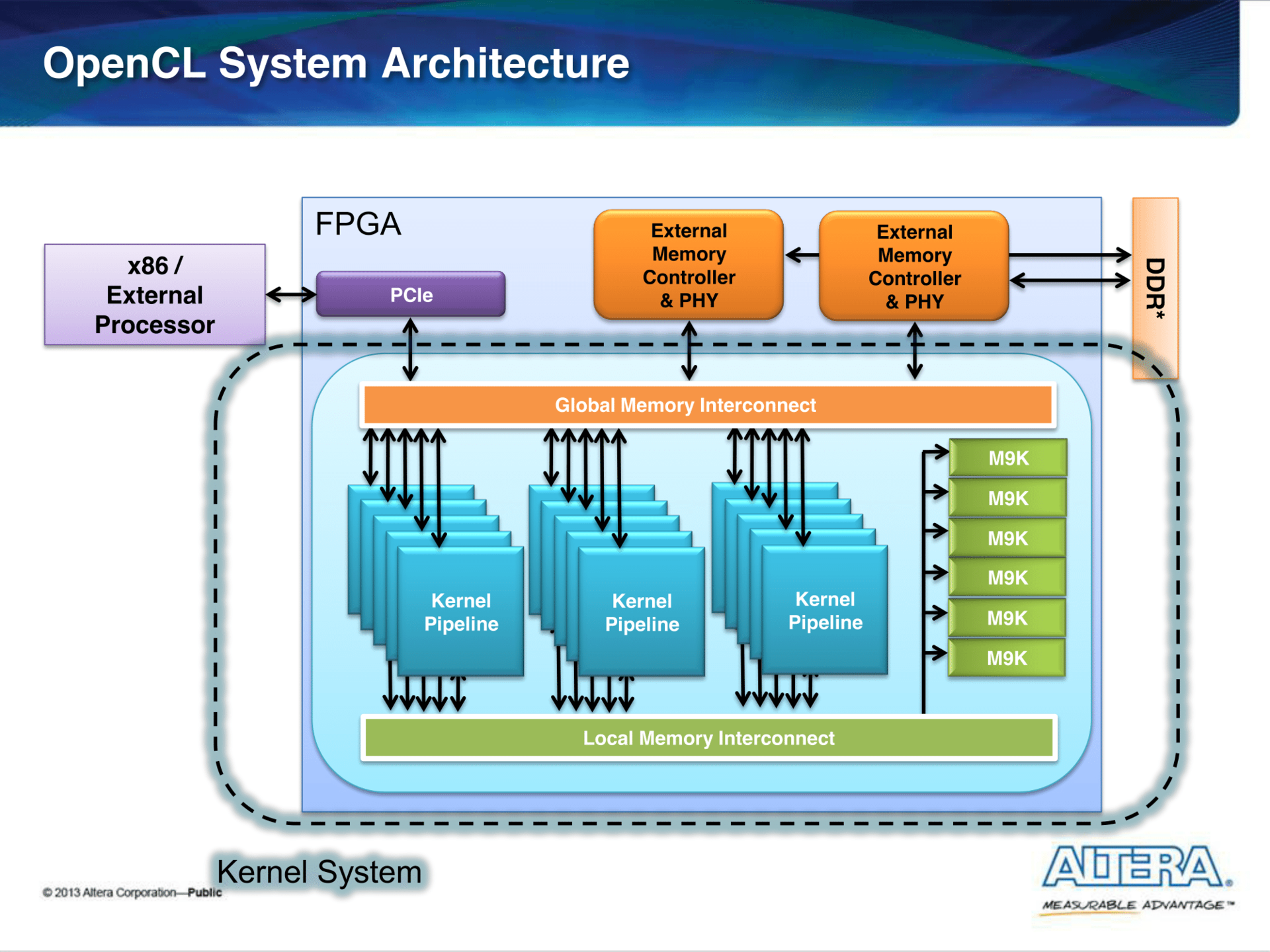
The firmware consists of:
- IP cores that provide access to the periphery (PCIe, external memory (DDR, QDR)).
- The kernels realized by the principle of the conveyor. They are computed, described in the OpenCL kernels.
- Infrastructure: Global and Local Memory Interconnect .
Interconnect is the division of a common bus between modules that are masters and slaves (master and slave).
In our case, wizards are the cores that read / write data in both global memory (this can be either host memory or external memory) or local (internal) memory, which can be called a cache. As a result of the process of arbitration and multiplexing of data, modules appear, which, as we will see below, can consume a significant amount of resources.
For convenience, the communication protocol between modules is standardized. Altera uses Avalon- type interfaces in its projects: Avalon-MM (Memory Mapped) and Avalon-ST (Streaming). I will not dwell on this in detail: the reader can independently read about it here . In this article, most of the interconnect will be the Avalon-MM interface.
Once again I will emphasize that all this is obtained automatically from the kernel description on OpenCL.
Post update results
In the last article I described the build results based on the work on the Quartus 14.1 version.
Version 15.1 was released not long ago, and I decided to see if there were any big differences. To do this, I regenerated the source and rebuilt them with a new version.
Alas, in the OpenCL visualizer and profiler there were no changes (seemingly): their appearance still leaves much to be desired.
Build report with --profile (with profiling counters):
+-----------------------------------------------------------------------------------+ ; Fitter Summary ; +---------------------------------+-------------------------------------------------+ ; Fitter Status ; Successful - Sun Nov 22 13:18:14 2015 ; ; Quartus Prime Version ; 15.1.0 Build 185 10/21/2015 SJ Standard Edition ; ; Family ; Cyclone V ; ; Device ; 5CSEMA5F31C6 ; ; Timing Models ; Final ; ; Logic utilization (in ALMs) ; 5,472 / 32,070 ( 17 % ) ; ; Total registers ; 10409 ; ; Total pins ; 103 / 457 ( 23 % ) ; ; Total block memory bits ; 127,344 / 4,065,280 ( 3 % ) ; ; Total RAM Blocks ; 44 / 397 ( 11 % ) ; ; Total PLLs ; 2 / 6 ( 33 % ) ; ; Total DLLs ; 1 / 4 ( 25 % ) ; +---------------------------------+-------------------------------------------------+ Compared with the previous version of the compiler, the project has lost approximately 100 ALM.
But the assembly report without profiling counters:
+-----------------------------------------------------------------------------------+ ; Fitter Summary ; +---------------------------------+-------------------------------------------------+ ; Fitter Status ; Successful - Sun Nov 22 13:51:21 2015 ; ; Quartus Prime Version ; 15.1.0 Build 185 10/21/2015 SJ Standard Edition ; ; Family ; Cyclone V ; ; Device ; 5CSEMA5F31C6 ; ; Timing Models ; Final ; ; Logic utilization (in ALMs) ; 4,552 / 32,070 ( 14 % ) ; ; Total registers ; 7991 ; ; Total pins ; 103 / 457 ( 23 % ) ; ; Total block memory bits ; 127,344 / 4,065,280 ( 3 % ) ; ; Total RAM Blocks ; 44 / 397 ( 11 % ) ; ; Total PLLs ; 2 / 6 ( 33 % ) ; ; Total DLLs ; 1 / 4 ( 25 % ) ; +---------------------------------+-------------------------------------------------+ As you can see, about 1000 ALM occupy the profiling counters and logic that "reads" them.
In the future, it is this report that we will use to analyze what it takes.
First look at the project
Let me remind you that the project is laid out on a githaba .
The project file is called straightforwardly: top.qpf (QPF - Quartus Project File), the most important module is top.v , which in fact contains an instance of the system module and a simple counter that is displayed on the LEDs.
system (4535 ALM)
system is an auto-generation module using Qsys . Qsys is a GUI-ishna tool that allows you to connect different IP blocks, automatically generating the code for the modules that are needed for the interconnect, switching from one frequency to another, etc.
Modules:
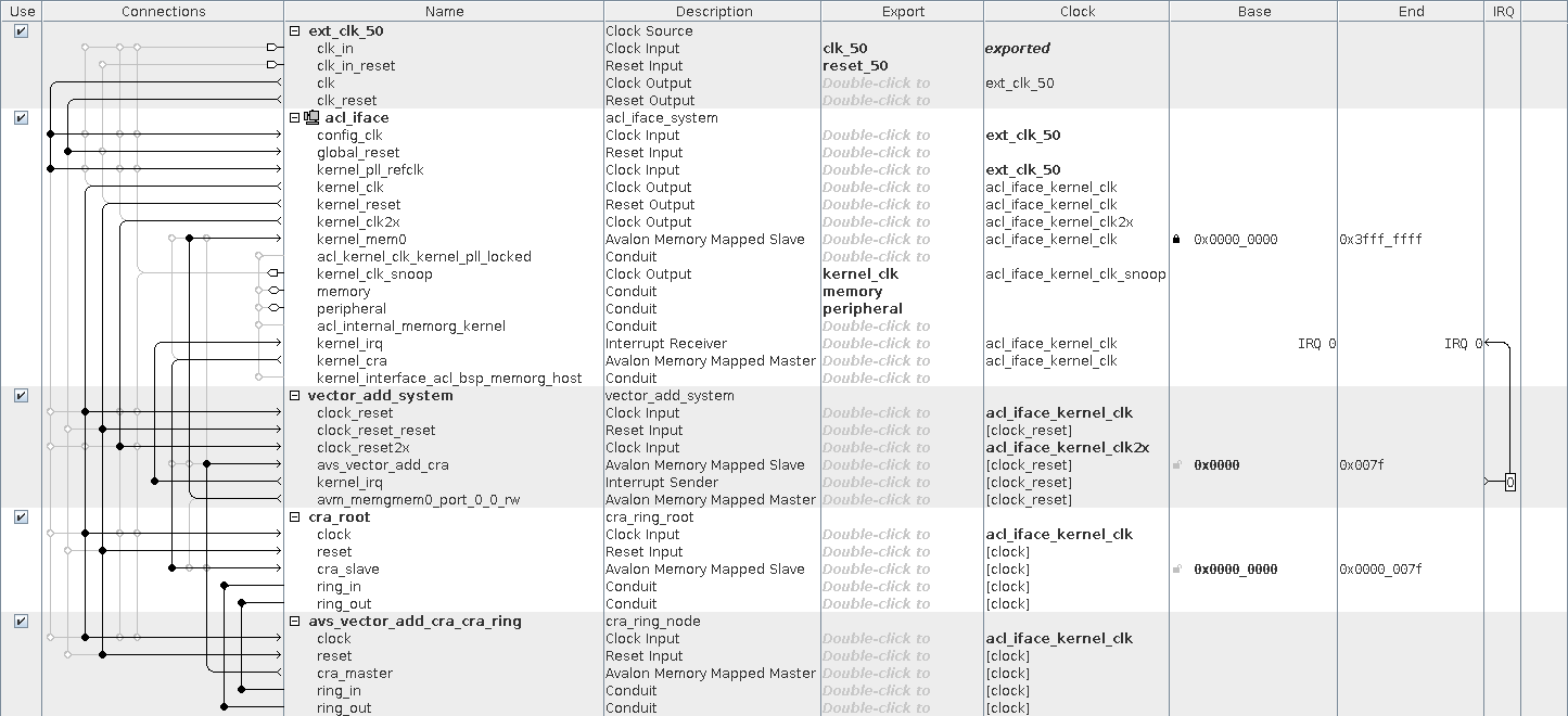
- vector_add_system (2141 ALM) is a module that implements what we wrote in the vector_add core.
- acl_iface (2343 ALM) is an infrastructure that provides more convenient access and interaction with the kernel.
Interfaces:
- avs_vector_add_cra - Avalon-MM for managing the kernel.
- avm_memgmem0_port_0_0_rw - Avalon-MM for accessing DDR memory. The data width is 256 bits.
acl_iface (2343 ALM)
Modules:
- pll (0 ALM) : PLL that receives a clock pll_outclk0 (100 MHz) from config_clk (50 MHz, comes from an external oscillator).
- acl_kernel_clk (1057 ALM) : another PLL: it generates a shred that is sent to the kernel. It has an interesting nuance: we'll talk about it in more detail later.
- acl_kernel_interface (439 ALM) : provides the "interaction" of the core and the processor (via the control interface and interrupt).
- clock_cross_kernel_mem1 (82 ALM) : he is engaged in the "coordination" of interfaces that operate at different frequencies ( CDC ).
- hps (0 ALM) : this is a HPS instance (Hard Processor System). No logic in the FPGA, he does not take, because this is the hardware core.
Interfaces:
- f2h_sdram0 - Avalon-MM interface for accessing DDR memory. The data width is 256 bits, and the operating frequency is pll_outclk0 (100 MHz).
- h2f_lw - AXI interface. Through it, the CPU (ARM) has the ability to manage and configure the system using the control / status registers of the kernel, etc.
If we add up the total capacity of these modules, the amount will not converge. The fact is that Qsys does not show interconnect modules by default. To display them, you must click Show System With Qsys Interconnect in the System menu. After that you can see that there are modules of the form mm_interconnect_ * , which occupy 568 and 195 ALM.
vector_add_system (2141 ALM)
The architecture of this module cannot be viewed in the GUI: to understand how it works, we dive into Verilog.
An approximate diagram looks like this:
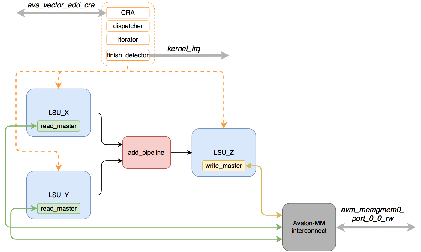
- vector_add_system_interconnect_ * (443 ALM) - interconnect modules that conduct arbitration and multiplexing of the avm_memgmem0_port_0_0_rw interface
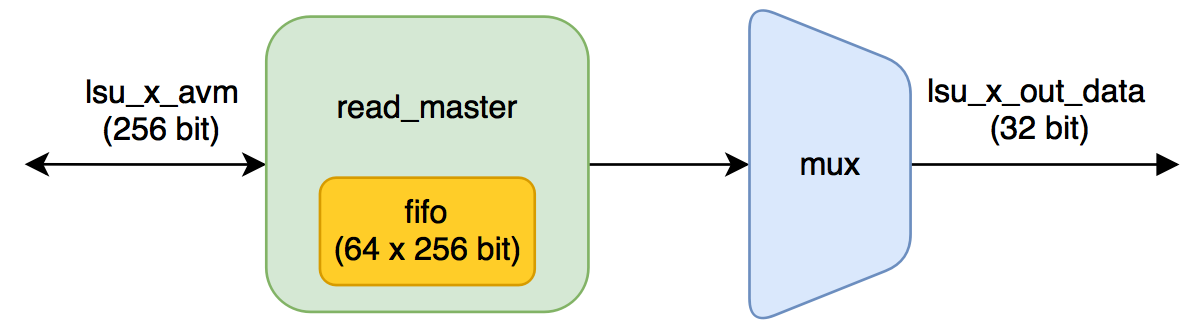
- LSU_X (235) , LSU_Y (239) - read data from global memory for vectors (kernel arguments x and y, respectively).
- LSU_Z (424 ALM) - writes the result of the calculations to global memory (argument z ).
- acl_id_iterator (228 ALM) , acl_work_group_dispatcher (149 ALM) - they issue a task to be performed by the kernel (they show which element should be processed).
- acl_kernel_finish_detector (144 ALM) - determines when the kernel has finished its work.
Note:
LSU modules are instances of a single module ( lsu_top ) and are named lsu_local_bb0_ld_ , lsu_local_bb0_ld__u0 and lsu_local_bb0_st_add . For convenience, I gave them more "humane" names. We'll talk more about LSU below.
How the kernel works:
- There is a setup through CRA, processing is started.
- LSU_X and LSU_Y receive “commands” to read the data and make requests to the global memory.
- The read data is buffered in memory ( FIFO ) until data from both LSUs are ready.
- As soon as the data is in both FIFOs, they are sent to the pipeline that performs the addition.
- The result is in LSU_Z , where they wait for the opportunity to be written to global memory.
- As soon as the desired number of elements is processed, and all the results are recorded in memory (there are no pending entries), the kernel_finish_detector is triggered — the kernel_irq interrupt is set .
It is important to note that the three LSUs will fight among themselves for a single access interface to the global memory - they are masters of the Avalon-MM interface.
The conveyor, which I designated in the scheme as add_pipeline , is actually not placed in a separate module: it is simply located in the vector_add.v file in the vector_add_basic_block_0 module.
The line itself, which adds up two 32-bit numbers, looks like this:
assign local_bb0_add = (rstag_3to3_bb0_ld__u0 + rstag_3to3_bb0_ld_); The logical elements that will be created from this line and do all the useful work.
All the rest is the infrastructure that drives the data to this logic.
LSU (Load Store Unit)
The most interesting module of this kernel is LSU. Let's see how it works.
lsu_top is in fact a wrapper over other lsu_ * -modules, which are selected depending on the parameters READ and STYLE .
Of all the varieties, we will have only two:
- LSU_READ_STREAMING - LSU_X , LSU_Y (READ = 1, STYLE = "STREAMING")
- LSU_WRITE_STREAMING - LSU_Z (READ = 0, STYLE = "STREAMING")
LSU_READ_STREAMING
Pay attention to the parameters of the module:
BURSTCOUNT_WIDTH = 5; MEMORY_SIDE_MEM_LATENCY = 89; BURSTCOUNT_WIDTH shows the width of the avm_burstcount signal - when queried by the Avalon-MM interface, the number of words that must be read during the transaction is located there .
If the signal width is equal to five, then the maximum value of the wave is equal to 16. This clearly follows from the specification :
The value of the maximum burstcount parameter must be a power of 2. A burstcount interface of width n can encode a max burst of size 2^(n-1). For example, a 4-bit burstcount signal can support a maximum burst count of 8. The minimum burstcount is 1. This means that a maximum of 16 256-bit words will be read in a single request — these are 4096 Kbit or 128 32-bit numbers (we add 32-bit integers).
MEMORY_SIDE_MEM_LATENCY affects the number of FIFO words in lsu_burst_read_master . This FIFO is used to buffer readable data from global memory.
How is the number of words for it determined:
localparam MAXBURSTCOUNT=2**(BURSTCOUNT_WIDTH-1); // Parameterize the FIFO depth based on the "drain" rate of the return FIFO // In the worst case you need memory latency + burstcount, but if the kernel // is slow to pull data out we can overlap the next burst with that. Also // since you can't backpressure responses, you need at least a full burst // of space. // Note the burst_read_master requires a fifo depth >= MAXBURSTCOUNT + 5. This // hardcoded 5 latency could result in half the bandwidth when burst and // latency is small, hence double it so we can double buffer. localparam _FIFO_DEPTH = MAXBURSTCOUNT + 10 + ((MEMORY_SIDE_MEM_LATENCY * WIDTH_BYTES + MWIDTH_BYTES - 1) / MWIDTH_BYTES); // This fifo doesn't affect the pipeline, round to power of 2 localparam FIFO_DEPTH = 2**$clog2(_FIFO_DEPTH); _FIFO_DEPTH = 16 + 10 + ((89 * 4 + 32 - 1)/32) = 39 , : FIFO_DEPTH = 64 Conclusion :
A buffer (cache) of 64 words of 256 bits will be allocated.
In fact, to fix this fact, it was not necessary to pick the source: just look at the RAM Summary section of the report from the build. Our calculation turned out to be correct, and the report shows that 7 M10K blocks will be used. Seven blocks is 10240 bits * 7 = 70 Kbps, instead of the expected 256 bits * 64 = 16 Kbps.
Why did it happen?
In FPGA, internal memory is a lot of small blocks that can be configured differently.
You can see how to configure the M10K block (namely, it forms the basis of the Cyclone V chip family) here .
The maximum word length in a memory block is 40 bits, if you need to create a word in 256 bits, then you need 256/40 = 6.4 -> 7 blocks, which turned out. Due to the fact that the number of words in memory is 64, each block will be configured as 64x40, and the remaining 75% of memory will simply not be used.
What affects the size of the bursts and the size of the cache?
- The more birst, the more we can read in one request, but at the same time the remaining requests to the memory will be blocked (we have three masters who want to communicate with external memory).
- The larger the cache, the more data there is in the "stock" for processing while a new piece of data is being read. I do not know the minuses of the larger cache, except for the consumption of resources. In this case, it was possible to make a cache with the number of words equal to 256 and the same number of M10K blocks would be spent.
LSU_WRITE_STREAMING
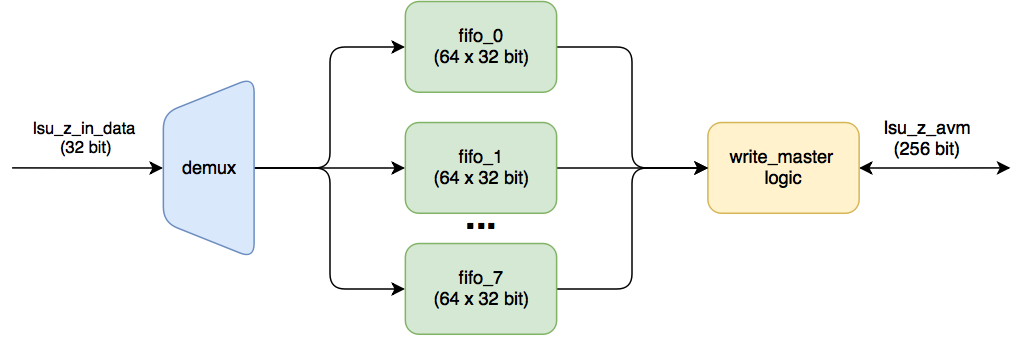
The incoming 32-bit data (the result of addition) are put in turn into their FIFO. As soon as MAXBURSTCOUNT is typed in each of them (for this module this parameter is also equal to 16), then a write-to-memory transaction occurs. Each of these FIFOs has a data width of 32. There are eight such FIFOs (256/32).
What is the amount of data calculated these fifoshki
Calculation take from the code lsu_streaming_write . For this module parameter. MEMORY_SIDE_MEM_LATENCY is 32.
localparam MAXBURSTCOUNT=2**(BURSTCOUNT_WIDTH-1); localparam __FIFO_DEPTH=2*MAXBURSTCOUNT + (MEMORY_SIDE_MEM_LATENCY * WIDTH + MWIDTH - 1) / MWIDTH; localparam _FIFO_DEPTH= ( __FIFO_DEPTH > MAXBURSTCOUNT+4 ) ? __FIFO_DEPTH : MAXBURSTCOUNT+5; // This fifo doesn't affect the pipeline, round to power of 2 localparam FIFO_DEPTH= 2**($clog2(_FIFO_DEPTH)); MAXBURSTCOUNT = 2^4 = 16 __FIFO_DEPTH = 2 * 16 + ( 32 * 32 + 256 - 1)/256 = 36 + 5 = 41 _FIFO_DEPTH = 41 : FIFO_DEPTH = 64 We confirm with the report: 64 * 32 = 2048 bits (1 M10K).
Since the FIFO is completely separate, one M10K block is allocated to each FIFO, which results in 8 M10K blocks, versus 7 M10K blocks in lsu_read_streaming .
Why did 8 FIFO, although it was possible to make one, but wide? Most likely this is easier to do (do not separately store the number of valid words).
How are LSU parameters calculated?
Let's try to figure out where such numbers came from:
There is a suspicion that these settings are taken from a file that describes the board (altera / 15.1 / hld / board / de1soc / de1soc_sharedonly / board_spec.xml) .
Find the line that is associated with the global memory:
<!-- One DDR3-800 DIMM, 256-bit data --> <global_mem max_bandwidth="6400"> <interface name="acl_iface" port="kernel_mem0" type="slave" width="256" maxburst="16" latency="240" address="0x00000000" size="0x40000000"/> </global_mem> For an explanation of these parameters, refer to the Altera SDK for OpenCL: Custom Platform Toolkit User Guide , XML Elements, Attributes, and Parameters chapter in the board_spec.xml File .
max_bandwidth - the current configuration. The Altera Offline Compiler is suitable for the application and the board. Compute this bandwidth value from datasheets of your memories.
Transfer
max_bandwidth - The maximum bandwidth of all interfaces for global memory. Altera Offline Compiler uses max_bandwidth to select the architecture that is best suited for a particular card and application. Calculate these values based on the parameters of the memory used.
Unfortunately, there are no explanations in which units and how it counts: on the one hand, the profiler wrote 6400 MB / s, on the other hand, according to calculations of 6400 MB / s, nothing is obtained: 400 (MHz, DDR clock frequency) * 32 (bit, width data signal on DDR-interface) * 2 (work on two fronts) = 25600 Mb / s = 3200 MB / s. Or should be considered in both directions?
max_burst - Maximum burst size for the slave interface.
Transfer
max_burst - The maximum burstsize for the slave (slave) interface.
In our case - 16, which gives BURSTCOUNT_WIDTH = 5. But why 16, exactly? The fpga2hps_sdram interface supports max_burstcount = 128. 16 - is this some kind of magic number, fits all? :)
latency - anonymous integer The card reads the card. For example, the Altera DDR3 memory controller running at 200 MHz with clock-crossing bridges has a latency of approximately 240 ns.
Transfer
latency - An integer that indicates the time in nanoseconds required
memory interface for the answer. The delay is the time from the read request to the receipt of data in the kernel. For example, the Altera DDR3 controller, operating at 200 MHz in conjunction with a module for switching to another frequency, has a delay of about 240 ns.
memory interface for the answer. The delay is the time from the read request to the receipt of data in the kernel. For example, the Altera DDR3 controller, operating at 200 MHz in conjunction with a module for switching to another frequency, has a delay of about 240 ns.
Suppose that in our case there is also a delay of 240 ns. Obviously, the dimension of MEMORY_SIDE_MEM_LATENCY is the number of ticks (and the comment suggests: Latency in cycles between LSU and memory ).
We will conduct several experiments, changing the values in board_spec.xml ( maxburst , latency ) and the core structure (the number of arguments that are added ( readers )). We follow the value of the MEMORY_SIDE_MEM_LATENCY parameter for both modules ( LSU_X (lsu_read_streaming) and LSU_Z (lsu_write_streaming)).
|--------------------------------------------------------| | maxburst | latency | readers | MEMORY_SIDE_MEM_LATENCY | | | | |-------------------------| | | | | LSU_X | LSU_Z | |--------------------------------------------------------| | 16 | 0 | 1 | 25 | 16 | | 16 | 100 | 1 | 45 | 16 | | 16 | 240 | 1 | 73 | 16 | |--------------------------------------------------------| | 16 | 0 | 2 | 41 | 32 | | 16 | 100 | 2 | 61 | 32 | | 16 | 240 | 2 | 89 | 32 | |--------------------------------------------------------| | 16 | 0 | 3 | 57 | 48 | | 16 | 100 | 3 | 77 | 48 | | 16 | 240 | 3 | 105 | 48 | |--------------------------------------------------------| | 32 | 0 | 1 | 41 | 32 | | 32 | 100 | 1 | 61 | 32 | | 32 | 240 | 1 | 89 | 32 | |--------------------------------------------------------| | 32 | 0 | 2 | 73 | 64 | | 32 | 100 | 2 | 93 | 64 | | 32 | 240 | 2 | 121 | 64 | |--------------------------------------------------------| | 32 | 0 | 3 | 105 | 96 | | 32 | 100 | 3 | 125 | 96 | | 32 | 240 | 3 | 153 | 96 | |--------------------------------------------------------| What dependences are traced:
- With increasing latency and fixing maxburst and readers LSU_X_MEMORY_SIDE_MEM_LATENCY increases by a value equal to latency / 5. Most likely 5 is 5 ns (are we sent to the magic frequency of 200 MHz?).
- As the number of readers increases, LSU_X_MEMORY_SIDE_MEM_LATENCY increases by the value of the birst.
- LSU_Z_MEMORY_SIDE_MEM_LATENCY linearly depends on the number of elements that want to access the global memory and on the maximum bursts.
Formulas are seen:
- LSU_X_MEMORY_SIDE_MEM_LATENCY = 9 + readers * maxburst + latency / 5. (9 is either some kind of magic number, or one more characteristic of the nucleus, to which I didn’t get to the bottom. Perhaps this is the total kernel delay).
- LSU_Z_MEMORY_SIDE_MEM_LATENCY = maxburst * readers .
Note :
These formulas are only for a specific kernel (implementation); for another, everything can be different.
At what frequency does the core work
The core clock is generated by the acl_kernel_clk module.
It is based on the PLL, which can dynamically reconfigure (change the output frequency).
If we open this module in Qsys or system_acl_iface_acl_kernel_clk_kernel_pll.v , then we will see that this PLL generates two signals - 140 MHz ( kernel_clk ) and 280 MHz ( kernel_clk2x ). Immediately I will say that kernel_clk2x is not used anywhere.
Does it mean that the core will always (and any) only work at 140 MHz and cannot be overclocked at all? Of course not .
140 MHz is the setting for this particular board.
Depending on what logical elements are used and how they are connected, the value of the clock frequency at which the circuit will work without failures can be different. I touched on this issue in the article about pipelining.
The task of the compiler is to arrange primitives (logical elements, memory blocks, etc.) so as to satisfy the specified frequency requirement. It means that:
- he is not trying to find a location that will give the most maximum clock frequency.
- if, for some time, he goes over the arrangement of elements in the chip, he understands that he cannot part, he leaves one of the best options (which was during the search).
Suppose instead of 140 MHz, Quartus shows a maximum clock frequency of 135 MHz. It means that:
- the compiler ensures that if you submit 135 MHz, the calculations will occur correctly, nothing will hang, etc. (if there are no algorithmic errors in the code itself, of course).
- If you apply 140 MHz, it may happen that everything will be fine. Or maybe not. It depends on the chip - chips with one marking may differ slightly, so the compiler is reinsured and calculates for the worst case.
Most often, after rebuilding the FPGA project, developers look at the build report and ask if the circuit has run out of frequency. We in the last article just took a binary and stitched it. What happens if the compiler does not fit into the 140 MHz? Calculations will be wrong?
In order to hide this problem from the developers, Altera made a very interesting piece (probably the most interesting thing I unearthed when I was playing with the Altera OpenCL SDK):
- After the build is completed, the script adjust_plls.tcl is called . It receives the maximum allowed frequency for the kernel ( Fmax ), and generates files ( pll_rom.mif and pll_rom.hex ), which are used to initialize the ROM in the pll_rom module .
- When the FPGA is loaded, the specified frequency (140 MHz) is applied to the logic. Before starting the kernel, the data from the ROM is read, and using these factors, the PLL is rebuilt (through the reconfiguration interface). As soon as the reconfiguration is completed, the necessary frequency is already being fed to the kernel.
Hidden text
tcl- ROM m, n, k, c0, c1, , Altera PLL .
Total :
- On the core will be filed the frequency that you can apply. If the logic turned out to be too capacious, and it was not possible to meet the specified number, then the calculations will not break - they will simply go slower.
- If the permissible frequency is higher, then the PLL will be tuned to this value (the calculations will speed up). Search location, which will give the maximum frequency will not. If there is a feeling that you can “overclock”, then it is better to manually raise the bar at the PLL frequency.
We simplify assembly a little
Before we continue to learn how to build and configure the kernel, I will make a small digression, which can help you if you want to make some changes (to the kernel) or to debug on the hardware.
Let me remind the development process : the vector_add.aocx file , which contains the FPGA firmware, is obtained from vector_add.cl .
The problem is that if you made any changes to the Quartus project, they will not fall into * .aocx , since When restarting the aoc utility , the “default project” is copied and Verilog IP is regenerated . Thus, your changes will be lost. Aoc
utility is a binary, but you can see that when you call:
$ aoc device/vector_add.cl -o bin/vector_add.aocx --board de1soc_sharedonly --profile -v There is a script run on a pearl aoc.pl , which already does all the useful work.
You can directly call this script without using the aoc utility .
$ /home/ish/altera/15.1/quartus/linux64/perl/bin/perl /home/ish/altera/15.1/hld/share/lib/perl/acl/aoc.pl device/vector_add.cl --board de1soc_sharedonly --profile -v It's good that the script is written in an interpreted language, which means we can figure out what it does and make its own changes.
At the very beginning of the script, various variables are described that are configured via keys (including those hidden from the user in the help).
So, there is found the key --quartus , which causes only the assembly of the quarter and the packing of the necessary parts in the * .aocx file. There will be no regeneration of the project (source code).
Also, for additional convenience, you can display the assembly log on the console. To do this, you need to specify empty lines in the call to the mysystem_full function as stdout and stderr :
$return_status = mysystem_full( {'time' => 1, 'time-label' => 'Quartus compilation', 'stdout' => '', 'stderr' => ''}, $synthesize_cmd); Now we can easily make any changes to the project (play with optimizations, add SignalTap) and just cause rebuilding only the project for the FPGA, and not the whole kernel with the clang call and code regeneration.
To check this, I added SignalTap to the interfaces (as well as added 15 second sleep after loading the kernel and starting the calculations, so that I could connect using the debugger).
How is the kernel managed
The avs_vector_add_cra interface serves to configure the kernel: data is written to the addresses of the registers.
Unfortunately, I did not find a register card in open access and how to tweak it, so I’ll have to do a little research.
All registers are described in vector_add.v and have adequate names.
They are 64-bit: [31: 0] denote the lower 32 bits, and [63:32] - the oldest.
0x0 - status 0x1 - 0x4 - profile 0x5 - [31:0] - work_dim 0x5 - [63:32] - workgroup_size 0x6 - [31:0] - global_size[0] 0x6 - [63:32] - global_size[1] 0x7 - [31:0] - global_size[2] 0x7 - [63:32] - num_groups[0] 0x8 - [31:0] - num_groups[1] 0x8 - [63:32] - num_groups[2] 0x9 - [31:0] - local_size[0] 0x9 - [63:32] - local_size[1] 0xA - [31:0] - local_size[2] 0xA - [63:32] - global_offset[0] 0xB - [31:0] - global_offset[1] 0xB - [63:32] - global_offset[2] 0xC - [31:0] - kernel_arguments[31:0] - input_x[31:0] 0xC - [63:32] - kernel_arguments[63:32] - input_x[63:32] 0xD - [31:0] - kernel_arguments[95:64] - input_y[31:0] 0xD - [63:32] - kernel_arguments[127:96] - input_y[63:32] 0xE - [31:0] - kernel_arguments[159:128] - input_z[31:0] 0xE - [63:32] - kernel_arguments[191:160] - input_z[63:32] Based on the names, you can try to configure and launch something at random, but let's not take the risk, but just find out what is written in what order.
Let's write down all transactions on this interface (using SignalTap'a):
---------------------------------------------- | addr | write_data | byte_enable | ---------------------------------------------- | 0x5 | 0x00000000 0x00000001 | 0x0F | | 0x5 | 0x000F4240 0x00000000 | 0xF0 | ---------------------------------------------- | 0x6 | 0x00000000 0x000F4240 | 0x0F | | 0x6 | 0x00000001 0x00000000 | 0xF0 | ---------------------------------------------- | 0x7 | 0x00000000 0x00000001 | 0x0F | | 0x7 | 0x00000001 0x00000000 | 0xF0 | ---------------------------------------------- | 0x8 | 0x00000000 0x00000001 | 0x0F | | 0x8 | 0x00000001 0x00000000 | 0xF0 | ---------------------------------------------- | 0x9 | 0x00000000 0x000F4240 | 0x0F | | 0x9 | 0x00000001 0x00000000 | 0xF0 | ---------------------------------------------- | 0xA | 0x00000000 0x00000001 | 0x0F | | 0xA | 0x00000000 0x00000000 | 0xF0 | ---------------------------------------------- | 0xB | 0x00000000 0x00000000 | 0x0F | | 0xB | 0x00000000 0x00000000 | 0xF0 | ---------------------------------------------- | 0xC | 0x00000000 0x20100000 | 0x0F | | 0xC | 0x00000000 0x00000000 | 0xF0 | ---------------------------------------------- | 0xD | 0x00000000 0x20500000 | 0x0F | | 0xD | 0x00000000 0x00000000 | 0xF0 | ---------------------------------------------- | 0xE | 0x00000000 0x20900000 | 0x0F | | 0xE | 0x00000000 0x00000000 | 0xF0 | ---------------------------------------------- | 0x0 | 0x00000000 0x00000001 | 0x0F | ---------------------------------------------- Note :
byte_enable "selects" in which register bytes to write: so, within the very first transaction, 0x00000001 was written to the lower 32 bits of the register 0x5 (the upper 32 bits did not change).
Watching transactions in SignalTap may not always be convenient: on the host you can enable additional debugging through environment variables. They can be found in the chapter Troubleshooting Altera Stratix V Network Reference Platform Porting Guide .
We need the variable ACL_HAL_DEBUG . We expose its value to 2, and run the host application vector_add :
root@socfpga:~/myvectoradduint# export ACL_HAL_DEBUG=2 root@socfpga:~/myvectoradduint# ./vector_add // < > :: Launching kernel 0 on accelerator 0. :: Writing inv image [ 0] @ 0x28 := 1 :: Writing inv image [ 4] @ 0x2c := f4240 :: Writing inv image [ 8] @ 0x30 := f4240 :: Writing inv image [12] @ 0x34 := 1 :: Writing inv image [16] @ 0x38 := 1 :: Writing inv image [20] @ 0x3c := 1 :: Writing inv image [24] @ 0x40 := 1 :: Writing inv image [28] @ 0x44 := 1 :: Writing inv image [32] @ 0x48 := f4240 :: Writing inv image [36] @ 0x4c := 1 :: Writing inv image [40] @ 0x50 := 1 :: Writing inv image [44] @ 0x54 := 0 :: Writing inv image [48] @ 0x58 := 0 :: Writing inv image [52] @ 0x5c := 0 :: Writing inv image [56] @ 0x60 := 20100000 :: Writing inv image [60] @ 0x64 := 0 :: Writing inv image [64] @ 0x68 := 20500000 :: Writing inv image [68] @ 0x6c := 0 :: Writing inv image [72] @ 0x70 := 20900000 :: Writing inv image [76] @ 0x74 := 0 :: Accelerator 0 reporting status 2. :: Accelerator 0 is done. You may notice that 0x28 is a byte offset of the 5th 64-bit register.
It can be seen that the addresses and data coincide, however, in this debug there is no information about the transaction in the zero register (even if ACL_HAL_DEBUG is set to five).
Setting result:
- work_dim - 0x1 - because we have a one-dimensional vector.
- workgroup_size - 0xF4240 or 1,000,000.
- global_size - 0xF4240 for the first dimension and 0x1 for all others.
- num_groups - 0x1 for all dimensions.
- local_size is 0xF4240 for the first dimension and 0x1 for all others.
- global_offset - 0x0 for all measurements.
- input_x , input_y , input_z - 0x20100000, 0x20500000, 0x20900000, respectively.
After tuning the kernel, the least significant bit of the zero register is jerked, which starts the calculations.
Hidden text
, .
status ?
?
status ?
?
Core simulation
Now we understand how to configure the kernel - let's simulate it!
It is very convenient that the kernel has only two interfaces - one for configuration, the other for reading data (there is also an interface (one signal size) for setting an interrupt - but this is not so interesting for us).
To simulate a kernel, we need to do everything as in real life:
- configure it (now we know what sequence to write, and the interface is relatively simple).
- provide access to the global memory where buffers are allocated and data is stored.
Of course, we don’t really want to simulate any Linux and host application, so as a first approximation we can limit ourselves to the following scheme:
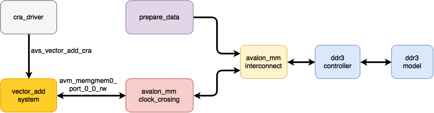
- cra_driver is a driver for configuring the kernel.
- vector_add_system is the kernel that we simulate ( DUT ).
- avalon_mm_clock_crossing - transfer of data from the frequency of the kernel (140 MHz) to the frequency of reading from the controller (100 MHz) and back.
- prepare_data are simple tasks that write data to buffers X and Y before starting the simulation.
- avalon_mm_interconnect - multiplexing and arbitration of two Avalon-MM interfaces.
- ddr3_contoller , ddr3_model - Altera Hard Memory Controller and DDR3 simulation models. The model and controller settings are the same as those used in the hps module .
The driver for configuring the kernel is just a sequential call to the next task with the kernel settings that we dug out thanks to SignalTap:
task cra_write( input bit [3:0] _addr, bit [63:0] _data, bit [7:0] _byteenable ); $display("%m: _addr = 0x%x, _data = 0x%x, _byteenable = 0x%x", _addr, _data, _byteenable ); @( posedge clk ); cra_addr <= _addr; cra_wr_data <= _data; cra_byteenable <= _byteenable; cra_wr_en <= 1'b0; @( posedge clk ); cra_wr_en <= 1'b1; @( posedge clk ); cra_wr_en <= 1'b0; // dummy waiting repeat (10) @( posedge clk ); endtask Hidden text
initial begin wait( ram_init_done ); wait( test_data_init_done ); cra_write( 4'h5, 64'h000F424000000000, 8'hF0 ); cra_write( 4'h5, 64'h0000000100000000, 8'hF0 ); cra_write( 4'h6, 64'h00000000000F4240, 8'h0F ); cra_write( 4'h6, 64'h0000000100000000, 8'hF0 ); cra_write( 4'h7, 64'h0000000000000001, 8'h0F ); cra_write( 4'h7, 64'h0000000100000000, 8'hF0 ); cra_write( 4'h8, 64'h0000000000000001, 8'h0F ); cra_write( 4'h8, 64'h0000000100000000, 8'hF0 ); cra_write( 4'h9, 64'h00000000000F4240, 8'h0F ); cra_write( 4'h9, 64'h0000000100000000, 8'hF0 ); cra_write( 4'hA, 64'h0000000000000001, 8'h0F ); cra_write( 4'hA, 64'h0000000000000000, 8'hF0 ); cra_write( 4'hB, 64'h0000000000000000, 8'h0F ); cra_write( 4'hB, 64'h0000000000000000, 8'hF0 ); cra_write( 4'hC, 64'h0000000020100000, 8'h0F ); cra_write( 4'hC, 64'h0000000000000000, 8'hF0 ); cra_write( 4'hD, 64'h0000000020500000, 8'h0F ); cra_write( 4'hD, 64'h0000000000000000, 8'hF0 ); cra_write( 4'hE, 64'h0000000020900000, 8'h0F ); cra_write( 4'hE, 64'h0000000000000000, 8'hF0 ); cra_write( 4'h0, 64'h0000000000000001, 8'h0F ); end For the preparation of data for which it is necessary to make a calculation, we write a similar task that will be written into memory at addresses that have been filled in in advance. (We don’t need to ask anyone (the system) to allocate addresses). For the demonstration, it is not necessary to write down 2x1000000 numbers as necessary according to the conditions of the problem - a couple of thousand is enough to see how it works. If we do not write the data, x will be read from memory ( unknown value ), since nothing was written to these cells.
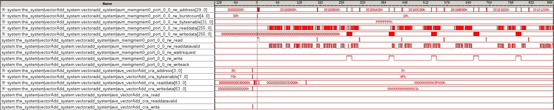
We look at the simulation result (all the numbers on the timeframes in hexadecimal form) (it is better to open the screenshots in a separate window): The start signal comes
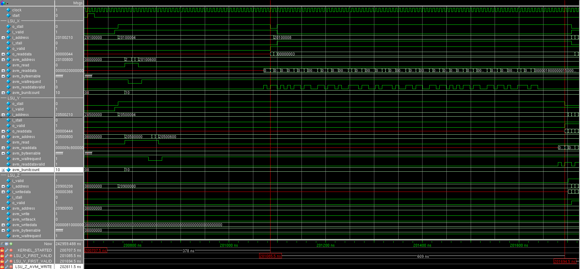
and after several cycles, both LSUs simultaneously issue a request to read data with a bursts size equal to 0x10 = 16. Interestingly, three requests are first received only from LSU_X , and then from LSU_Y : this is seen by the avm_waitrequest signal, the read request is accepted only when there is a waitrequest equals zero. Why requests do not alternate, as one would expect - this is a question to the sheduller and interconnect to global memory.
Why were there three requests?
The number of words in the FIFO in LSU is 64, and one would expect 4 read requests, but this trick was done there:
parameter READTHRESHOLD = FIFODEPTH - MAXBURSTCOUNT - 4; assign too_many_reads_pending = (reads_pending + fifo_used) >= READTHRESHOLD; // make sure there are fewer reads posted than room in the FIFO We sent 3 read requests (3 x 16 = 48 words): there is still room for 16 words, but the reading will stop until four words are spent. There will be no small bursts out of 12, because This module does not know how (and there is no special reason for this - to spend extra logic).
After some time, come to read the data (see the signal. LSU_X_avm_readdatavalid ) and shortly exposed signal LSU_X_o_valid , informs that 32-bit data in LSU_X_o_readdata ready for further processing, but we caulk: LSU_X_i_stall is set to one. The fact is that the conveyor that will add data has no data from LSU_Y . Therefore everything shuts up until LSU_Y_avm_readdatavalid comesand set LSU_Y_o_valid .
The next clock after that comes LSU_Z_i_valid , which notifies LSU_Z_i_writedata of vadidity : the addition pipeline has worked for one clock. LSU_Z waits for the accumulation of the required amount of data: this is of course 16,256-bit words and performs a write transaction. In parallel, LSU_X and LSU_Y make their read transactions as they empty their FIFOs. Note that LSU_X_i_stall and LSU_Y_i_stall are not cocked, which means that the pipeline does not shut up and each clock receives new data.
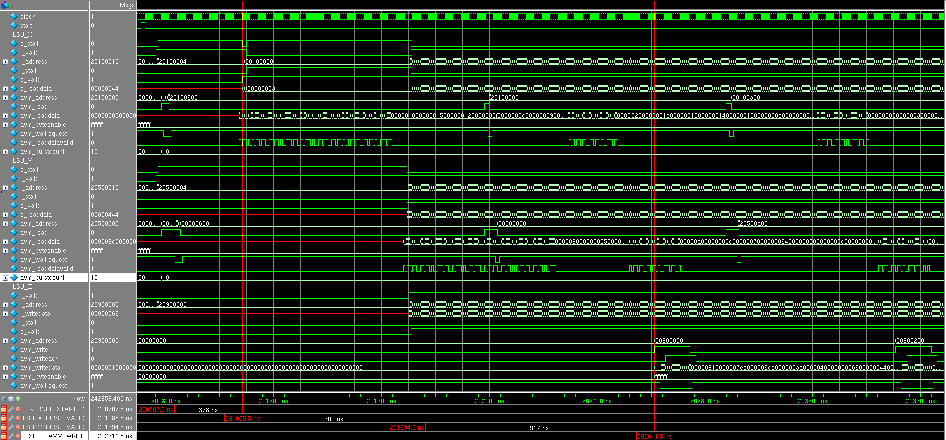
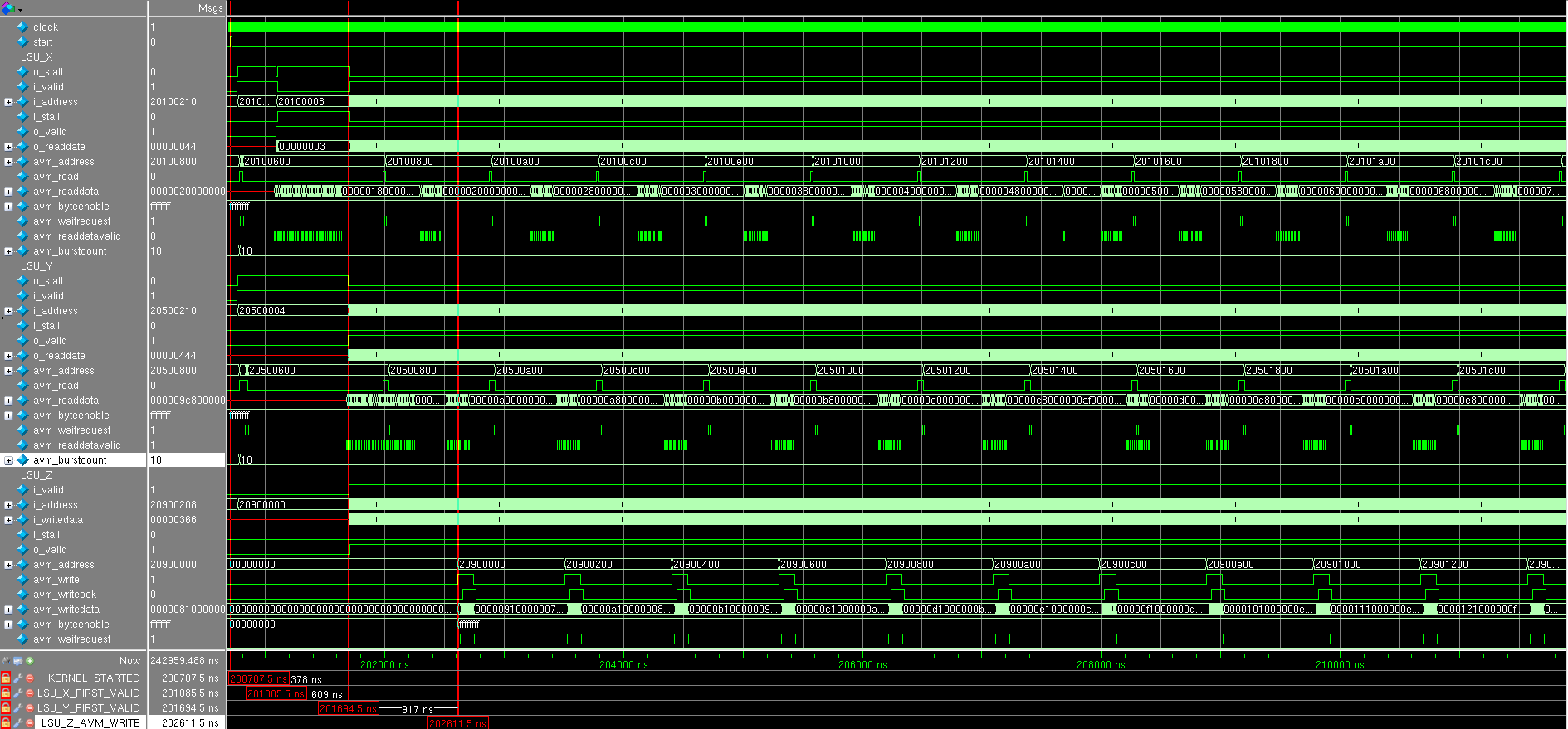
After seeing a lot of the number of transactions, it is clear that no more plugging occurs.
Conclusion :
Due to the fact that the pipeline never stops (except at the very beginning), it is clear that it works with maximum performance, and that it is the narrow link in this simple example. Since reading takes place in 256-bit words, it makes sense to organize parallel addition of eight 32-bit numbers - then the bottle is most likely to occur in memory access. Used to proc eed number of adders special meaning does not
Thanks to the simulation, we can make some changes to the RTL code (for example, the length of the bursts or the size of the caches) in order to see how this will affect the speed of the calculations and very quickly see the answer: you do not need to wait 10-15 minutes for this to rebuild the whole project with Quartus - just run the simulation in the simulator.
Of course, some architectural changes need to be made through editing the * .cl file (for example, using special directives): you can regenerate the code, and also run the simulation and see the resulting gain without assembling the entire project.
Conclusion
We have learned what the vector_add core is turning from the FPGA and how it is configured.
As you can see, many issues that would have arisen for FPGA developers (if they had written from scratch) were resolved:
- cache sizes
- architecture
- Interconnect made and interface arbitration
- automatic adjustment of the clock frequency to the resulting value
Of course, not the fact that what is done automatically is the most optimal.
Hidden text
, Quartus'a ( , ) «».
, :
, : — FPGA.
, , FPGA , Advisor ', GUI , . ( Altera).
, :
, : — FPGA.
, , FPGA , Advisor ', GUI , . ( Altera).
Low-level optimization and manual tuning is the very last step. Do you often climb into assembler after building gcc? First you need to carry out a high-level optimization in * .cl and play around with the settings of Quartus.
It is good that there is an opportunity to simulate the core: you can estimate its performance without having iron (board) on your hands.
Thanks for attention! I will be glad to questions and comments in the comments or in personal mail.
Source: https://habr.com/ru/post/269925/
All Articles