Ethernet + PCIe + FPGA = LOVE
Ethernet access is not possible without network cards (NIC). At low speeds (up to 1G), NICs are embedded in motherboards, and at high speeds (10G / 40G), the NIC is placed on a separate PCIe card. The main core of such a board is an integrated chip (ASIC), which is engaged in receiving / sending packets at the lowest level. For most tasks, the capabilities of this chip are more than enough.
What to do if there are not enough network card capabilities? Or does the task require as close as possible access to a low level? Then boards with reprogrammable logic - FPGA (FPGA) come onto the scene.
')
What tasks on them decide what is being placed, as well as the most interesting representatives you will see under the cut!
Carefully , there will be pictures!
Plan:
FPGA Applications
DPI, filtering and firewall
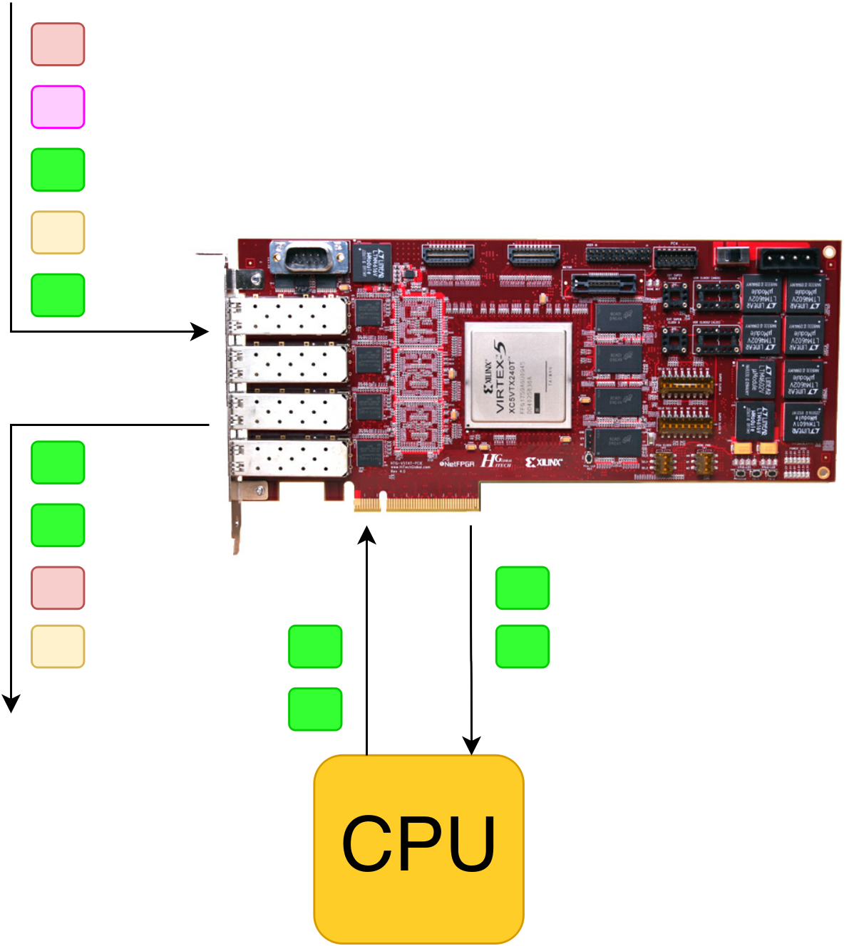
A server with such a board can get into a “gap” and monitor all packets passing through it. Intellectual DPI is implemented on the basis of the processor, and packet forwarding and simple filtering (for example, many 5-tuple rules) are implemented on the basis of the FPGA.
How can I do that:
- The streams that we trust, or the decision on them is already in the table for FPGA, pass through the chip with a slight delay, the rest are copied to the CPU and processing is done there.
- FPGA can remove some of the load from the CPU and look for suspicious signatures in itself, for example, using the Bloom algorithm . This algorithm has the probability of a false positive response, so if there was a line in the package that Bloom responded to, then such a package is copied to the CPU for additional analysis.
- The processor processes only the traffic that is interesting - FPGA selects packets according to specified criteria (for example, HTTP requests or SIP traffic) and copies them to the CPU, everything else (torrents, video, etc.) pass through FPGA without significant delay.
All these three options can be combined in different variations. The FPGA can also do some other dirty work, for example, act as a shaper / polisher, or collect statistics on streams.
In the illustration above, green packets are processed on the CPU, burgundy and yellow went through filters in the FPGA, and pink packets were dropped (also in the FPGA).
Traffic Analysis and Capture
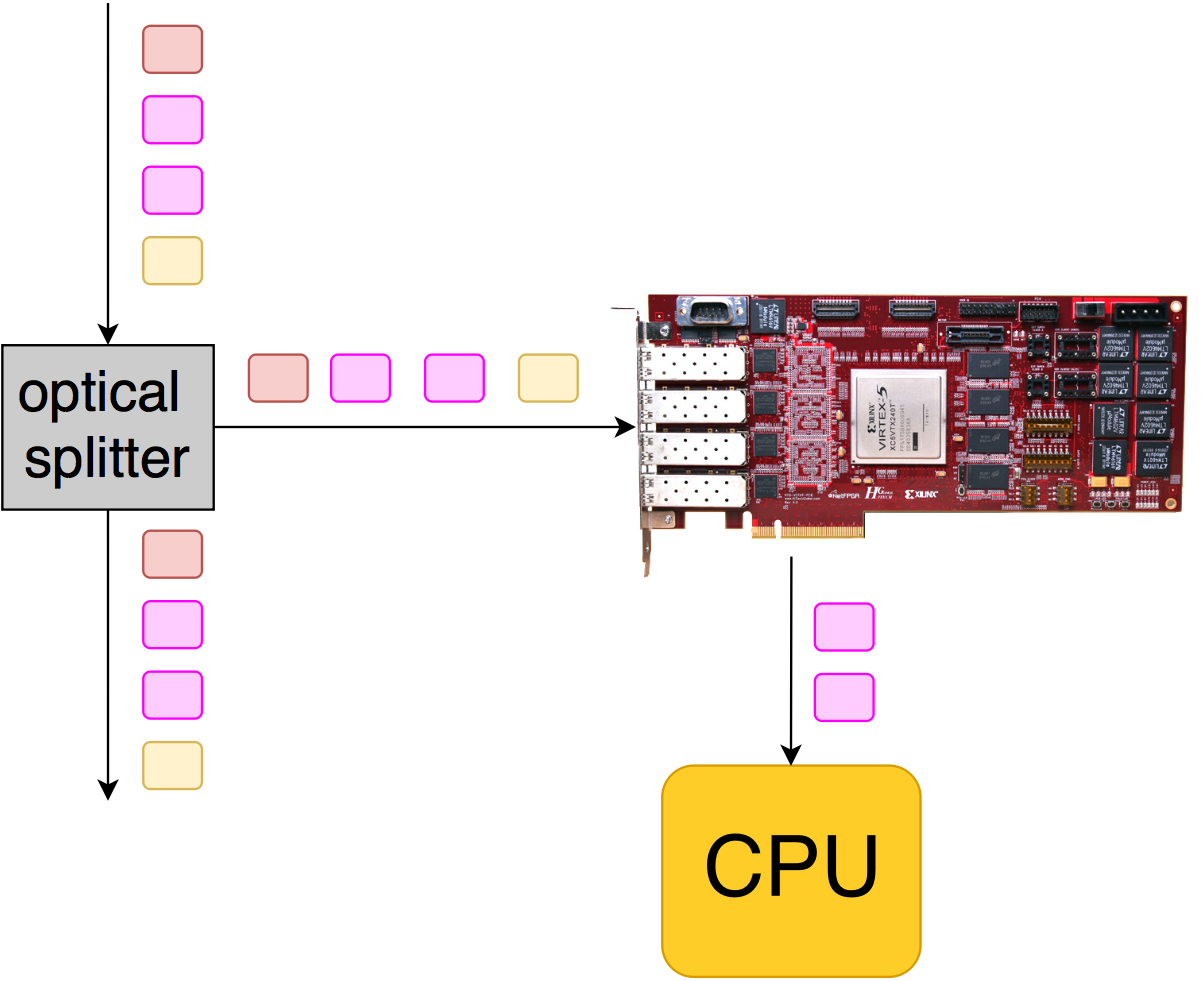
Sometimes these cards are used for capturing traffic and further post-processing on the CPU (write to pcap, delay analysis, etc.). In this case, the splitter is inserted into the links (or traffic is taken from the port mirror). It turns out non-intrusive connection, similar to how we did in the project of monitoring RTP flows .
Here from FPGA is required:
- Filtering by fields (like 5-tuple): to select only the traffic that is interesting.
- Synchronization via PTP, for hardware timestamping of packets: the time when the packet arrived is snapped up, and this label is placed at the end of the packet. Then on the CPU you can count, for example, the response time to the request.
- Slicing is cutting off only the required piece of data (most often it is the first N bytes from the packet - in order to copy only the headers, because very often the data is not very interesting,).
- Packet buffering:
- if the CPU does not have time to write in case of some bursts, then you can smooth it out by placing the packets in external memory for a couple of gigabytes
- if we want to ensure that packets are recorded for a short time (for example, after triggering), it is most often applicable for high speeds (40G / 100G).
- Spreading packets in queues and CPU cores.
Having access to the lowest level (well, almost), you can support any protocol or tunneling, and not wait for Intel to do this in their cards.
In the above illustration, the FPGA accepts all packets after the traffic is branched out, but only those that interest us (rosy) are copied to the CPU.
Network card
Cards with FPGA can be used as a normal NIC, but there is not much point in this:
- At the moment, at all Ethernet speeds (up to 100G inclusive) there are network cards based on ASICs. For the price they will be cheaper than solutions on FPGA.
- If you write the card yourself, then for more or less serious performance, you need to wrap a huge number of buns (RSS, LSO, LRO) in such a card.
Meaning appears only when it is necessary to provide a unique chip, which will never be on Intel's chip. For example, hardware encryption according to GOST or Grasshopper .
Network accelerator
Load reduction with CPU
When high speeds appear, the processor does not have time to do everything: I want to remove some of the tasks from it. For example, what happens when you copy a large amount of data over a network?
The processor should:
- take some piece of data
- put in TCP, split into several packets, according to MTU
- substitute header (MAC / IP-addresses)
- calculate cheksummy IP and TCP (although most NIC already take on it)
- pass the handle to the NIC
It is also necessary:
- follow the answers
- resend packets if the packet is lost
- reduce / increase tcp-window and so on
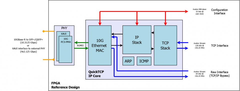
The TCP stack can be implemented on the FPGA: the CPU only needs to provide a pointer to the raw data and the recipient's IP + port, and the piece of hardware will do all the low-level work (setting up the connection, re-sending, etc.).
There are ready-made IP-cores that do all this: for example, implementations of TCP and UDP stacks from the company PLDA .
They have standard interfaces (Avalon or AXI), which makes them easy to connect to other IP cores.
Speed up response
There is a class of tasks where money is brought not by processors, but by the speed of reaction. Of course, I'm about High Frequency Trading . You can read about the role of FPGA in HFT in this article.
The PLDA website provides a video and an example of how this is done. Using hardware TCP and UDP cores allows you to reduce letensy on purchases / sales.
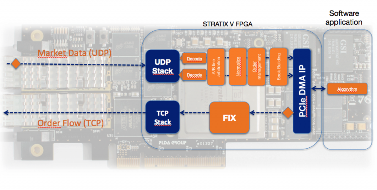
Hidden text
I apologize for the red underscores - the picture was taken from the PLDA site, and they have it in the original ...
There are special IP cores that decode data from the markets and are ready for pairing with hardware TCP and UDP stacks.
Of course, the use of standard kernels or approaches will not give a competitive advantage: exclusive solutions are being developed, since "They want even less delay . "
Measuring equipment
Network emulators
It often happens that you need to check the engineering solution in the laboratory, because in combat it can be very expensive.
Recently there was an article from CROC, about optimizing traffic in the North and a large RTT. To check the quality of services in real conditions, you first need to create these conditions in your laboratory. For this, you can use the usual Linux machine, but there are special pieces of hardware that are engaged in network emulation.
Most often it is necessary to be able to set parameters such as delay / jitter, packet loss (error). We cannot do without hardware support (read, FPGA), but we also need a smart processor to emulate various protocols (user sessions). In order not to develop hardware from scratch, you can take the server and insert a PCIe card with FPGA.
Acceleration Calculations
Such cards can also be used to speed up some calculations or simulations, for example, for biology or chemistry. An example of such a simulation told Algeronflowers in this article. In this case, the Ethernet ports may not be necessary, but on the other hand they can be useful if you want to make a farm from the boards: transfer input or output data for the calculation via Ethernet.
Opencl

Sometimes there is no need to squeeze out all the juice from the iron: very often time-to-market is important. Many developers refuse to use FPGA, because they are frightened by the low-level optimization to the cycles (plus you need to know the new language (s) and tool). I would like to write code at the “high” level, and the compiler will already decompose everything into triggers / memory blocks. One such option is OpenCL . Altera and Xilinx support.
OpenCL on FPGA is the topic of a separate article (and not one). I recommend to familiarize with the presentation from Alter about the technology review and the route of development for FPGA.
Highload
On the Internet you can find a lot of news, that the giants are looking at the FPGA for processing big data in data centers.
So, there was a note that Microsoft used FPGA to speed up the search engine Bing. Technical details can be found in A Reconfigurable Fabric for Accelerating Large-Scale Datacenter Services .
Unfortunately, there is no good technical article in Russian about this, although the topic is very interesting. Can olgakuznet_ms or her colleagues fix this flaw?
I hope that the release of CPU + FPGA chips will spur developers of highly loaded systems to transfer part of the calculations to FPGA. Yes, development under FPGA is “more difficult” than under CPU, but on specific tasks it can give a remarkable result.
Development / debugging of IP-cores and software
Such cards can still be used by ASIC / FPGA developers to verify their IP cores, which can then be run on completely different hardware.
It often happens that the software is written at the same time as the piece of hardware is being developed / manufactured, and it is already necessary to debug the software somewhere. In this context, software is like FPGA + firmware, various drivers and user programs. In the 100G project of the analyzer and balancer , problems arose that we never solved:
- FPGA tuning (CSR: status control registers) must occur via PCIe
- for linux'a FPGA with a bunch of interfaces should look like a network card: you need to write the driver (s), and transfer packages from / to the host
Of course, there were other tasks in parallel (such as the generation / filtering of 100G traffic), but they were easily solved in the simulator, but these two tasks in the simulator are not particularly chasing. What have we done? It turned out that we have a devbord from Altera. Despite the fact that there is a completely different chip, another PCIe, etc., we debugged a bunch of FPGA + drivers on it, and when the production department handed us the board for b100, then after raising the iron, the whole bunch worked without problems.
General scheme
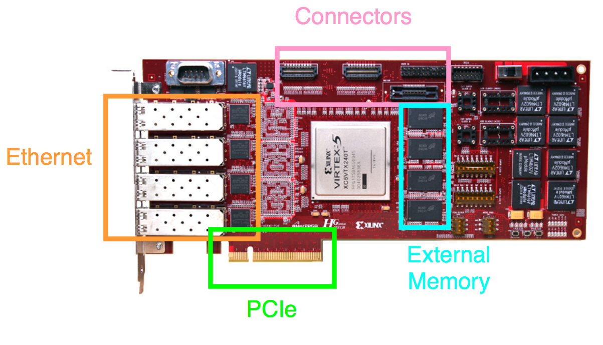
Before reviewing the cards, consider the general scheme of such PCIe cards.
Ethernet
The boards are equipped with standard Ethernet connectors:
- SFP - 1G
- SFP + - 10G
- QSFP - 40G
- CFP / CFP2 / CFP4 - 100G
The most common combinations are:
- 4 x SFP / SFP +
- 2 x QSFP
- 1 x CFP
About what is happening at a low level and how the connection to 10G to integrated circuits takes place can be found, for example, here .
PCIe
A standard connector that can be plugged into a computer with an ordinary motherboard. Currently, top FPGAs support Gen3 x8 hardware IP cores, but this bandwidth (~ 63 Gbps) is not enough for all tasks. On some boards, there is a PCIe switch that combines 2 Gen3 x8 channels into one Gen3 x16.
On future chips, Altera and Xilinx announce hardware support for Gen3 x16, and even Gen4.
Connectors
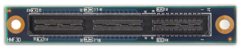
Sometimes place the connector (s) for connecting expansion cards, but there is no single de facto standard (such as USB). The most common are VITA ( FMC ) and HSMC .
Avago MiniPod
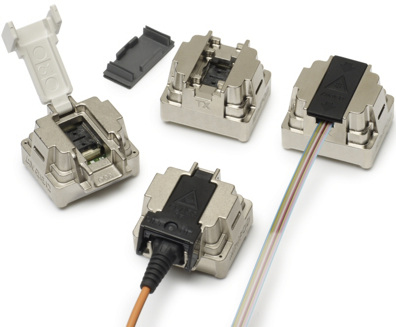
The above connectors have a slight drawback - they are metallic and at high frequencies / long distances the attenuation can be significant.
In response to this problem, Avago developed Avago Minipod : optical transceivers. They are ready to transfer 12 Lane 10-12.5GBd. The size of the connector is comparable to the coin. With this connector, you can connect not only nearby boards, but also make connections in supercomputers or in racks between servers.
When our colleagues showed the MiniPod demo on such a board , they said that no additional IP cores or Verilog-code should be inserted - these modules are simply connected to the I / O of the FPGA transceivers, and everything works.
External memory
There are not so many memories in FPGAs - in the top 50-100 Mbit chips. To handle big data, external memory is connected to the chip.
There are two types of memory:
The selection takes into account such parameters as price, volume, delays for sequential / random reading, throughput, power consumption, availability of memory controllers, easy wiring / replacement, and so on.
Altera has an External Memory Interface Handbook , which, as it is not difficult to guess, is dedicated to external memory. The interested reader in the chapter Selecting Your Memory will find comparison tables for various types of memory and tips for choosing. The guide itself is available here (carefully, the file is large).
If you look at the use of memory in communication networks, the tips are something like this:
- DRAM is used to create large buffers (for packets).
- SRAM:
- decision tables / structures where to send the packet
- queue management structures
- packet statistics calculation (RMON, etc.)
- hybrid approach is possible - DRAM is used to store the payload of the packet, and only the header is placed in SRAM
If you open the presentation of Anatomy of Internet Routers from Cisco, you can see that they use RLDRAM as DRAM in some routers.
HMC
HMC (Hybrid Memory Cube) is a new type of RAM memory, which in some applications can displace DDR / QDR memory: they promise a significant acceleration of bandwidth and lower power consumption. On Habré you can find news: one and two . In the comments to them you can find fears that this is still far away and so on.
I assure you that everything is not so bad. So, six months (!) Ago, our colleagues from EBV showed a working demoboard of four Stratix V (on the sides) and HMC (in the center).
Commercial samples (for mass production) are expected to be available in 2015.
Review of PCIe cards
The review is probably too loud a word - I will try to show the most interesting representatives from different companies. There will be no comparison or unpacking tables. In fact, there will not be much variety between the boards, they all fit into the “pattern” that was described earlier. I am sure that you can find about five or seven companies that produce such cards, and about a dozen more boards.
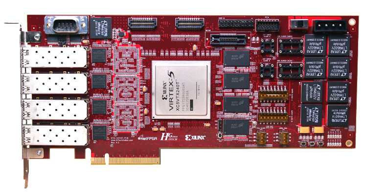
NetFPGA 10G
Hidden text
FPGA:
10-Gigabit Ethernet networking ports
Quad Data Rate Static Random Access Memory (QDRII SRAM)
Reduced Latency Random Access Memory (RLDRAM II)
- Xilinx Virtex-5 TX240T
- 240K logic cells
- 11,664 Kbit block RAM
10-Gigabit Ethernet networking ports
- 4 SFP + connectors
Quad Data Rate Static Random Access Memory (QDRII SRAM)
- 300MHz Quad data rate (1.2 Giga transactions every second), synchronous with the logic
- Three parallel banks of 72 MBit QDRII + memories
- Total capacity: 27 MBytes
- Cypress: CY7C1515KV18
Reduced Latency Random Access Memory (RLDRAM II)
- Four x36 RLDRAMII on-board device
- 400MHz clock (800MT / s)
- 115.2 Gbps peak memory throughput
- Total Capacity: 288MByte
- Micron: MT49H16M36HT-25
This is not the top card, but I could not tell about it:
- NetFPGA boards are positioned as “open platforms for research”: they are used throughout the world (in more than 150 institutions). Students / researchers can do various labs / projects for them.
- the project is positioned as opensource: there is an organization of the same name on github. On the githaba in the private repository there are various reference designs (network card, switch, router, etc.), which are written in Verilog and distributed under the LGPL. They will be available after a simple registration .
Advanced IO V5031
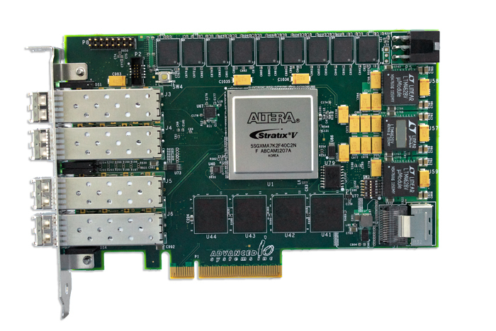
Hidden text
- Altera Stratix V
- Quad 10 Gigabit Ethernet SFP + optical ports
- 2 banks of 1GB to 8GB 72-bit 1066MHz DDR3 SDRAM
- 4 banks of 36Mbit to 144Mbit 18-bit 350MHz QDRII + SRAM
- x8 PCI Express Gen 3
- PPS Interface for time synchronization with microsecond resolution
This board has a twin brother: captureXG 1000 , but it is already positioned as a card for recording data streams:
Hidden text
- Time Synchronization: IRIG-A, B and G time synchronization
- Filters: 128 programmable 5-tuple filters (IPv4, TCP, UDP, ICMP, ARP)
- Packet Capture: PCAP Next Generation format or raw data format
In fact, the card that was shown above, wrote the firmware for the FPGA, as well as the driver. And it already turns out another product that is ready to work out of the box. I wonder what the difference in money between the two products.
Napatech NT40E3-4-PTP
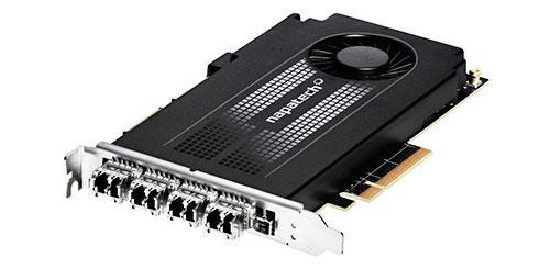
Another card for recording and analyzing traffic:
Hidden text
Alas, it was not possible to squeeze more technical details from the marketing brochure.
- FPGA: Xilinx Virtex-7
- Quad 10 Gigabit Ethernet SFP + optical ports
- 4 GB DDR3
- PCIe x8 Gen 3
Alas, it was not possible to squeeze more technical details from the marketing brochure.
In this case, it looks very pretty. Fundamentally, this card is not very different from the others, but Napatech considers it as a finished product and screwed in a bunch of features that are implemented on the FPGA:
Hidden text
- Hardware Time Stamp
- Full line-rate packet capture
- Frame buffering
- Frame and protocol information
- Time stamp injection
- Buffer size configuration
- Onboard IEEE 1588-2008 (PTP v2) support
- Inter-Frame Gap Control
- Frame Classification
- HW Time Synchronization
- Extended RMON1 port statistics
- Advanced statistics
- Synchronized statistics delivery
- Flow identification based on hash keys
- Dynamic hash key selection
- Frame and flow filtering
- Deduplication
- Slicing
- Intelligent multi-CPU distribution
- Cache pre-fetch optimization
- Coloring
- IP fragment handling
- Checksum verification
- Checksum generation
- GTP tunneling support
- IP-in-IP tunneling support
- Filtering inside tunnels
- Slicing inside tunnels
All this can be done on other cards. Just need to spend time on it.
COMBO-80G
Hidden text
- Virtex-7 FPGA chip manufactured by Xilinx company
- 2 × QSFP + cage multi / single mode, CWDM or copper
- 4 × 10G to 40G fanout modules for 10G Ethernet technology
- PCI Express 3.0 x8, throughput up to 50Gb / s to software
- 2 × 72Mbits QDRII + SRAM memory
- 2 × 1152Mbits RLDRAM III memory
- 2 × 4GB DDR3 memory
- External PPS (Pulse per second) synchronization
- Unique on-the-fly FPGA boot system (no need for host computer reboot)
Nallatech 385A and Nallatech 385C

Hidden text
385A:
385C:
General:
- Arria 10 1150 GX FPGA with up to 1.5 TFlops
- Network Enabled with (2) QSFP 10/40 GbE Support
385C:
- Altera Arria 10 GT FPGA with up to 1.5 TFlops
- Network Enabled with (2) QSFP28 100 GbE support
General:
- Low Profile PCIe form factor
- 8 GB DDR3 on-card memory
- PCIe Gen3 x8 Host Interface
- OpenCL tool flow
As you can see, these are two twin brothers: the 385A has a more budget FPGA (GX) with 17.4 Gbps transceivers, which is enough for 10 / 40G, while the 385C already uses the Arria 10 GT, since need 28 Gpbs transceivers to support 100G, which come in 4x25G performance.
I note that Nallatech provides OpenCL BSP for these cards.
HiTech Global 100G NIC
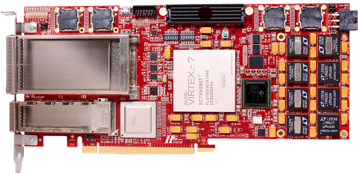
Hidden text
- x1 Xilinx Virtex-7 H580T
- x16 PCI Express Gen3 (16x8Gbps)
- x1 CFP2 (4x25Gbps)
- x1 CFP4 (4x25Gbps)
- x1 Cypress QDR IV SRAM
- x2 DDR3 SODIMMs (with support up to 16GB)
- x4 Avago MiniPod (24 Tx and 24 Rx) for board-to-board high-speed communications
- x1 FMC with 8 GTH transceivers and 34 LVDS pairs (LA0-LA33)
Here we are seeing both the FMC connector for connecting other boards, and the Avago MiniPod, which we talked about earlier.
Bonus:
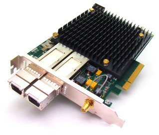
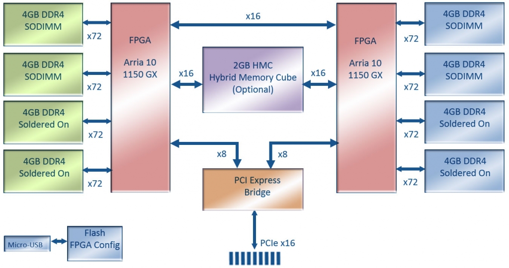
Nallatech 510T
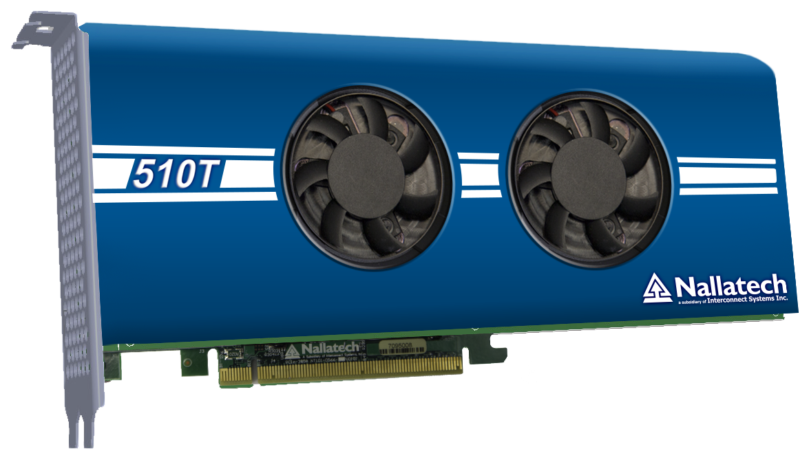
There is no Ethernet in this card, but this is a real bomb .
Hidden text
- GPU Form Factor Card with (2) Arria 10 10A1150GX FPGAs
- Dual Slot Standard Configuration
- Single Slot width possible, if user design fits within ~ 100W power footprint
- PCIe Gen3 x 16 Host Interface
- 290 GBytes / s Peak Aggregate Memory Bandwidth:
- 85GB / s Peak DDR4 Memory Bandwidth Per FPGA (4 Banks per FPGA)
- 30GB / s Write + 30GB / s Read Peak HMC Bandwidth per FPGA
Here and two fatty top-end chips, which are riveted on 20-nm technology, and DDR4, and HMC. Performance promises up to 3 TFlops!
Judging by the render, it’s still far from a real piece of iron, but it is felt that it will be gold (for the price), but it will take its niche: it is positioned as a coprocessor for data centers. They promise support for OpenCL, which means that no one will be babysitting to the beat with this board: they will drive ready-made algorithms and burn watts. Who knows, maybe on this board Youtube, Facebook, VK will convert the video, replacing dozens of servers? Or maybe special effects for a new Avatar will be rendered on such farms?
Conclusion
Having looked at all this variety of boards, my colleagues and I thought: why don't we also make such a card?
According to the complexity of the printed circuit board, it will not be more complicated than the B100 , we seem to be able to write software for FPGA and Linux, and there is a demand for certain companies and departments for such hardware.
My colleagues and I argued a little about which card to make, and we are interested in what you think about this.
Thanks for attention! Ready to answer questions in the comments or in PM.
Source: https://habr.com/ru/post/267183/
All Articles