Who is better or Walsh vs. Fourier
Despite the development of science and technology, the compression of information still remains one of the urgent problems, where video compression algorithms occupy a special place. This publication will focus on the compression of static color images by JPEG-like algorithms.
First I want to thank the author of the articles "JPEG decoding for dummies" and "Inventing JPEG" , which greatly helped me in my work on writing this publication. When I took up the study of lossy image compression algorithms, then in part of the JPEG algorithm I was constantly tormented by the question: “Why is the role of the basic transformation in the JPEG algorithm specifically for the special case of the Fourier transform?”. Here the author gives an answer to this question, but I decided to approach it not from the point of view of a theory, mathematical models or software implementation, but from the point of view of circuit engineering.
The JPEG image compression algorithm is a digital signal processing algorithm, which, in hardware, is usually implemented either on digital signal processors or on programmable logic integrated circuits. In my case, the choice for the operation of a digital signal processor would mean coming to what I was trying to get away from - to a software implementation, so it was decided to stop at a programmable logic.
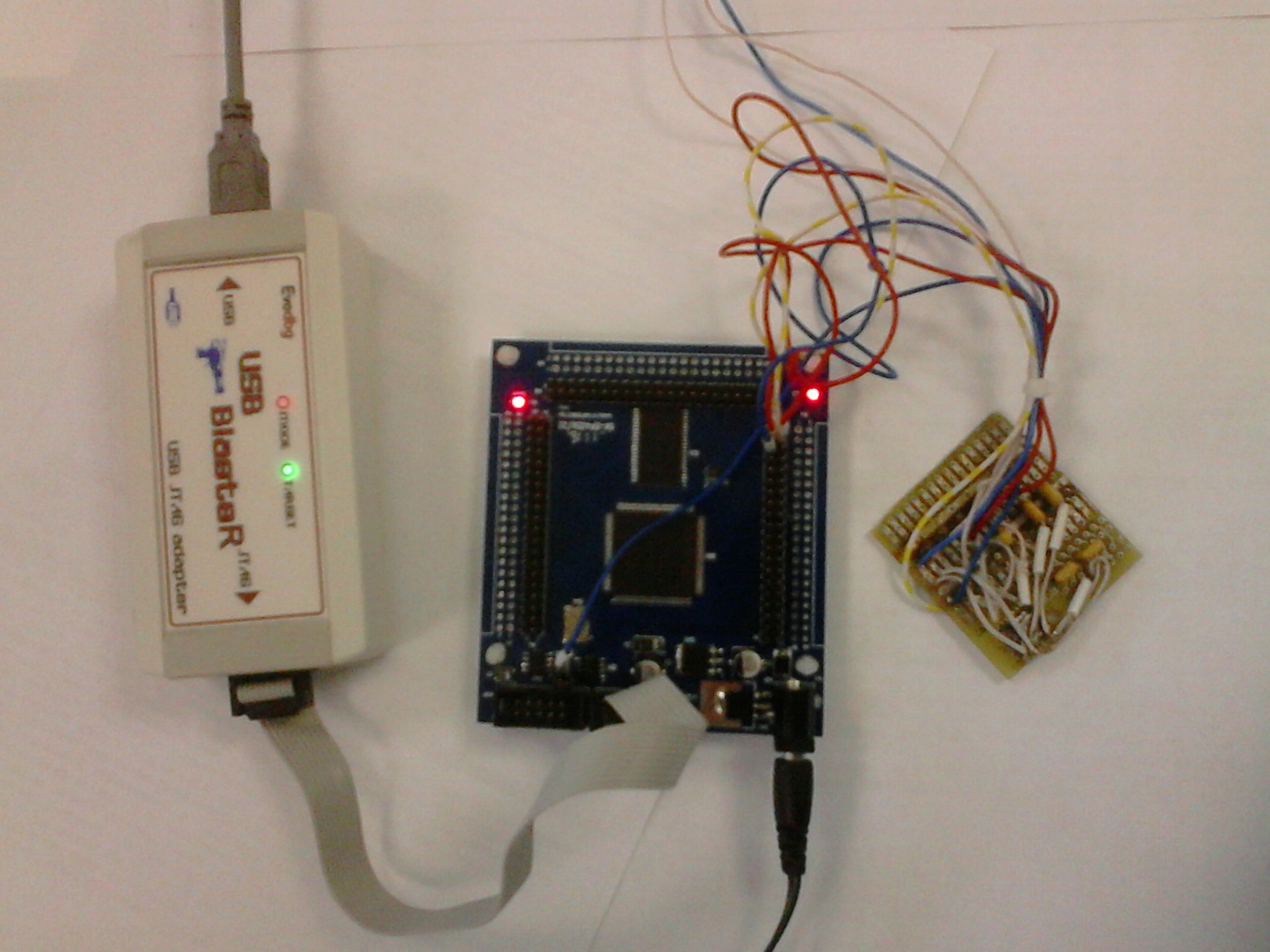
In one of the online stores, I purchased a fairly simple debug board , which contains Altera FPGA Cyclone 4 -EP4CE6E22 FPGA and SRAM 512Kx8 memory. Since the FPGA was from Altera, it was decided to use the Quartus II Web Edition environment for development. Development of individual functional blocks of the hardware codec was carried out in the Verilog language , and assembly into a single scheme was carried out in the graphical editor of the Quartus II Web Edition environment.
')
To communicate with a personal computer (receiving commands, receiving / transmitting the processed data), in Verilog I wrote a simple asynchronous UART transceiver. To connect to the COM-port ( RS-232 ) of the computer, based on the MAX3232WE chip and from what was at hand, hastily, the level converter was soldered. In the end, here's what happened:
For sending commands from a personal computer, as well as receiving and transmitting data, a trial version of the ADVANCED SERIAL PORT MONITOR program was used, which allows you to create not only individual parcels of data bytes, but also generate data streams from the file contents, and also record received data streams to a file, which allowed to send and receive files. I do not use and control any protocols and checksums for receiving / transmitting data via UART (I was simply too lazy to envisage and implement all this); during the communication for receiving / transmitting, I used what is called “raw data”.
All arithmetic operations associated with fractional numbers in the codec are carried out in a fixed-point format, addition and subtraction operations are carried out in an additional code , in principle this is understandable. How the bit depth of the processed data was determined will be described below.
The compression operation is performed on the source images presented in the .bmp format with a color depth of 24 bits per pixel (8 bits for each of the color components).
The memory available on the debug board was organized as follows: addresses from 00000h to 3FFFFh (in hexadecimal numbering system ) were allocated for storing source data (picture in .bmp format for compression, or coded data for unpacking), totaling 256 KB, the remaining 256 KB space for recording received, as a result of data compression or decompression, these are addresses from 40000h to 7FFFFh. I think it is obvious that the maximum size of compressible images is limited by the amount allocated for data storage, memory.
The algorithm of the device operation is as follows: immediately after the power supply, the codec waits for a data stream via the UART, any data received, while the data is interpreted as an initial file for processing, if the pause between bytes is 10 ms, then this is interpreted as the end of the file and following the pause Bytes received by the UART are perceived by the device as a command. Commands are specific byte values. For example, after receiving a file after 10 ms, received by the UART codec, the value of byte AAh is interpreted by the device as a command that sends data from the memory chip to the computer via the UART, starting at address 40000h and ending with the value of the address at which the processed data was written i.e. The results of compression / decompression are transmitted to the computer. The value of EEh is interpreted as a command for compressing / decompressing an image, and also for debugging I provided a number of other commands.
As for the structure of the file with the compressed image, then I decided not to bother, and, in contrast to the JPEG algorithm, the algorithm I implement is rather narrowly targeted and not designed for all occasions, therefore, the resulting data as a result of compression the stream is written to the allocated memory area. The only thing that needs to be noted here is that in order not to implement the header generator for the .bmp file (it was also lazy), during compression, it is simply completely rewritten to the initial (from the address 40000h) memory area reserved for the final data, and then, starting with the offset from which pixel data is stored in the source .bmp file, compressed data is written. This offset is stored in the header of the .bmp file at 0Ah relative to its beginning, and is typically 36h. When unpacking, the same operation is performed accordingly.
So, image compression of JPEG-like algorithms is performed in the following sequence:
Unpacking is in reverse order.
Of all the steps listed above, in the codec, I did not implement sub-sampling, as I considered it superfluous (maybe I’m wrong).
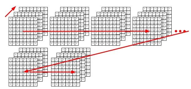
Based on the above sequence of actions, I developed the following functional codec scheme:
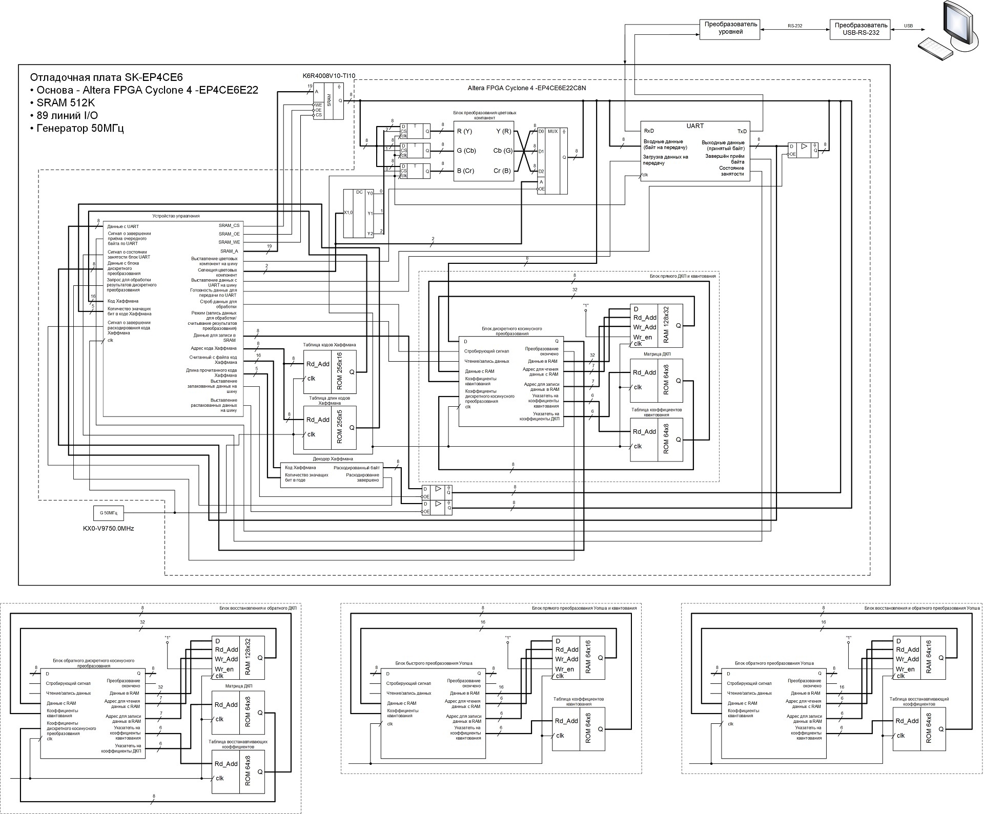
The codec operation process is controlled by a control device, which is a finite state machine, here the coding / decoding of run lengths is performed, as well as the generation of final data from Huffman codes during compression and the formation of the Huffman codes themselves from data received from the SRAM memory during unpacking. The control unit also generates control signals for other operating units.
Under the main circuit, there are diagrams of operating units, changing them in the main circuit, I changed the modes of operation of the device. There was an attempt to collect everything into a single device and set the modes of operation of the codec, as well as methods of basic transformation using the commands on the UART, but the logical capacity of the FPGA was not enough. Therefore, the operation modes of the device are changed by changing the corresponding operational blocks and the task of certain parameters in the control device (including the size of the compressible / unpacked image), after which the modified project is compiled and stitched into the FPGA.
On the Internet you can find a lot of different information on the transformation of color spaces, so I will immediately begin with a description of the hardware implementation.
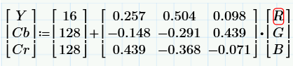
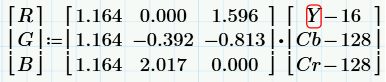
The color space conversion block is a combinational logic, due to which the color components are transformed in one generator cycle. The conversion of the RGB color space to YCbCr is performed by the following formulas:
The calculation begins with the control device setting the starting address of the SRAM memory chip to the starting address from which the pixel data is stored in the .bmp file, as mentioned above, the starting address is 36h. The .bmp files at this address store the value of the blue color component of the lowest right pixel of the image. At address 37h, the value of the green color component, then red, then the blue component of the next pixel in the bottom line of the image again, etc. As you can see from the functional diagram, there is a register for each color component in the scheme. After loading from memory all three color components into their registers, from the next clock of the generator recording of the results of calculations is carried out in memory. So, the monochromatic red component “Cr” is recorded at the address of the blue component “B”, the monochromatic blue component “Cb” is recorded at the address of the green component “G”, and the component “Y” is recorded at the address “R”. As a result of this step, the same image in YCbCr format will appear in place of the original image in the SRAM memory in RGB format.
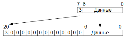
For the hardware implementation of calculations of the brightness and monochromatic components, all fractional coefficients from the formulas were presented in the form of sixteen-bit words in a fixed-point format, where the upper eight bits contain an integer part, respectively, the lower eight bits have a fractional part. For example, the coefficient 0.257 in binary representation with a fixed point looks like this: 0000000001000001 or in hexadecimal form 0041h. The limited number of digits reduces the accuracy, so if the fractional binary number 0000000001000001 is converted to decimal form, we get: 2 ^ (- 2) + 2 ^ (- 8) = 0.25 + 0.00390625 = 0.25390625. As you can see, the result differs from the value of 0.257 and in order to improve the accuracy of the presentation, the number of digits allocated for the fractional part should be increased. But I decided to limit, as mentioned above, to eight digits.
So, in the first stage of the conversion, the eight-bit values of the RGB color components are converted to sixteen-bit in a fixed-point format by adding eight low-order bits filled with zero bits:
At the second stage, multiplication, addition and / or subtraction operations are carried out. As a result, thirty-two-bit data is obtained, where the sixteen senior digits contain an integral part, and the sixteen low-order ones contain fractional part.
In the third stage, eight-bit data is formed from the thirty-two-digit words obtained by selecting eight bits immediately before the comma (if the lowest-order bit is 0 and the oldest is 31, then these are bits 23 to 16):

At the fourth stage, to the obtained eight-bit words, in accordance with the above-presented formulas, offsets are added (for component Y - 16, for components Cb, Cr - 128).
Conversion from YCbCr to RGB is carried out according to the following formulas:
Here there is such a feature that the results of calculations, in some cases, can acquire values greater than 255, which goes beyond one byte, or negative values, respectively, such situations need to be monitored.
So, if an overflow occurs, the value of the resulting color component should be equal to 255; for this, we simply perform a bitwise logical OR operation of the result with an overflow bit. And if the sign digit of the result is equal to one (i.e., the value is less than zero), then the value of the final color component should be 0, for this, we perform a bitwise logical operation “AND” of the result with the inverted value of the sign bit.
So, at the first stage of converting the YCbCr color space into RGB, read from the SRAM memory chip, we translate the eight-bit values of the luminance and monochromatic components into an additional ten-bit code, by adding two high-order zero bits (the sign bit and the overflow flag). As a result, we get ten-bit words. Further, in accordance with the formulas, we subtract from these values of the offset (or add the negative values of the offsets presented in the ten-bit additional code). Then, we translate the result obtained from the additional code into the straight line, preserving the values of the highest (sign) bit. The remaining nine-bit words will be converted to eighteen-bit with a fixed point path, attributing the lower nine bits with zero bits:
Fractional coefficients appearing in the formulas are also represented in the form of an eighteen-bit code with a fixed point, where 9 bits are allocated for the integral and fractional parts. As a result of multiplication operations, we get thirty-six-bit values of products, in which 18 high-order bits - the whole part, 18 low-order bits - fractional. Then we calculate the sign of the product by performing a logical operation “addition modulo 2”, a previously stored sign bit with a sign before the coefficient in the formula (if “-”, then “1”, if “+”, then “0”).
It is also necessary to determine whether the result of the product is zero, if the result of multiplication is zero, then 0 must be written in the sign bit, regardless of the signs before the coefficients and the signs of the results obtained as a result of the offset of the components read from the memory. To do this, apply the reduction operator (| product [35: 0]) to the product, which determines whether all the bits are equal to zero as a result of multiplication (if so, the result of the operation of this operator will be zero), and then perform a logical AND operation the result obtained with the result of the operation "addition modulo 2" sign digits.
After all this, we translate the results of the multiplication into an additional thirty-seven-digit code, where the sign is stored in the most significant digit, and perform addition operations. After the addition operations, obtained in the additional code, we translate the results into a direct code, and select eight bits immediately before the comma (if the number of the least significant bit 0 and the most significant one is 36, then these are bits 25 to 18). Next, we check if there was an overflow; for this, as mentioned above, we perform a bitwise logical “OR” operation of eight bits allocated with an overflow sign, which is stored in the 26th digit. And yet, we check whether a negative result is obtained, for which we perform a bitwise logical operation of the “And” of an inverted sign bit with the same eight bits:
The resulting, calculated by three formulas, and the converted eight-bit values are the values of the RGB color components.
I decided to test the device using a 256 by 256 pixel photo of Lena Soderberg:
Everyone working in image processing works with this photo, and I decided not to be an exception.
So, as a result of the conversion of the original photo loaded on the UART to the SRAM memory of the debug board, from the RGB color space to the YCbCr space, the following image was obtained:

The picture below shows the original photo on the right, the photo on the left is the result of the inverse transformation from the YCbCr space into the RGB color space as described above:
When comparing the original and transformed photographs, you can see that the original photograph is brighter than the processed one, this is due to the loss of data that occurred during rounding (“garbage” of the fractional part), as well as loss of accuracy, when representing fractional coefficients in binary form.
Information about what a discrete cosine transform (hereinafter referred to as DCT), on the Internet is present in sufficient quantity, so I’ll dwell briefly on the theory.
As mentioned in this publication, the essence of any basic transformation is reduced to multiplying the transformation matrix by the input data matrix, after which the result is again multiplied by the transposed matrix of the same transformation. In the case of a discrete cosine transform, the coefficients of the transform matrix are calculated according to the following rule:
Where:
N is the dimension of the matrix;
i, j - indices of matrix elements.
In our case, N = 8, i.e. the original image is divided into blocks of 8 by 8 pixels, while the values of the indices i and j vary in the range from 0 to 7.
As a result of applying this rule for N = 8, we obtain the following transformation matrix:
In order not to carry out calculations with fractional numbers, we multiply each element of the matrix by 8√8, and round the obtained values of the elements of the matrix to integers, with the result that we get the matrix T:
In this case, it will be necessary to divide the result of matrix multiplication, as in the case of direct discrete cosine transform when encoding, and in the case of the opposite when decoding, divided by 512. Given that 512 = 2 ^ (9), then division is done by shifting the dividend to the right by 9 positions.
As a result of the direct discrete cosine transform, a matrix is obtained of the so-called DCT coefficients, in which the element located in the zero row and the zero column is called the low-frequency coefficient and its value is always positive. The remaining elements of the DCT matrix are high-frequency coefficients, the values of which can be either positive or negative. Considering this, and the fact that the elements of the resulting matrix must be eight-bit, for the low-frequency coefficient the range of values will be [0..255], and for high-frequency - [-127..127]. In order to meet these ranges, it is necessary to divide the results of the direct discrete cosine transform by 8, respectively, the results of the reverse are multiplied by 8. As a result, for the direct DCT we get the following formula:
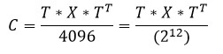
Where:
C - matrix of discrete cosine transform coefficients;
T is the transformation matrix;
X is a matrix of 8 by 8 brightness or monochromatic components (depending on which one, let's call it, the component plane Y, Cb or Cr is encoded).
For the reverse DCT, we obtain the following formula:
The coefficients of the matrix T in the eight-bit format are stored in the ROM located on the FPGA chip in the direct code, while the most significant bit contains the sign.
And so, at the first stage of the discrete cosine transform, from the SRAM memory to the operational block implementing the direct DCT, 64 bytes of one of the components are read (first the entire component plane Y is encoded, then Cb and Cr), forming part of the image, as was written earlier , 8 by 8 pixels in size (thus addresses for memory SRAM are generated in a special way):
Computation operations in this block are carried out with twenty one-digit data: 12 low-order digits — values that will be lost when divided by 4096 (2 ^ (12)), 8 digits — the significant part and high-order is the sign, total: 12 + 8 + 1 = 21:
Based on this, during loading, the eight-bit data in the operating unit is converted into twenty-one-bit words presented in the additional code by assigning the older thirteen bits filled with zero bits (the most significant bit is a sign), after which the resulting word is stored in the RAM buffer memory located Also, on the FPGA chip, into the address space from 00h to 3Fh (Quartus II did not allow creating RAM memory with the organization 128x21, so I had to use the memory with the organization 128x32).
At the second stage, after 64 twenty-one-bit words are written into the buffer RAM (block 8 by 8), the matrix multiplication process is started. , ROM , «» , () , ROM, () . , , , 7 – 19 :
, RAM , , , , . , :
, 8 . ( , ), , RAM, 40h 7Fh. , RAM, 40h – 7Fh, , , . ROM, , , , ( , , ). , , , , . , , .
. , , , ROM . :
Where:
R – , ;
i, j – , 0 7.
, Y, Cb, Cr , R = 2 ( , ).
, , :
Where:
a – , ;
b – , ;
c – .
, ROM -1 ( 1/b), , 8 , 0.
: , , , , 19 12 , 8 , , ( 11 0 , 4096).
, 0, 18 12 , 8 , , . 1616, ROM, , -1. , 8 , 8 – ROM.
, , 16 – , , 8 , , ( , – , ). , , 8, 7 , , , , :
, RAM 00h – 3Fh:
- ( - ) .
. : 6 – , 64, 8 – , 1 – . : 6+8+1 = 15:
, , , . , , , , 8 8 . , 7 7 , , , .
15- RAM 00h – 3Fh -. RAM 8 8, , . RAM, ( ) , ROM.
, ( , -1). , . 6 ( 64) , 0, 8 Y, Cb Cr ( , ). 1, 8 (.. 0, .. ).
RAM, , , 8 8. , SRAM , , , YCbCr.
, - , . – , :
, , , , , . .
, , , . 1, -1, , . 8 8, :
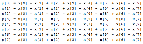
Where:
p[0..7] — ;
x[0..7] — , 8 8.
, , :
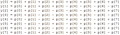
Where:
y[0..7] — ;
p[0..7] — .
, , , 0, 63 — , 0 ( ).
, , , , , , . , , 255, 64 6 .
, , 8 8 , .
, , , (6 — 64, 8 — , 1 — ) RAM. 8 8, , , , . RAM c 6415 ( 12821), Quartus II RAM 6416, ( 11 ).
, , , , , , RAM , -. , RAM -, , .
, , :
, , , , , RGB YCbCr, 8 8 . , . , , , , , , .
, -, , (RLE – Run Length Encoding). , ( ), , , .. < >< ()>. , ( ), , .
, , .pcx . RLE , -, , . , 0h . C0h, ( ), , , , , , 1h. , , , 63=3Fh, , , , 63, , , , FFh (C0h( -)+3Fh( ) = FFh), , .
, ( ) , RAM -: ECh, C2h, 03h, 0Ah, 0Ah, D1h, D1h, 01h, 01h, 01h, 00h, 00h, 00h, 00h, 00h, 02h, 00h, 00h, 00h, 00h, 00h, 00h, 00h, 00h, 00h, 00h, 00h, 00h, 00h, 00h, 00h, 00h, 00h, 00h, 00h, 00h, 00h, 00h, 00h, 00h, 00h, 00h, 00h, 00h, 00h, 00h, 00h, 00h, 00h, 00h, 00h, 00h, 00h, 00h, 00h, 00h, 00h, 00h, 00h, 00h, 00h, 00h, 00h, 00h. , , RLE, : C1h, ECh, C1h, C2h, 03h, C2h, 0Ah, C2h, D1h, C3h, 01h, C5h, 00h, 02h, F0h, 00h.
, , 64 , 16 , . , , , , , , , .
, - .
, , , , , , , , , , , , , .
, RLE , RLE, ( , ).
, , , , . , JPEG, , , , .
JPEG , JPEG , , , ROM , ROM, , . JPEG , , . ( ) , , .
: ROM, ( , RLE), , ROM, , , ROM. , .
, , . , , ROM, , 4 , – 11 , – 3, – 4. , 4+11+3+4 = 22, 22 8 2 6 , , , ( ) 3 , , .. .
, AHDL ( “TABLE”, , Verilog “case”, ), , .
: SRAM , , , ( ), , , .
, , , , , , , RLE. , , , ..
, , . , UART , 256 256 192 , () 8,1 .
, , . , () 43,8 .
, , . , UART , 256 256 192 , () 8,17 .
, , . , () 35,9 .
, , .
, , , – , , , – , , :

. , , , .
, . , — , – , , – :

, , , , 8 8, , , , – . , , .
, , , , , 256 256 .bmp (L.) 192 . : 256×256 = 65536 , (1 – , 1 – , 1 – ), 65536×3 = 196608 , 53 – , 196661 196661/1024 ≈ 192 «»:
, , , , , /. — . 1 — 0 .
, :
, , , . . : 2 — 0 .
, , , , .
, / , , , . ( , ) /. , , , (/) . , / — 24 , .
, . Thanks for attention!
First I want to thank the author of the articles "JPEG decoding for dummies" and "Inventing JPEG" , which greatly helped me in my work on writing this publication. When I took up the study of lossy image compression algorithms, then in part of the JPEG algorithm I was constantly tormented by the question: “Why is the role of the basic transformation in the JPEG algorithm specifically for the special case of the Fourier transform?”. Here the author gives an answer to this question, but I decided to approach it not from the point of view of a theory, mathematical models or software implementation, but from the point of view of circuit engineering.
The JPEG image compression algorithm is a digital signal processing algorithm, which, in hardware, is usually implemented either on digital signal processors or on programmable logic integrated circuits. In my case, the choice for the operation of a digital signal processor would mean coming to what I was trying to get away from - to a software implementation, so it was decided to stop at a programmable logic.
In one of the online stores, I purchased a fairly simple debug board , which contains Altera FPGA Cyclone 4 -EP4CE6E22 FPGA and SRAM 512Kx8 memory. Since the FPGA was from Altera, it was decided to use the Quartus II Web Edition environment for development. Development of individual functional blocks of the hardware codec was carried out in the Verilog language , and assembly into a single scheme was carried out in the graphical editor of the Quartus II Web Edition environment.
')
To communicate with a personal computer (receiving commands, receiving / transmitting the processed data), in Verilog I wrote a simple asynchronous UART transceiver. To connect to the COM-port ( RS-232 ) of the computer, based on the MAX3232WE chip and from what was at hand, hastily, the level converter was soldered. In the end, here's what happened:
For sending commands from a personal computer, as well as receiving and transmitting data, a trial version of the ADVANCED SERIAL PORT MONITOR program was used, which allows you to create not only individual parcels of data bytes, but also generate data streams from the file contents, and also record received data streams to a file, which allowed to send and receive files. I do not use and control any protocols and checksums for receiving / transmitting data via UART (I was simply too lazy to envisage and implement all this); during the communication for receiving / transmitting, I used what is called “raw data”.
All arithmetic operations associated with fractional numbers in the codec are carried out in a fixed-point format, addition and subtraction operations are carried out in an additional code , in principle this is understandable. How the bit depth of the processed data was determined will be described below.
The compression operation is performed on the source images presented in the .bmp format with a color depth of 24 bits per pixel (8 bits for each of the color components).
The memory available on the debug board was organized as follows: addresses from 00000h to 3FFFFh (in hexadecimal numbering system ) were allocated for storing source data (picture in .bmp format for compression, or coded data for unpacking), totaling 256 KB, the remaining 256 KB space for recording received, as a result of data compression or decompression, these are addresses from 40000h to 7FFFFh. I think it is obvious that the maximum size of compressible images is limited by the amount allocated for data storage, memory.
The algorithm of the device operation is as follows: immediately after the power supply, the codec waits for a data stream via the UART, any data received, while the data is interpreted as an initial file for processing, if the pause between bytes is 10 ms, then this is interpreted as the end of the file and following the pause Bytes received by the UART are perceived by the device as a command. Commands are specific byte values. For example, after receiving a file after 10 ms, received by the UART codec, the value of byte AAh is interpreted by the device as a command that sends data from the memory chip to the computer via the UART, starting at address 40000h and ending with the value of the address at which the processed data was written i.e. The results of compression / decompression are transmitted to the computer. The value of EEh is interpreted as a command for compressing / decompressing an image, and also for debugging I provided a number of other commands.
As for the structure of the file with the compressed image, then I decided not to bother, and, in contrast to the JPEG algorithm, the algorithm I implement is rather narrowly targeted and not designed for all occasions, therefore, the resulting data as a result of compression the stream is written to the allocated memory area. The only thing that needs to be noted here is that in order not to implement the header generator for the .bmp file (it was also lazy), during compression, it is simply completely rewritten to the initial (from the address 40000h) memory area reserved for the final data, and then, starting with the offset from which pixel data is stored in the source .bmp file, compressed data is written. This offset is stored in the header of the .bmp file at 0Ah relative to its beginning, and is typically 36h. When unpacking, the same operation is performed accordingly.
So, image compression of JPEG-like algorithms is performed in the following sequence:
- color space conversion from RGB to YCbCr or YUV ;
- color downsampling ;
- base transform;
- quantization of coefficients obtained after the base transformation;
- zigzag scanning;
- run length coding ;
- Huffman compression.
Unpacking is in reverse order.
Of all the steps listed above, in the codec, I did not implement sub-sampling, as I considered it superfluous (maybe I’m wrong).
Based on the above sequence of actions, I developed the following functional codec scheme:
The codec operation process is controlled by a control device, which is a finite state machine, here the coding / decoding of run lengths is performed, as well as the generation of final data from Huffman codes during compression and the formation of the Huffman codes themselves from data received from the SRAM memory during unpacking. The control unit also generates control signals for other operating units.
Under the main circuit, there are diagrams of operating units, changing them in the main circuit, I changed the modes of operation of the device. There was an attempt to collect everything into a single device and set the modes of operation of the codec, as well as methods of basic transformation using the commands on the UART, but the logical capacity of the FPGA was not enough. Therefore, the operation modes of the device are changed by changing the corresponding operational blocks and the task of certain parameters in the control device (including the size of the compressible / unpacked image), after which the modified project is compiled and stitched into the FPGA.
Color Space Conversion
On the Internet you can find a lot of different information on the transformation of color spaces, so I will immediately begin with a description of the hardware implementation.
The color space conversion block is a combinational logic, due to which the color components are transformed in one generator cycle. The conversion of the RGB color space to YCbCr is performed by the following formulas:
The calculation begins with the control device setting the starting address of the SRAM memory chip to the starting address from which the pixel data is stored in the .bmp file, as mentioned above, the starting address is 36h. The .bmp files at this address store the value of the blue color component of the lowest right pixel of the image. At address 37h, the value of the green color component, then red, then the blue component of the next pixel in the bottom line of the image again, etc. As you can see from the functional diagram, there is a register for each color component in the scheme. After loading from memory all three color components into their registers, from the next clock of the generator recording of the results of calculations is carried out in memory. So, the monochromatic red component “Cr” is recorded at the address of the blue component “B”, the monochromatic blue component “Cb” is recorded at the address of the green component “G”, and the component “Y” is recorded at the address “R”. As a result of this step, the same image in YCbCr format will appear in place of the original image in the SRAM memory in RGB format.
For the hardware implementation of calculations of the brightness and monochromatic components, all fractional coefficients from the formulas were presented in the form of sixteen-bit words in a fixed-point format, where the upper eight bits contain an integer part, respectively, the lower eight bits have a fractional part. For example, the coefficient 0.257 in binary representation with a fixed point looks like this: 0000000001000001 or in hexadecimal form 0041h. The limited number of digits reduces the accuracy, so if the fractional binary number 0000000001000001 is converted to decimal form, we get: 2 ^ (- 2) + 2 ^ (- 8) = 0.25 + 0.00390625 = 0.25390625. As you can see, the result differs from the value of 0.257 and in order to improve the accuracy of the presentation, the number of digits allocated for the fractional part should be increased. But I decided to limit, as mentioned above, to eight digits.
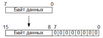
So, in the first stage of the conversion, the eight-bit values of the RGB color components are converted to sixteen-bit in a fixed-point format by adding eight low-order bits filled with zero bits:
At the second stage, multiplication, addition and / or subtraction operations are carried out. As a result, thirty-two-bit data is obtained, where the sixteen senior digits contain an integral part, and the sixteen low-order ones contain fractional part.
In the third stage, eight-bit data is formed from the thirty-two-digit words obtained by selecting eight bits immediately before the comma (if the lowest-order bit is 0 and the oldest is 31, then these are bits 23 to 16):
At the fourth stage, to the obtained eight-bit words, in accordance with the above-presented formulas, offsets are added (for component Y - 16, for components Cb, Cr - 128).
Conversion from YCbCr to RGB is carried out according to the following formulas:
Here there is such a feature that the results of calculations, in some cases, can acquire values greater than 255, which goes beyond one byte, or negative values, respectively, such situations need to be monitored.
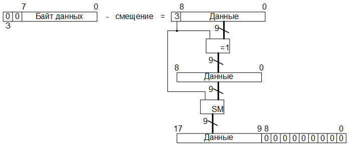
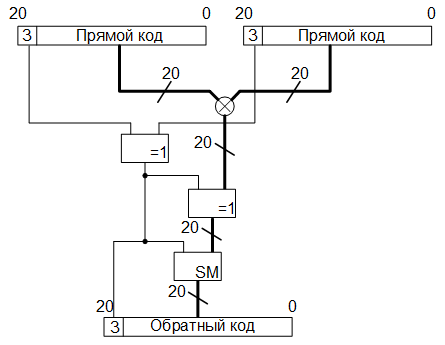
So, if an overflow occurs, the value of the resulting color component should be equal to 255; for this, we simply perform a bitwise logical OR operation of the result with an overflow bit. And if the sign digit of the result is equal to one (i.e., the value is less than zero), then the value of the final color component should be 0, for this, we perform a bitwise logical operation “AND” of the result with the inverted value of the sign bit.
So, at the first stage of converting the YCbCr color space into RGB, read from the SRAM memory chip, we translate the eight-bit values of the luminance and monochromatic components into an additional ten-bit code, by adding two high-order zero bits (the sign bit and the overflow flag). As a result, we get ten-bit words. Further, in accordance with the formulas, we subtract from these values of the offset (or add the negative values of the offsets presented in the ten-bit additional code). Then, we translate the result obtained from the additional code into the straight line, preserving the values of the highest (sign) bit. The remaining nine-bit words will be converted to eighteen-bit with a fixed point path, attributing the lower nine bits with zero bits:
Fractional coefficients appearing in the formulas are also represented in the form of an eighteen-bit code with a fixed point, where 9 bits are allocated for the integral and fractional parts. As a result of multiplication operations, we get thirty-six-bit values of products, in which 18 high-order bits - the whole part, 18 low-order bits - fractional. Then we calculate the sign of the product by performing a logical operation “addition modulo 2”, a previously stored sign bit with a sign before the coefficient in the formula (if “-”, then “1”, if “+”, then “0”).
It is also necessary to determine whether the result of the product is zero, if the result of multiplication is zero, then 0 must be written in the sign bit, regardless of the signs before the coefficients and the signs of the results obtained as a result of the offset of the components read from the memory. To do this, apply the reduction operator (| product [35: 0]) to the product, which determines whether all the bits are equal to zero as a result of multiplication (if so, the result of the operation of this operator will be zero), and then perform a logical AND operation the result obtained with the result of the operation "addition modulo 2" sign digits.
After all this, we translate the results of the multiplication into an additional thirty-seven-digit code, where the sign is stored in the most significant digit, and perform addition operations. After the addition operations, obtained in the additional code, we translate the results into a direct code, and select eight bits immediately before the comma (if the number of the least significant bit 0 and the most significant one is 36, then these are bits 25 to 18). Next, we check if there was an overflow; for this, as mentioned above, we perform a bitwise logical “OR” operation of eight bits allocated with an overflow sign, which is stored in the 26th digit. And yet, we check whether a negative result is obtained, for which we perform a bitwise logical operation of the “And” of an inverted sign bit with the same eight bits:
The resulting, calculated by three formulas, and the converted eight-bit values are the values of the RGB color components.
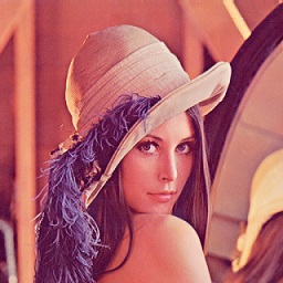
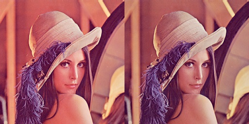
I decided to test the device using a 256 by 256 pixel photo of Lena Soderberg:
Everyone working in image processing works with this photo, and I decided not to be an exception.
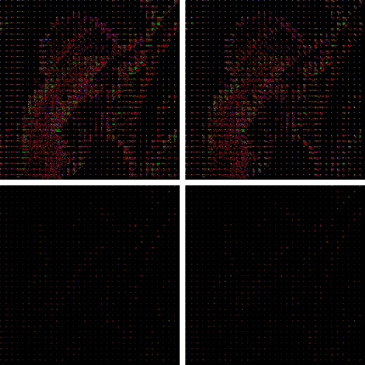
So, as a result of the conversion of the original photo loaded on the UART to the SRAM memory of the debug board, from the RGB color space to the YCbCr space, the following image was obtained:
The picture below shows the original photo on the right, the photo on the left is the result of the inverse transformation from the YCbCr space into the RGB color space as described above:
When comparing the original and transformed photographs, you can see that the original photograph is brighter than the processed one, this is due to the loss of data that occurred during rounding (“garbage” of the fractional part), as well as loss of accuracy, when representing fractional coefficients in binary form.
Basic transforms and quantization coefficients
Discrete cosine transform
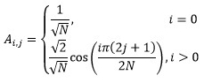
Information about what a discrete cosine transform (hereinafter referred to as DCT), on the Internet is present in sufficient quantity, so I’ll dwell briefly on the theory.
As mentioned in this publication, the essence of any basic transformation is reduced to multiplying the transformation matrix by the input data matrix, after which the result is again multiplied by the transposed matrix of the same transformation. In the case of a discrete cosine transform, the coefficients of the transform matrix are calculated according to the following rule:
Where:
N is the dimension of the matrix;
i, j - indices of matrix elements.
In our case, N = 8, i.e. the original image is divided into blocks of 8 by 8 pixels, while the values of the indices i and j vary in the range from 0 to 7.
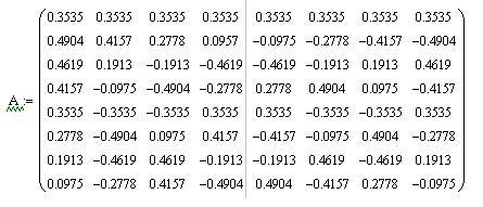
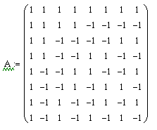
As a result of applying this rule for N = 8, we obtain the following transformation matrix:
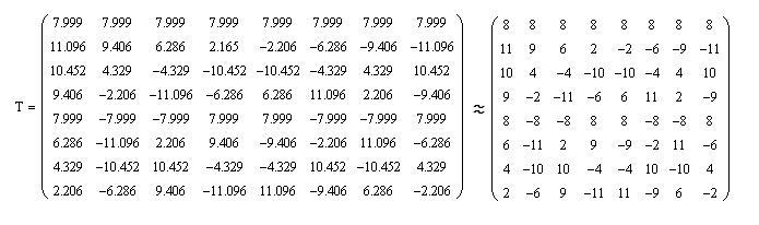
In order not to carry out calculations with fractional numbers, we multiply each element of the matrix by 8√8, and round the obtained values of the elements of the matrix to integers, with the result that we get the matrix T:
In this case, it will be necessary to divide the result of matrix multiplication, as in the case of direct discrete cosine transform when encoding, and in the case of the opposite when decoding, divided by 512. Given that 512 = 2 ^ (9), then division is done by shifting the dividend to the right by 9 positions.
As a result of the direct discrete cosine transform, a matrix is obtained of the so-called DCT coefficients, in which the element located in the zero row and the zero column is called the low-frequency coefficient and its value is always positive. The remaining elements of the DCT matrix are high-frequency coefficients, the values of which can be either positive or negative. Considering this, and the fact that the elements of the resulting matrix must be eight-bit, for the low-frequency coefficient the range of values will be [0..255], and for high-frequency - [-127..127]. In order to meet these ranges, it is necessary to divide the results of the direct discrete cosine transform by 8, respectively, the results of the reverse are multiplied by 8. As a result, for the direct DCT we get the following formula:
Where:
C - matrix of discrete cosine transform coefficients;
T is the transformation matrix;
X is a matrix of 8 by 8 brightness or monochromatic components (depending on which one, let's call it, the component plane Y, Cb or Cr is encoded).
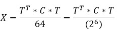
For the reverse DCT, we obtain the following formula:
The coefficients of the matrix T in the eight-bit format are stored in the ROM located on the FPGA chip in the direct code, while the most significant bit contains the sign.
And so, at the first stage of the discrete cosine transform, from the SRAM memory to the operational block implementing the direct DCT, 64 bytes of one of the components are read (first the entire component plane Y is encoded, then Cb and Cr), forming part of the image, as was written earlier , 8 by 8 pixels in size (thus addresses for memory SRAM are generated in a special way):
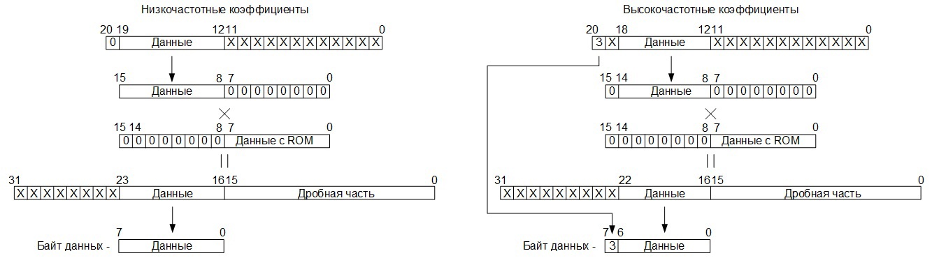
Computation operations in this block are carried out with twenty one-digit data: 12 low-order digits — values that will be lost when divided by 4096 (2 ^ (12)), 8 digits — the significant part and high-order is the sign, total: 12 + 8 + 1 = 21:
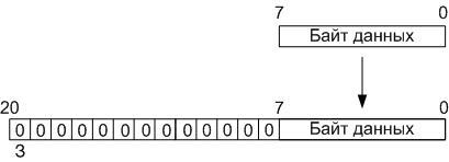
Based on this, during loading, the eight-bit data in the operating unit is converted into twenty-one-bit words presented in the additional code by assigning the older thirteen bits filled with zero bits (the most significant bit is a sign), after which the resulting word is stored in the RAM buffer memory located Also, on the FPGA chip, into the address space from 00h to 3Fh (Quartus II did not allow creating RAM memory with the organization 128x21, so I had to use the memory with the organization 128x32).
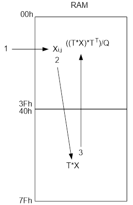
At the second stage, after 64 twenty-one-bit words are written into the buffer RAM (block 8 by 8), the matrix multiplication process is started. , ROM , «» , () , ROM, () . , , , 7 – 19 :
, RAM , , , , . , :
, 8 . ( , ), , RAM, 40h 7Fh. , RAM, 40h – 7Fh, , , . ROM, , , , ( , , ). , , , , . , , .
. , , , ROM . :
Where:
R – , ;
i, j – , 0 7.
, Y, Cb, Cr , R = 2 ( , ).
, , :
Where:
a – , ;
b – , ;
c – .
, ROM -1 ( 1/b), , 8 , 0.
: , , , , 19 12 , 8 , , ( 11 0 , 4096).
, 0, 18 12 , 8 , , . 1616, ROM, , -1. , 8 , 8 – ROM.
, , 16 – , , 8 , , ( , – , ). , , 8, 7 , , , , :
, RAM 00h – 3Fh:
- ( - ) .
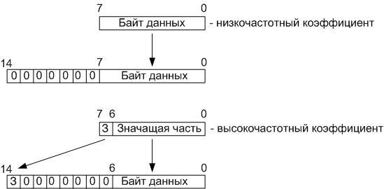
. : 6 – , 64, 8 – , 1 – . : 6+8+1 = 15:
, , , . , , , , 8 8 . , 7 7 , , , .
15- RAM 00h – 3Fh -. RAM 8 8, , . RAM, ( ) , ROM.
, ( , -1). , . 6 ( 64) , 0, 8 Y, Cb Cr ( , ). 1, 8 (.. 0, .. ).
RAM, , , 8 8. , SRAM , , , YCbCr.
, - , . – , :
, , , , , . .
, , , . 1, -1, , . 8 8, :
Where:
p[0..7] — ;
x[0..7] — , 8 8.
, , :
Where:
y[0..7] — ;
p[0..7] — .
, , , 0, 63 — , 0 ( ).
, , , , , , . , , 255, 64 6 .
, , 8 8 , .
, , , (6 — 64, 8 — , 1 — ) RAM. 8 8, , , , . RAM c 6415 ( 12821), Quartus II RAM 6416, ( 11 ).
, , , , , , RAM , -. , RAM -, , .
, , :
, , , , , RGB YCbCr, 8 8 . , . , , , , , , .
Series Length Coding
, -, , (RLE – Run Length Encoding). , ( ), , , .. < >< ()>. , ( ), , .
, , .pcx . RLE , -, , . , 0h . C0h, ( ), , , , , , 1h. , , , 63=3Fh, , , , 63, , , , FFh (C0h( -)+3Fh( ) = FFh), , .
, ( ) , RAM -: ECh, C2h, 03h, 0Ah, 0Ah, D1h, D1h, 01h, 01h, 01h, 00h, 00h, 00h, 00h, 00h, 02h, 00h, 00h, 00h, 00h, 00h, 00h, 00h, 00h, 00h, 00h, 00h, 00h, 00h, 00h, 00h, 00h, 00h, 00h, 00h, 00h, 00h, 00h, 00h, 00h, 00h, 00h, 00h, 00h, 00h, 00h, 00h, 00h, 00h, 00h, 00h, 00h, 00h, 00h, 00h, 00h, 00h, 00h, 00h, 00h, 00h, 00h, 00h, 00h. , , RLE, : C1h, ECh, C1h, C2h, 03h, C2h, 0Ah, C2h, D1h, C3h, 01h, C5h, 00h, 02h, F0h, 00h.
, , 64 , 16 , . , , , , , , , .
, - .
, , , , , , , , , , , , , .
, RLE , RLE, ( , ).
, , , , . , JPEG, , , , .
JPEG , JPEG , , , ROM , ROM, , . JPEG , , . ( ) , , .
: ROM, ( , RLE), , ROM, , , ROM. , .
, , . , , ROM, , 4 , – 11 , – 3, – 4. , 4+11+3+4 = 22, 22 8 2 6 , , , ( ) 3 , , .. .
, AHDL ( “TABLE”, , Verilog “case”, ), , .
: SRAM , , , ( ), , , .
, , , , , , , RLE. , , , ..
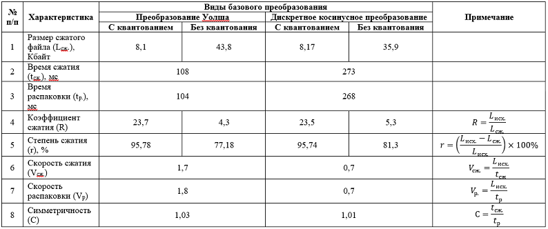
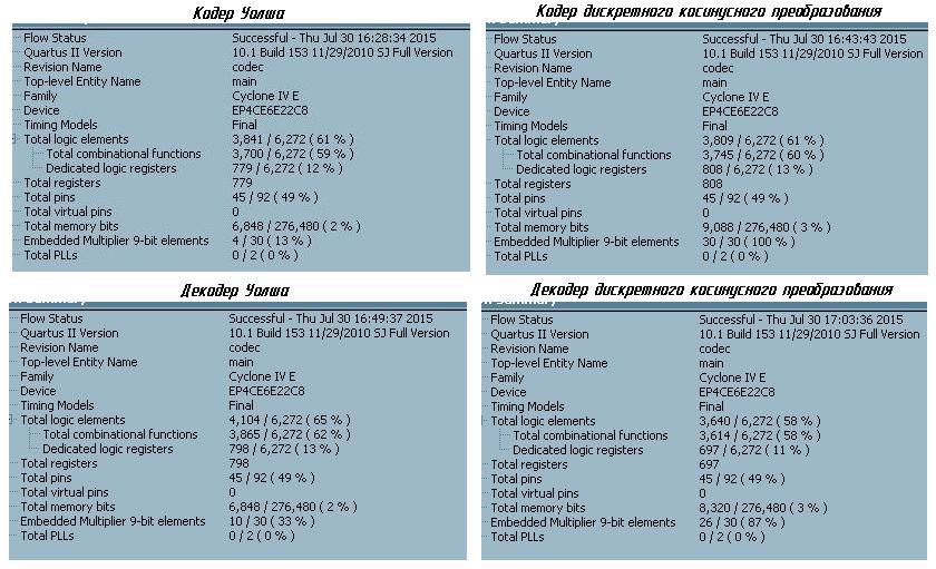
, , . , UART , 256 256 192 , () 8,1 .
, , . , () 43,8 .
, , . , UART , 256 256 192 , () 8,17 .
, , . , () 35,9 .
, , .
, , , – , , , – , , :
. , , , .
, . , — , – , , – :
, , , , 8 8, , , , – . , , .
Summarizing
, , , , , 256 256 .bmp (L.) 192 . : 256×256 = 65536 , (1 – , 1 – , 1 – ), 65536×3 = 196608 , 53 – , 196661 196661/1024 ≈ 192 «»:
, , , , , /. — . 1 — 0 .
, :
, , , . . : 2 — 0 .
, , , , .
, / , , , . ( , ) /. , , , (/) . , / — 24 , .
, . Thanks for attention!
Source: https://habr.com/ru/post/264739/
All Articles