SoC: we write framebuffer implementation for controller in FPGA
Greetings
Last time, we stopped by raising DMA to FPGA.
Today we are implementing a primitive LCD controller in the FPGA and write a framebuffer driver for working with this controller.
')
You will once again make sure that developing for FPGA and writing drivers for Linux is very simple, but interesting.
Also at the end there is a small survey - I want to know the opinion of the community. If not difficult, please vote.
It so happened that in HPS on Cyclone V there is no integrated graphics controller. And we can’t live without a display - where to take the measurement results .
Of course, you can do without the software implementation of the framebuffer (with the addition of all sorts of usefulness in the form of deferred_io and double buffering). But it, all the same, will not be very bright and definitely will not be as interesting as what we choose.
And we choose the implementation of a very simple, but fully working LCD controller in the FPGA, which will remove the unnecessary load from the CPU in the form of writing data to the display.
We will use LCD based on the ILI9341 chip.
So, plan for today:
- Thinking about architecture
- We study our LCD
- Writing Linux Driver
- Developing a module in FPGA
- Configuring something in the U-boot
- Debugging
Architecture
What is a framebuffer in Linux?
In a nutshell - this is just a memory area, writing to which results in the display of what is written on the display.
From userspace, access is performed through the device file / dev / fb [N] .
Standard system calls are usually implemented - open (), close (), read (), write (), lseek () and mmap ().
In the driver, most of the functions perform one task - to update a frame that is stored in memory.
Sometimes there are also functions that copy data from the memory to the LCD, if this is not implemented in hardware.
All structures and functions are well described in detail in these articles - a link once and a link two .
There is no sense to duplicate information, so we will analyze only what affects our architecture.
So, we have several functions that are designed to update data in memory. They have a slightly different signature. Using these functions, you can redraw both the entire frame or just a few pixels.
After updating the frame, you need to make it hit the LCD. Naturally, copying only the modified part of the frame requires a smaller amount of data to be transferred. And if we copied the data using the CPU, then we would definitely be worth considering.
But we will copy the DMA controller in the FPGA, so we will not worry about it and will redraw the entire frame.
The next question is when to redraw the frame. One simple solution is to perform drawing synchronously, that is, at the end of each function that updates the data in memory. This works well in all cases except using mmap ().
After the mapping is complete, it is not so easy to determine when the userspace process has changed the contents of the memory. This task can be solved with the help of deferred_io (and at the same time you can identify specific pages of memory that have been updated and need to be redrawn). But we want our implementation to be as simple and clear as possible, so we will do it differently.
Our controller in the FPGA will render the entire frame at a frequency of n FPS. And it will do it asynchronously with respect to updating memory driver functions. Thus, all that needs to be done in the driver is the initialization of the LCD and FPGA controller. And even we will not need to implement the data recording in the memory of the framebuffer, for this we already have standard functions.
The controller in the FPGA will also be fairly simple. His tasks:
- Read data from the specified area on the interface fpga2sdram or fpga2hps
- Transfer read data to LCD, forming the necessary transactions
- Enable the CPU to directly access the interface to the LCD
- Issue the specified FPS
Description of our LCD
All we need to know about the LCD is how to initialize it and what the write transaction looks like.
Initialization will be considered when we get to the driver, and now we will study the transaction.
We will have to implement them both in FPGA (for data transfer) and in the driver (for adjusting the display).
ILI9341 supports multiple interfaces. I use a parallel 16-bit interface called 8080 by the name of the Intel processor in which it first appeared. Here are the signals that are there (the more common name is first indicated, and the name from the datasheet on ILI9341 is shown in brackets):
- CS (CSX) - chip-select, active level 0. The chip select signal, I have got to the ground.
- RST (RESX) - reset, active level 0. Reset signal, I have got a GPIO HPS.
- RS (D / CX) - register select. If the signal is 0, then a command is issued on the DATA bus, otherwise, the data.
- WR (WRX) - write strobe. Strobe entry.
- RD (RDX) - read strobe. Strobe reading.
- DATA (D) - data or command, depending on the RS.
The write transaction is extremely simple:
Write transaction

The read transaction is not more difficult, but we will not need it, so we will not consider it.
Linux driver
What do we have in the driver?
First, the functions for reading / writing FPGA registers. You can read more about what status control registers are and how to use them, see my ishevchuk colleague’s article .
CSR read / write functions
static void fpga_write_reg(int reg, u16 val) { iowrite16(val, fpga_regs + 2*reg); } static u16 fpga_read_reg(int reg) { u16 tmp; tmp = ioread16(fpga_regs + 2*reg); return tmp; } static void fpga_set_bit(int reg, int bit) { unsigned long tmp = fpga_read_reg(reg); set_bit(bit, &tmp); fpga_write_reg(reg, tmp); } static void fpga_clear_bit(int reg, int bit) { unsigned long tmp = fpga_read_reg(reg); clear_bit(bit, &tmp); fpga_write_reg(reg, tmp); } Secondly, the functions for direct recording in the LCD commands and data. They will be used to initialize the display.
The functions are absolutely “clumsy” - we simply make the transaction as it is shown in the datasheet (and later in this article).
LCD data / command write functions
static void lcd_write_command(u16 val) { /* Write command code */ fpga_write_reg(LCD_DATA_CR, val); /* WR and RS low, RD high */ fpga_write_reg(LCD_CTRL_CR, LCD_CTRL_CR_RD); ndelay(1); /* RS low, WR and RD high */ fpga_write_reg(LCD_CTRL_CR, LCD_CTRL_CR_RD | LCD_CTRL_CR_WR); ndelay(1); /* All control signals high */ fpga_write_reg(LCD_CTRL_CR, LCD_CTRL_CR_RD | LCD_CTRL_CR_WR | LCD_CTRL_CR_RS); } static void lcd_write_data(u16 data) { /* Write data */ fpga_write_reg(LCD_DATA_CR, data); /* WR low, RD and RS high */ fpga_write_reg(LCD_CTRL_CR, LCD_CTRL_CR_RD | LCD_CTRL_CR_RS); ndelay(1); /* All control signals high */ fpga_write_reg(LCD_CTRL_CR, LCD_CTRL_CR_RD | LCD_CTRL_CR_RS | LCD_CTRL_CR_WR); } Well and, actually, our simple initialization LCD.
LCD initialization function
static void lcd_init(struct fb_info *info) { // Clear data fpga_write_reg(LCD_DATA_CR, 0); // All control signals high fpga_write_reg(LCD_CTRL_CR, LCD_CTRL_CR_RD | LCD_CTRL_CR_RS | LCD_CTRL_CR_WR); mdelay(100); lcd_write_command(ILI9341_DISPLAY_ON); lcd_write_command(ILI9341_SLEEP_OUT); lcd_write_command(ILI9341_INVERTION_OFF); lcd_write_command(ILI9341_MEM_ACCESS_CTRL); lcd_write_data(MY | MX | MV | BGR); lcd_write_command(ILI9341_PIXEL_FORMAT); lcd_write_data(0x0055); lcd_write_command(ILI9341_COLUMN_ADDR); lcd_write_data(0x0000); lcd_write_data(0x0000); lcd_write_data((DISPLAY_WIDTH-1) >> 8); lcd_write_data((DISPLAY_WIDTH-1) & 0xFF); lcd_write_command(ILI9341_PAGE_ADDR); lcd_write_data(0x0000); lcd_write_data(0x0000); lcd_write_data((DISPLAY_HEIGHT-1) >> 8); lcd_write_data((DISPLAY_HEIGHT-1) & 0xFF); lcd_write_command(ILI9341_MEM_WRITE); } Briefly about the commands used.
ILI9341_DISPLAY_ON (0x29) and ILI9341_SLEEP_OUT (0x11), although unexpected, turn on the display and take it out of sleep mode.
ILI9341_MEM_ACCESS_CTRL (0x36) is the setting for the direction of memory scanning.
ILI9341_PIXEL_FORMAT (0x3a) is an image format, we have 16 bits per pixel.
ILI9341_COLUMN_ADDR (0x2a) and ILI9341_PAGE_ADDR (0x2b) define the working area of our display.
ILI9341_MEM_WRITE (0x2c) - this command says that data transactions will follow. In this case, the current position is set to the initial column and row, which were set, respectively, using ILI9341_COLUMN_ADDR and ILI9341_PAGE_ADDR. After each transaction, the column will automatically increment by 1. When the column becomes equal to the final one, a transition to the next row will occur. When both the column and the row become equal to the end position, the position returns to the initial one.
Thus, after the ILI9341_MEM_WRITE command, the controller in the FPGA can simply “in a circle” send data from the memory to the LCD without worrying about anything else.
The last thing that interests us in the driver is the probe function.
Driver probe function
struct fb_info *info; int ret; u32 vmem_size; unsigned char *vmem; dma_addr_t dma_addr; pdev->dev.dma_mask = &platform_dma_mask; pdev->dev.coherent_dma_mask = DMA_BIT_MASK(32); vmem_size = (etn_fb_var.width * etn_fb_var.height * etn_fb_var.bits_per_pixel) / 8; vmem = dmam_alloc_coherent(&pdev->dev, vmem_size, &dma_addr, GFP_KERNEL); if (!vmem) { dev_err(&pdev->dev, "FB: dma_alloc_coherent error\n"); return -ENOMEM; } memset(vmem, 0, vmem_size); info = framebuffer_alloc(0, &pdev->dev); if (!info) return -ENOMEM; info->screen_base = vmem; info->fbops = &etn_fb_ops; info->fix = etn_fb_fix; info->fix.smem_start = dma_addr; info->fix.smem_len = vmem_size; info->var = etn_fb_var; info->flags = FBINFO_DEFAULT; info->pseudo_palette = &etn_fb_pseudo_palette; /* Get FPGA registers address */ fpga_regs = devm_ioremap(&pdev->dev, FPGA_REGS_BASE, REGSIZE); /* Disable refreshing */ fpga_write_reg(LCD_DMA_CR, 0); lcd_init(info); set_dma_addr(dma_addr); set_fps(fps); /* Enable refreshing */ fpga_set_bit(LCD_DMA_CR, LCD_DMA_CR_REDRAW_EN); ret = register_framebuffer(info); if (ret < 0) { framebuffer_release(info); return ret; } platform_set_drvdata(pdev, info); return 0; What is happening in it?
First, we allocate memory in a DMA-compatible zone using the dmam_alloc_coherent () function. In this case, we get two addresses that "point" to the selected area. One will be used in the driver, and the second we will write a FPGA so that the DMA controller can read data from this area.
A few words about DMA mappings. They are of two types:
- Streaming
- Matched (Coherent or Consistent)
Consistent mappings are available simultaneously to the processor and device. Upon access, each party is guaranteed to receive “fresh” data. Most often used when a buffer exists throughout the life of the driver. An example of use is our framebuffer memory.
When using stream mappings, access is possible strictly in turn. Most often created at the time of a single operation.
Theoretically, it can be more productive. An example is receiving / sending network packets.
Let's go back to the probe function. Next we fill in fb_info .
Then we map the FPGA address space in order to be able to read and write to the control status registers.
After that we write the required FPS value and our DMA-address in the FPGA (remembering to translate it into the word number, if necessary).
Then we turn on the drawing in FPGA and register our framebuffer. All is ready!
FPGA module
We got to the module in the FPGA. Here, too, everything is simple.
Let me remind you that we need to implement:
- Direct CPU access to the LCD
- Reading framebuffer memory
- Forming transaction records in the direction of the LCD
- Getting the right FPS
To ensure direct access of the CPU to the LCD, we naturally will use control registers.
And the usual multiplexer - when control comes from the CPU, signals from the registers are switched to the LCD interface, otherwise signals from the module to the FPGA. The selection occurs depending on the state of the finite state machine, which is described below.
Primitive code:
LCD bus MUX
always_ff @( posedge clk_i ) if( state == IDLE_S ) begin lcd_bus_if.data <= lcd_ctrl_if.data; lcd_bus_if.rd <= lcd_ctrl_if.rd; lcd_bus_if.wr <= lcd_ctrl_if.wr; lcd_bus_if.rs <= lcd_ctrl_if.rs; end else // Send data transactions from FPGA. begin lcd_bus_if.data <= lcd_data_from_fpga; lcd_bus_if.rd <= 1'b1; lcd_bus_if.wr <= lcd_wr_from_fpga; lcd_bus_if.rs <= 1'b1; end The next task is to read the data from the memory and write it to the LCD. Here you need to think a little.
We cannot continuously read data, since the reading interface's bandwidth is much greater than the speed at which we will write data to the LCD (remember that we need to comply with the timeframes specified in the documentation).
That is, we need to artificially limit the speed of reading. There are the following options for this:
- Read and write to the LCD in sequence - read, write, read, write, etc.
- Calculate the speed with which we need to read data, and maintain it
- Use FIFO
The first option will lead to the fact that the data on the LCD will come with large (by the FPGA standards) pauses.
Considering the applied task (we hardly need to get an FPS greater than 50), it is quite possible that this is enough for us.
But it is too clumsy and ugly. Therefore, this option is dismissed.
The second option is to calculate the speed at which data should be read from memory, so that we can get a continuous stream to the LCD. It is also quite a working option, especially considering that we have no strict requirements for the constancy of the output flow rate. But, in general, due to the variable latency in read transactions, we would still have to use a buffer for rate matching.
The third option is very simple and fairly reliable. Its essence is that we use a FIFO - a buffer in which we write read data from memory at high speed. When in the buffer the place comes to an end we suspend reading. At the same time, we can continuously read data from the buffer and form transactions on the LCD at a constant speed. As soon as a place appears in the FIFO, we again resume reading from the memory.
We choose the third option. First we need a FIFO:
FIFO instance
buf_fifo #( .AWIDTH ( FIFO_AWIDTH ), .DWIDTH ( AMM_DATA_W ) ) buf_fifo ( .clock ( clk_i ), .aclr ( ), .wrreq ( fifo_wr_req ), .data ( fifo_wr_data ), .rdreq ( fifo_rd_req ), .q ( fifo_rd_data ), .almost_full ( ), .full ( ), .empty ( fifo_empty ), .usedw ( fifo_usedw ) ); To determine the moment of suspension of reading it is not enough to know how the FIFO is already filled. After all, we also have read transactions that are now “in progress.” That is, the data, the reading of which we have already requested, but which have not yet been delivered to us.
We need to know the number of such transactions at the moment. To do this, each time a read request is executed, we will increase the corresponding counter, and when we receive confirmation of the read data, decrease it.
Pending transactions calculation
// Count of read transactions in progress logic [FIFO_AWIDTH-1:0] pending_read_cnt; always_ff @( posedge clk_i ) case( { read_req_w, amm_if.read_data_val } ) 2'b01: pending_read_cnt <= pending_read_cnt - 1'd1; 2'b10: pending_read_cnt <= pending_read_cnt + 1'd1; endcase As a result, we will stop reading when the amount of words and transactions “in process” recorded in the FIFO is almost equal to the depth of our queue. As “almost” we will choose 50 free words:
Stop reading
logic stop_reading; assign stop_reading = ( pending_read_cnt + fifo_usedw ) > ( 2**FIFO_AWIDTH - 'd50 ); Forming read transactions themselves on Avalon MM is primitive. The main thing is to increment the address correctly depending on the type of interface: fpga2sdram or fpga2hps (for a more detailed description of the interfaces and differences, see here ):
Read transactions
// fpga2sdram used word address, so we must added 1 every time, // fpga2hps used byte address, so we must added 8 (for 64-bit iface). logic [31:0] addr_incr; assign addr_incr = ( USE_WORD_ADDRESS == 1 ) ? 1 : ( AMM_DATA_W >> 3 ); always_ff @( posedge clk_i ) if( state == IDLE_S ) amm_if.address <= lcd_ctrl_if.dma_addr; else if( read_req_w ) amm_if.address <= amm_if.address + addr_incr; // Always read all bytes in word assign amm_if.byte_enable = '1; // We don't use burst now assign amm_if.burst_count = 1; assign amm_if.read = ( state == READ_S ); // Remove Quartus warnings assign amm_if.write_data = '0; assign amm_if.write = 0; We learned to read the data, now we need to learn how to write them in LCD. To do this, we will make a simple finite state machine for two states: if there is data in the FIFO, the automaton changes to the sending transaction state. And after the end of the recording, it returns to IDLE:
FSM for writing to LCD
enum int unsigned { LCD_IDLE_S, LCD_WRITE_S } lcd_state, lcd_next_state; always_ff @( posedge clk_i ) lcd_state <= lcd_next_state; always_comb begin lcd_next_state = lcd_state; case( lcd_state ) LCD_IDLE_S: begin if( !fifo_empty ) lcd_next_state = LCD_WRITE_S; end LCD_WRITE_S: begin if( lcd_word_cnt == 5'd31 ) lcd_next_state = LCD_IDLE_S; end endcase end assign fifo_rd_req = ( lcd_state == LCD_IDLE_S ) && ( lcd_next_state == LCD_WRITE_S ); It must be remembered that one transaction before the LCD is the transmission of 16 bits of data, and each word in the FIFO has a size of 64 bits (depending on the interface settings of fpga2sdram / fpga2hps). Therefore, for each word read, we will form 4 transactions.
It is simple to form them - for this we only need to make one counter and use the necessary digits in it:
Read transactions
// ILI9341 Data transaction from FPGA: // __ __ __ __ __ __ __ __ __ // clk/4 | __| |__| |__| |__| |__| |__| |__| |__| |__| | // // data | ///< split[0] | split[1] | split[2] | split[3] >//// // // _______________________________________________ // rd | xxxx xxxx // // _____ _____ _____ _____ // wr | xxxx_____| |_____| |_____| |_____| xxxx // // _______________________________________________ // rs | xxxx xxxx logic [3:0][15:0] fifo_rd_data_split; assign fifo_rd_data_split = fifo_rd_data; logic [15:0] lcd_data_from_fpga; logic lcd_wr_from_fpga; logic [4:0] lcd_word_cnt; always_ff @( posedge clk_i ) if( lcd_state == LCD_IDLE_S ) lcd_word_cnt <= '0; else lcd_word_cnt <= lcd_word_cnt + 1'd1; assign lcd_data_from_fpga = fifo_rd_data_split[ lcd_word_cnt[4:3] ]; assign lcd_wr_from_fpga = ( lcd_state == LCD_IDLE_S ) ? 1'b1 : lcd_word_cnt[2]; Almost all. It remains to make the main state machine that will manage all of the above.
The logic of his work is simple - if our LCD controller module is turned on, then one frame needs to be drawn.
To implement a given FPS, there is a “state-pause” in which waiting for the required number of cycles takes place.
After that, reading data from the memory starts (writing to the LCD will start automatically as soon as data appears in the FIFO).
When the entire frame is read, it remains only to wait for the completion of the transactions to the LCD:
Main FSM
logic [31:0] word_cnt; always_ff @( posedge clk_i ) if( state == IDLE_S ) word_cnt <= '0; else if( read_req_w ) word_cnt <= word_cnt + 1'd1; logic reading_is_finished; assign reading_is_finished = ( word_cnt == WORD_IN_FRAME - 1 ) && read_req_w; logic stop_reading; assign stop_reading = ( pending_read_cnt + fifo_usedw ) > ( 2**FIFO_AWIDTH - 'd50 ); logic all_is_finished; assign all_is_finished = ( pending_read_cnt == 0 ) && ( fifo_usedw == 0 ) && ( lcd_state == LCD_IDLE_S ); enum int unsigned { IDLE_S, FPS_DELAY_S, READ_S, WAIT_READIND_S, WAIT_WRITING_S } state, next_state; always_ff @( posedge clk_i ) state <= next_state; // FIXME: // If lcd_ctrl_if.redraw_en == 1 // CPU have one takt for read 0 in lcd_ctrl_if.dma_busy // Fix: add WAIT_WRITING_S -> FPS_DELAY_S path always_comb begin next_state = state; case( state ) IDLE_S: begin if( lcd_ctrl_if.redraw_stb || lcd_ctrl_if.redraw_en ) next_state = FPS_DELAY_S; end FPS_DELAY_S: begin if( fps_delay_done_w ) next_state = READ_S; end READ_S: begin if( reading_is_finished ) next_state = WAIT_WRITING_S; else if( stop_reading ) next_state = WAIT_READIND_S; end WAIT_READIND_S: begin if( !stop_reading ) next_state = READ_S; end WAIT_WRITING_S: begin if( all_is_finished ) next_state = IDLE_S; end endcase end Everything, our LCD controller is ready.
U-boot setup
In the last article I wrote that the inclusion of the fpga2sdram interface must be done in the U-boot . Otherwise, during a read transaction, the system will completely freeze. To do this, add the following lines to the environment:
u-boot-env.txt
... fpgadata=0x10000000 fpgafile=/lib/firmware/fpga/fpga.rbf fpgaboot=setenv fpga2sdram_handoff 0x3fff; ext2load mmc 0:2 ${fpgadata} ${fpgafile}; fpga load 0 ${fpgadata} ${filesize} bridge_enable_handoff=mw $fpgaintf ${fpgaintf_handoff}; go $fpga2sdram_apply; mw $fpga2sdram ${fpga2sdram_handoff}; mw $axibridge ${axibridge_handoff}; mw $l3remap ${l3remap_handoff} bootcmd=run fpgaboot; run bridge_enable_handoff; run mmcboot ... Debugging
In principle, everything should work without problems, so we have nothing to debug.
But, since we were a bit lazy and did not write a testbench for our FPGA module, then for peace of mind you should look at the work of the module in SignalTap.
Here are the transactions from the CPU:

We see a record of commands 0x29, 0x11, 0x36 and data 0xE8. That's right.
And this is what transactions from FPGA look like:

And here, too, everything is as we planned.
Hooray! We have a LCD controller in FPGA.
Thanks to those who read to the end! Good luck!
useful links
Sources on github
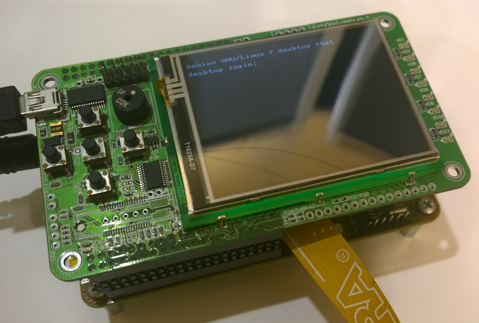
The device on which all the work was done
Documentation for writing framebuffer drivers
ILI9341 documentation
Comment on previous article
In the last article, I measured the bandwidth of the fpga2sdram interface.
Unfortunately, I made a mistake. Namely, the PLL clock was set to 125 MHz, not 25 MHz, as it really is.
Because of this, the multiplier and divider coefficients for the PLL were calculated incorrectly.
As a result, DDR3 worked at 66 MHz instead of the 333 MHz.
With the correct coefficients and interface width of 256 bits, the bandwidth is about 16-17 Gbit / s, which corresponds to the theoretical for the DDR3 interface with a width of 32 bits and a frequency of 333 MHz.
I apologize!
Small survey
I want to know the opinion of the community. If not difficult, please vote.
Source: https://habr.com/ru/post/263571/
All Articles