Reliable storage and update of data in flash memory of STM32 and MSP430 microcontrollers
Often there is the task of storing mutable data, such as configuration, in the microcontroller’s flash memory. The solution seems simple, however, to ensure the reliability of updating data, provided that the power supply can be turned off at any time, is very nontrivial, and even the use of checksums does not solve the problem completely. From this article you will learn
For those wishing to apply in practice - working code under STM32F4
The classic approach to the problem is to write data to the flash, accompanying them with checksums so that you can check the integrity of the data when reading. This approach is the basis of the scheme proposed by the author for MSP430 microcontrollers. However, it has 2 drawbacks - the complexity caused by the desire to save memory by storing data in parts that can be updated independently, and the lack of strict guarantees of data integrity during a power outage at the time of recording. By integrity we mean the following:
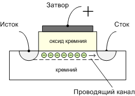
The flash memory is based on a special modification of an insulated-gate transistor (MOSFET). The classic MOSFET is formed on a silicon wafer coated with an oxide layer, which plays the role of an insulator. On top of the oxide electrode is deposited, called the gate. By applying voltage to this electrode, it is possible to control the current flowing between the two electrodes on the silicon wafer - the drain and the source. This happens because the positive charge of the gate attracts electrons and a conductive channel of electrons is formed under the gate. If you remove the voltage from the gate, the conductive channel disappears.
')
The flash memory uses floating gate transistors. They have insulated from the entire island of silicon in the thickness of the oxide between the gate and the channel. If the island is not charged, the transistor works just like a normal one. However, if we put some electrons on the island, they will compensate for the positive charge of the shutter and the channel will disappear.
Electrons fall on the floating gate in the process of recording data, tunneling through an insulator. This process is vividly shown in the film The Magicians - the main thing is to accelerate well, to see the target and not to notice obstacles. Electrons are accelerated by passing a current in the channel.
It’s harder to erase, because we don’t need to settle the electrons on the gate, but to remove them from there, it’s impossible to disperse them. Therefore, we simply form a positive potential in the channel and wait for the electrons to be attracted and tunnel through the channel. That is why erasing takes several orders of magnitude more time than writing. For our STM32, this time is from fractions of seconds to seconds. More sophisticated devices like SSD drives support some stock of erased transistors, but if they run out, the time it takes to write is dramatically increased.
To save time, erase memory with large blocks - sectors. In the case of STM32, the minimum size - 16 kilobytes - has 4 sectors located at lower addresses. Our STM32 can write one byte, two, or four. The erased transistor is read as a logical unit. Accordingly, when recording, we plant electrons on the gates of those transistors that correspond to logical zeros in the recorded data. This is an interesting observation - we can put bits in the same byte one by one, and not all at once. The reverse operation — to set the zero bit to one — is impossible without erasing. When writing a single bit, the contents of the memory does not change.
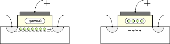
What happens if we turn off the power while data is being written? It is clear that part of the data will be recorded. And what will happen to that byte or word that we recorded at the time of power off? When writing to a floating gate can get a different number of electrons. A lot of electrons are read as 0, a little - as 1, so there is also some boundary amount of electrons. If, before turning off the power, the number of electrons close to the boundary electron reaches the gate, then when reading we can get both 0 and 1 depending on completely random factors. Over time, the charge will drain from the shutter, so the probability of reading 1 will increase. This extremely unpleasant feature makes even a scheme using a checksum unreliable. If the power is turned off at the moment of recording the last word of our data package, which we can accompany with any amount of verification information, then we can read our data today, but not tomorrow, or vice versa. Moreover, we are in trouble when we write to the area that we think is erased, because it reads like all units today, because tomorrow there may be zeros and spoil our data.
Similar problems arise when turning off the power at the time of erasing. In this case, we get a completely unpredictable memory contents with unpredictable behavior in the future. This means that such a situation needs to be able to detect and re-erase. That is why code dealing with writing to flash memory must be written in a state of heightened paranoia, and one can never say whether the degree of this paranoia is sufficient or not.
Now we are ready to consider a data storage scheme that guarantees data integrity in the sense discussed above. Since the STM does not skimp on the size of the flash, it was decided to simplify the design, refusing to save, and use a model where all the data are combined into a single structure of a fixed size. When updating data, we record the entire structure as a whole. Different versions of data are written sequentially to a previously erased flash memory area. The most recent data is considered relevant.
The system is divided into 2 levels, providing various guarantees regarding the integrity of data. At the bottom level is the data pool, which allows you to write data sequentially to a previously erased sector. Below is the format of a packet with data at this level.

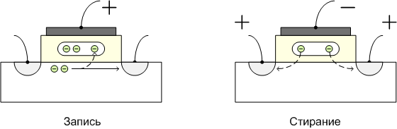
The actual data is followed by alignment to a 32 bit word, after which a checksum is written. The checksum is followed by a check byte, where we simply write the zero bits. We write this part of the data packet byte by byte, so if we see at least one zero bit in the check byte while reading, we can be sure that the checksum is written correctly and its contents will not change with time. The next byte after the check is status. There is a zero bit that marks the packet as complete. If during the reading we found this zero bit, it means that the check byte was also written correctly and its contents will not change with time. That is, we can consider the data completely recorded and our opinion will not change with time. If while reading we did not find the completion flag, but the check byte has zero bits, we simply overwrite the last 2 bytes. If, however, all single bits are read in the check byte, we assume that the data was not recorded correctly regardless of the checksum.
Why such difficulties, may ask an inquisitive reader. After all, we can simply rewrite the checksum, and it is guaranteed not to change with time. Yes, indeed, but we will have to do it every time. The goal is to
The second status bit - the continuation flag - allows you to determine whether the memory from which all units are read can be considered erased. Before writing the next block of data, we set this flag (reset the bit to 0). If while reading we see in this bit 1, then we never tried to write in the next byte. Well, what if the sector is initially empty - can we consider it erased or not? Of course not! But with this relapse of paranoia, it is easiest to cope - we will simply erase it again before writing something down.
So, we can guarantee that once read, the data will be read further. However, with the other properties of a reliable data repository, things are not so bright. There is an obvious problem with the need to periodically erase the sector when a place runs out there. If this turns off the power, we will not only not record new data, but also lose old ones. Somewhat less obvious is the problem with incorrectly recorded data (as a result of a power outage during recording). We cannot guarantee that with time the missing bits will not appear there and we will not start reading this data as correct. It may seem that additional status bits, marking the record as incorrect, may save the situation, but this is not so. After all, the power may disappear when writing these extra bits, and as a result there will only be more problems. The scheme described above successfully uses corrective entries only because they record exactly the same data as the original entry, therefore, for any power-off sequence, the last successful entry puts the flash into a stable state. Of course, in this form, the described storage can be used in applications that do not impose high demands on the reliability of storage. But it turns out that on the basis of two storages of the type described above, one can create a more reliable variant, devoid of the described disadvantages. The scheme of such storage is shown in the following figure.

Two data pools of the above type store user data (in 2 different flash sectors), supplemented by a service byte. It stores the era number and the invalid data flag (often referred to as the 'gravestone'). If the place in the current pool ends, we increase the era number by one and start writing the next one. A power outage no longer threatens to destroy all of our data, because we don’t erase the last pool of data that was recorded. The number of the pool, where the next record will occur, is equal to the least significant bit of the era number. At the start of the system, we compare the numbers of epochs (on a numerical circle) to determine the pool recorded last. The problem of stability of incomplete records is also solved quite simply. If at the start we find a record that we consider to be incorrect, then we can simply “bury” it, having made a new record with actual data, if any, or with a gravestone, if there are none.
Lies here . The project was created using the STM32CubeMX compiler under the IAR EWARM compiler for the STM32-H405 card . Using STM32CubeMX to compile the project left only positive emotions. The Klokov tree is particularly gratifying - the part that used to be a field of magic for me has now been simplified to a few mouse clicks. It is easy to adapt a project to other STM32 processors or compilers simply by regenerating it using STM32CubeMX. The data warehouse code is easy to adapt to other architectures, since working with flash is placed in a separate module with an abstract interface. The project includes an automatic data storage test, which uses a watchdog timer to reset the processor at a random point in time. In addition, the project has a test implementation of the USB CDC protocol, which simply sends back all the accepted strings. I added it because I was interested in 2 questions. First, what happens to the problems I know about in the implementation of the USB stack. It turned out that nothing - old problems are not corrected, new ones do not appear. Apparently this is the policy of the campaign - who knows about ZLP - will make himself, who does not know - will pay for support. Secondly, it was interesting how the erasing of the flash affects the operation of USB, because the processor can stop the selection of commands from the flash. It turned out that no effect.
Test project for MSP430 added to repository. It differs only in the module that implements operations with flash memory, the rest of the code is common. Tested on LaunchPad . The test cocked the timer, and the timer output was connected directly to the ground. Power to the board was fed through a 510 ohm resistor, so when the timer triggered, the power drastically subsided, and the microcontroller reseted, interrupting all current operations with flash. The test successfully completed a million flash records, which took three and a half hours. During this time, about 20,000 erasers of a 512-byte sector occurred, the power was turned off about 5,000 times. Results were checked by comparison with records in 2 separate control sectors. No errors were detected during testing.
- how does flash memory work
- what problems does the power turn off at the time of writing or erasing
- how are these problems solved
For those wishing to apply in practice - working code under STM32F4
The classic approach to the problem is to write data to the flash, accompanying them with checksums so that you can check the integrity of the data when reading. This approach is the basis of the scheme proposed by the author for MSP430 microcontrollers. However, it has 2 drawbacks - the complexity caused by the desire to save memory by storing data in parts that can be updated independently, and the lack of strict guarantees of data integrity during a power outage at the time of recording. By integrity we mean the following:
- data is either recorded or not
- the status of the operation does not change with time, i.e. if the data is recorded, they are always available, if not, then they suddenly will not appear in the future
How flash memory works
The flash memory is based on a special modification of an insulated-gate transistor (MOSFET). The classic MOSFET is formed on a silicon wafer coated with an oxide layer, which plays the role of an insulator. On top of the oxide electrode is deposited, called the gate. By applying voltage to this electrode, it is possible to control the current flowing between the two electrodes on the silicon wafer - the drain and the source. This happens because the positive charge of the gate attracts electrons and a conductive channel of electrons is formed under the gate. If you remove the voltage from the gate, the conductive channel disappears.
')
The flash memory uses floating gate transistors. They have insulated from the entire island of silicon in the thickness of the oxide between the gate and the channel. If the island is not charged, the transistor works just like a normal one. However, if we put some electrons on the island, they will compensate for the positive charge of the shutter and the channel will disappear.
Electrons fall on the floating gate in the process of recording data, tunneling through an insulator. This process is vividly shown in the film The Magicians - the main thing is to accelerate well, to see the target and not to notice obstacles. Electrons are accelerated by passing a current in the channel.
It’s harder to erase, because we don’t need to settle the electrons on the gate, but to remove them from there, it’s impossible to disperse them. Therefore, we simply form a positive potential in the channel and wait for the electrons to be attracted and tunnel through the channel. That is why erasing takes several orders of magnitude more time than writing. For our STM32, this time is from fractions of seconds to seconds. More sophisticated devices like SSD drives support some stock of erased transistors, but if they run out, the time it takes to write is dramatically increased.
To save time, erase memory with large blocks - sectors. In the case of STM32, the minimum size - 16 kilobytes - has 4 sectors located at lower addresses. Our STM32 can write one byte, two, or four. The erased transistor is read as a logical unit. Accordingly, when recording, we plant electrons on the gates of those transistors that correspond to logical zeros in the recorded data. This is an interesting observation - we can put bits in the same byte one by one, and not all at once. The reverse operation — to set the zero bit to one — is impossible without erasing. When writing a single bit, the contents of the memory does not change.
Read stability problem
What happens if we turn off the power while data is being written? It is clear that part of the data will be recorded. And what will happen to that byte or word that we recorded at the time of power off? When writing to a floating gate can get a different number of electrons. A lot of electrons are read as 0, a little - as 1, so there is also some boundary amount of electrons. If, before turning off the power, the number of electrons close to the boundary electron reaches the gate, then when reading we can get both 0 and 1 depending on completely random factors. Over time, the charge will drain from the shutter, so the probability of reading 1 will increase. This extremely unpleasant feature makes even a scheme using a checksum unreliable. If the power is turned off at the moment of recording the last word of our data package, which we can accompany with any amount of verification information, then we can read our data today, but not tomorrow, or vice versa. Moreover, we are in trouble when we write to the area that we think is erased, because it reads like all units today, because tomorrow there may be zeros and spoil our data.
Similar problems arise when turning off the power at the time of erasing. In this case, we get a completely unpredictable memory contents with unpredictable behavior in the future. This means that such a situation needs to be able to detect and re-erase. That is why code dealing with writing to flash memory must be written in a state of heightened paranoia, and one can never say whether the degree of this paranoia is sufficient or not.
Implementation with data integrity assurance
Now we are ready to consider a data storage scheme that guarantees data integrity in the sense discussed above. Since the STM does not skimp on the size of the flash, it was decided to simplify the design, refusing to save, and use a model where all the data are combined into a single structure of a fixed size. When updating data, we record the entire structure as a whole. Different versions of data are written sequentially to a previously erased flash memory area. The most recent data is considered relevant.
The system is divided into 2 levels, providing various guarantees regarding the integrity of data. At the bottom level is the data pool, which allows you to write data sequentially to a previously erased sector. Below is the format of a packet with data at this level.
The actual data is followed by alignment to a 32 bit word, after which a checksum is written. The checksum is followed by a check byte, where we simply write the zero bits. We write this part of the data packet byte by byte, so if we see at least one zero bit in the check byte while reading, we can be sure that the checksum is written correctly and its contents will not change with time. The next byte after the check is status. There is a zero bit that marks the packet as complete. If during the reading we found this zero bit, it means that the check byte was also written correctly and its contents will not change with time. That is, we can consider the data completely recorded and our opinion will not change with time. If while reading we did not find the completion flag, but the check byte has zero bits, we simply overwrite the last 2 bytes. If, however, all single bits are read in the check byte, we assume that the data was not recorded correctly regardless of the checksum.
Why such difficulties, may ask an inquisitive reader. After all, we can simply rewrite the checksum, and it is guaranteed not to change with time. Yes, indeed, but we will have to do it every time. The goal is to
- Do not make extra entries
- To be able to understand why the checksum does not match. If the check byte is correct, then the checksum mismatch unambiguously indicates that the contents of the sector are damaged or not completely erased.
The second status bit - the continuation flag - allows you to determine whether the memory from which all units are read can be considered erased. Before writing the next block of data, we set this flag (reset the bit to 0). If while reading we see in this bit 1, then we never tried to write in the next byte. Well, what if the sector is initially empty - can we consider it erased or not? Of course not! But with this relapse of paranoia, it is easiest to cope - we will simply erase it again before writing something down.
So, we can guarantee that once read, the data will be read further. However, with the other properties of a reliable data repository, things are not so bright. There is an obvious problem with the need to periodically erase the sector when a place runs out there. If this turns off the power, we will not only not record new data, but also lose old ones. Somewhat less obvious is the problem with incorrectly recorded data (as a result of a power outage during recording). We cannot guarantee that with time the missing bits will not appear there and we will not start reading this data as correct. It may seem that additional status bits, marking the record as incorrect, may save the situation, but this is not so. After all, the power may disappear when writing these extra bits, and as a result there will only be more problems. The scheme described above successfully uses corrective entries only because they record exactly the same data as the original entry, therefore, for any power-off sequence, the last successful entry puts the flash into a stable state. Of course, in this form, the described storage can be used in applications that do not impose high demands on the reliability of storage. But it turns out that on the basis of two storages of the type described above, one can create a more reliable variant, devoid of the described disadvantages. The scheme of such storage is shown in the following figure.
Two data pools of the above type store user data (in 2 different flash sectors), supplemented by a service byte. It stores the era number and the invalid data flag (often referred to as the 'gravestone'). If the place in the current pool ends, we increase the era number by one and start writing the next one. A power outage no longer threatens to destroy all of our data, because we don’t erase the last pool of data that was recorded. The number of the pool, where the next record will occur, is equal to the least significant bit of the era number. At the start of the system, we compare the numbers of epochs (on a numerical circle) to determine the pool recorded last. The problem of stability of incomplete records is also solved quite simply. If at the start we find a record that we consider to be incorrect, then we can simply “bury” it, having made a new record with actual data, if any, or with a gravestone, if there are none.
Test project
Lies here . The project was created using the STM32CubeMX compiler under the IAR EWARM compiler for the STM32-H405 card . Using STM32CubeMX to compile the project left only positive emotions. The Klokov tree is particularly gratifying - the part that used to be a field of magic for me has now been simplified to a few mouse clicks. It is easy to adapt a project to other STM32 processors or compilers simply by regenerating it using STM32CubeMX. The data warehouse code is easy to adapt to other architectures, since working with flash is placed in a separate module with an abstract interface. The project includes an automatic data storage test, which uses a watchdog timer to reset the processor at a random point in time. In addition, the project has a test implementation of the USB CDC protocol, which simply sends back all the accepted strings. I added it because I was interested in 2 questions. First, what happens to the problems I know about in the implementation of the USB stack. It turned out that nothing - old problems are not corrected, new ones do not appear. Apparently this is the policy of the campaign - who knows about ZLP - will make himself, who does not know - will pay for support. Secondly, it was interesting how the erasing of the flash affects the operation of USB, because the processor can stop the selection of commands from the flash. It turned out that no effect.
Update - option for MSP430
Test project for MSP430 added to repository. It differs only in the module that implements operations with flash memory, the rest of the code is common. Tested on LaunchPad . The test cocked the timer, and the timer output was connected directly to the ground. Power to the board was fed through a 510 ohm resistor, so when the timer triggered, the power drastically subsided, and the microcontroller reseted, interrupting all current operations with flash. The test successfully completed a million flash records, which took three and a half hours. During this time, about 20,000 erasers of a 512-byte sector occurred, the power was turned off about 5,000 times. Results were checked by comparison with records in 2 separate control sectors. No errors were detected during testing.
Source: https://habr.com/ru/post/262163/
All Articles