Functional DDS generator on the FPGA
 Recently, I saw a signal generator project on an AVR microcontroller. The principle of generation is DDS , based on the Jesper library, the maximum frequency is 65534 Hz (and up to 8 MHz HS output with a square wave). And then I thought that the generator is an excellent task, where the FPGA can show itself in the best possible way. As a sports interest, I decided to repeat the project on the FPGA, while meeting the deadlines on two days off, and the parameters to get are not strictly defined, but the maximum possible. What came out of this can be found under the cut
Day zero
 Before the weekend came, I had a little time to think about the implementation. To simplify my task, I decided to make the generator not as a separate device with buttons and an LCD screen, but as a device that connects to a PC via USB. For this, I have a USB2RS232 board . The driver board does not require (CDC), so I think it will work under Linux (for some, this is important). Also, I will not hide that I already worked with the reception of messages on RS232. I will take modules for work with RS232 ready with opencores.com .
To generate a sinusoidal signal, you will need a DAC. I chose the type of DAC, as in the initial project - R2R on 8 bits. It will allow to work at high frequencies, of the order of megahertz. I am convinced that the FPGA must cope with this
 About what to write a program for data transmission through the COM port, I was thinking. On the one hand, you can write on Delphi7, the experience of writing such a program already exists, besides, the size of the executable file will not be large. I also tried to sketch something to work with Serial in the form of a java script in the html page, but more or less earned only through the Chrome serial API, but for this you need to install the plugin ... in general, too, disappears. As an innovation, I tried PyQt5 for myself, but when distributing such a project, you need to drag a bunch of libraries. Having tried to build a PyQt project in an exe file, it turned out more than 10 MB. That is, there will be nothing better than an application written in c ++ \ Qt5. I should also take into account that I don’t have any development experience in python, but I do have Qt5. Therefore, the choice fell on Qt5. From the fifth version there appeared a module for working with serial and I already worked with it. And the application on Qt5 can be transferred to Linux and Mac (for some, this is important), and from version 5.2, applications on QWidgets can be transferred even to a smartphone!
What else is needed? Naturally board with FPGA. I have two of them (Cyclone iv EP4CE10E22C8N for 10 thousand cells, and Cyclone ii EP2C5 for 5 thousand cells). I will choose the one on the left, solely because of the more convenient connector. In terms of volume, the project does not intend to be large, so it fits in either of the two. In terms of speed, they do not differ. Both boards have “on board” 50 MHz generators, and inside the FPGA there is a PLL , with which I can increase the frequency to the planned 200 MHz.
')

The first day
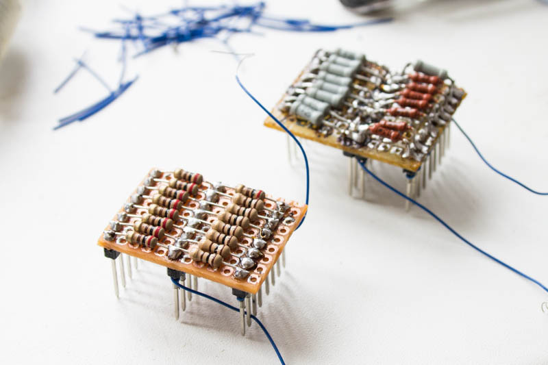
Due to the fact that I already did the DDS module in my synthesizer project, I immediately took up the soldering iron and began to solder the DAC on the resistors. He took a mockup. Installation did with the use of cheating . The only change that affected the technology was that I abandoned the acid F38N for tinning the racks in favor of the TT indicator flux gel . The essence of the technology is simple: I solder racks to the PCB, solder resistors on them from the PCB side. Missing connections are performed by wrap. Still, the racks are convenient because I can insert them directly into the FPGA board.
Unfortunately, at home there were no resistors 1 and 2 kilooma. There was no time to go to the store. I had to sacrifice one of their rules, and remove the resistors from the old unnecessary board. They used resistors 15K and 30K. The result is such a Frankenstein:

Then I launched Quartus, created a project.
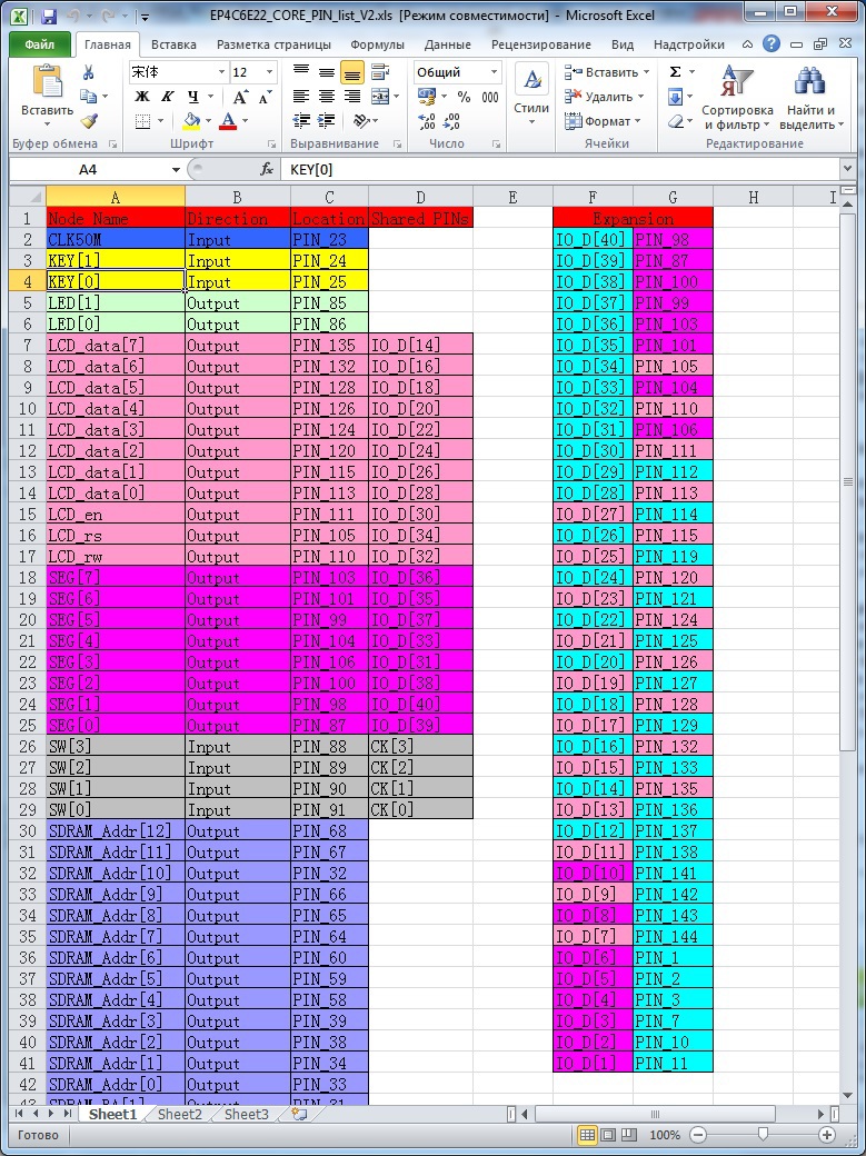
After creating the project, you need to set the target device: Assigments menu -> Device

Further, in the same place I press the button “Device and Pin options” because some pins are configured so that they will not work. I configure everything as "Use as regular I / O"

Further, in the same place I press the button “Device and Pin options” because some pins are configured so that they will not work. I configure everything as "Use as regular I / O"
In the project, I "nahadrkodil" unmanaged main module DDS at a fixed frequency.
1000 Hz Generator Module
module signal_generator(clk50M, signal_out); input wire clk50M; output wire [7:0] signal_out; wire clk200M; osc osc_200M reg [31:0] accumulator; assign signal_out = accumulator[31:31-7]; // 1000 //50 000 000 Hz - //2^32 = 4 294 967 296 - DDS - 32 // 1000Hz / 50 000 000 Hz / 2 * 4294967296 => 42949,67296 always @(posedge clk50M) begin accumulator <= accumulator + 32'd42949; end endmodule After that, I clicked “Start Compilation” so that the development environment wondered what our input / output lines are in the main project module and what physical PIN's they are connected to. You can connect to almost any. After compilation, assign the appeared lines to the real PIN of the FPGA chip:
Assigments menu item -> Pin Planner
On the HS_OUT, key0 and key1 lines, I ask you not to pay attention yet, they appear in the project afterwards, but I didn’t manage to make the screen at the very beginning.

In principle, it is enough to “register” only PIN_nn in the Location column, and the remaining parameters (I / O standart, Current Strench and Slew Rate) can be left by default, or you can choose the same options that are suggested by default (default) so that there is no warning 's.
In principle, it is enough to “register” only PIN_nn in the Location column, and the remaining parameters (I / O standart, Current Strench and Slew Rate) can be left by default, or you can choose the same options that are suggested by default (default) so that there is no warning 's.
How to find out what PIN corresponds to the slot number on the board?
Socket pin numbers are on board

And the FPGA pins, to which the connector pins are connected, are described in the documentation that comes with the FPGA board.
And the FPGA pins, to which the connector pins are connected, are described in the documentation that comes with the FPGA board.
After the pins are assigned, I compile the project again and flash it with the help of a USB programmer. If the drivers for the USB Byte blaster programmer are not installed, then indicate to Windows that they are located in the folder where you installed Quartus. Then she will find herself.
Connect the programmer to the JTAG connector. A menu item for programming "Tools -> Programmer" (or click the icon on the toolbar). The “Start” button, joyful “Success” and the firmware are already inside the FPGA and are already working. Just do not turn off the FPGA, otherwise she will forget everything.
Tools -> Programmer
The DAC is connected to the FPGA board connector. I connect the oscilloscope S1-112A to the DAC output. As a result, the “saw” should turn out because the high bit of the word DDS of the battery of the phase is output on 8 bits. And it always increases until it overflows.
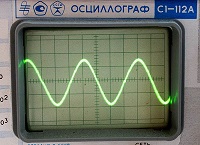
Some 1.5 hours and for a frequency of 1000 Hz, I see the following waveform:

I want to note that the "saw" in the middle has a small fracture. It is due to the fact that the resistors have a spread of values.
Another important point that needed to be clarified is the maximum possible frequency with which the DDS generator will work. With correctly configured TimeQuest parameters, after compilation in the Compilation Report, you can see that the speed of the circuit is above 200 MHz with a margin. And this means that I will multiply the frequency of the 50 MHz oscillator with the help of PLL by 4. I will increase the value of the battery of the DDS phase with a frequency of 200 MHz. The final frequency range that can be obtained in our conditions is 0 - 100 MHz. Frequency setting accuracy:
200 000 000 (clk) / 2^32 (DDS) = 0,047 That is, it is better than ~ 0.05 Hz. I consider the accuracy in the Hertz fraction for a generator with such a range of operating frequencies (0 ... 100 MHz) to be sufficient. If someone needs to increase accuracy, then for this you can increase the DDS bit (do not forget to check the TimeQuest Timing Analyzer, that the speed of the logic is within CLK = 200 MHz, because it is an accumulator), or simply reduce the clock frequency, if such A wide range of frequencies is required.
TimeQuest Timing Analyzer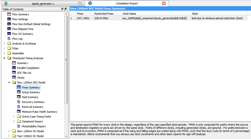
After I saw the “saw” on the screen, family matters forced me to go to the country (the same day off). There I mowed, cooked, grilled kebabs and did not know about the surprise that I was waiting for in the evening. Already closer to the night before bedtime, I decided to look at the waveform for other frequencies.
For a frequency of 100 kHz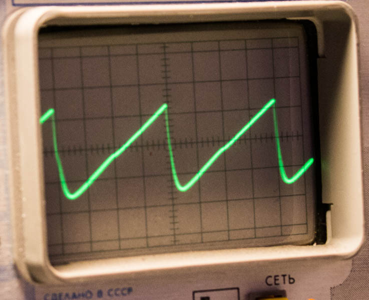
For a frequency of 250 kHz
For the frequency of 500 KHz
For frequency 1 MHz
I will not hide that the shape of the signals has upset me, especially at 1 MHz (pathetic, useless megahertz!). I planned to get the frequencies of several other orders. After reading about the R2R DAC, the cause of the problem became clear - stray capacitances. Therefore, the plans for the next day, it was decided to make a DAC on 100 and 200 Ohm resistors, which I have in stock, and leave this DAC for future developments that do not require working at such high frequencies, because the smoothness of the saw also has its plus.
Second day
Due to the fact that it was interesting how the DAC will work on resistors of 100 and 200 Ohms, I immediately took up the soldering iron. This time, the DAC turned out to be more accurate, and it took less time to assemble it.
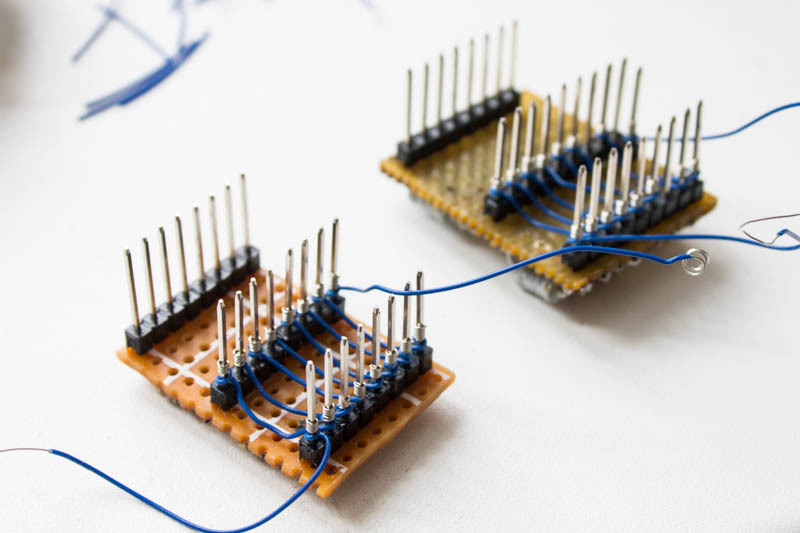
We put the DAC on the FPGA board and connect it to the oscilloscope

Checking 1 MHz - IN! It is quite another matter!

Saw 10 MHz
Saw 25 MHz
The shape of the saw at 10 MHz is still similar to the correct one. But at 25 MHz, it is already quite "not beautiful." However, C1-112a has a bandwidth of 10 MHz, so in this case the reason may already be in the oscilloscope.
In principle, this issue with the DAC can be considered closed. Now remove the high-speed waveform. To do this, we will output the most significant bit to a separate PIN FPGA. The data for this line will be taken from the high bit of the DDS battery.
assign hs_out = accumulator[31]; 1 MHz square wave
5 MHz meander
Meander 25 MHz
50 MHz meander is almost not visible
But I think that the output of the FPGA would be worth the load on the resistance. Perhaps the fronts would be cooler.
Sine is done on the table. The size of the table is 256 values of 8 bits each. It would be possible to take more, but I already had a ready mif file. Using the wizard, create a ROM element with the sine table data from the mif file.
Creating a ROM - Tools -> Mega Wizard Plugin manager
Select 1 port ROM and set the name for the module.

Agree

Here we also agree
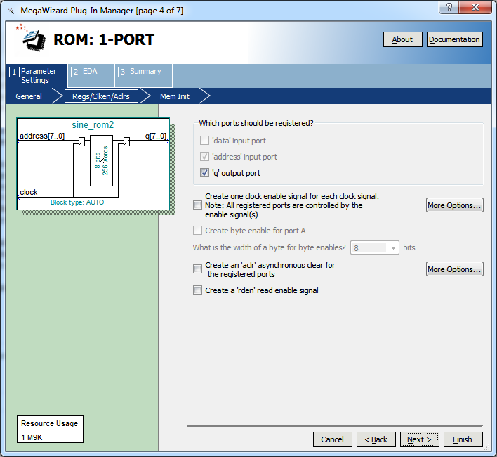
Using browse we find our mif file with sine table

Here, too, do not change anything

We uncheck the sine_rom_bb.v module - it is not needed. Next finish. Quartus will ask you to add a module to the project - we agree. After that, the module can be used just like any other module in Verilog.

Select 1 port ROM and set the name for the module.
Agree
Here we also agree
Using browse we find our mif file with sine table
Here, too, do not change anything
We uncheck the sine_rom_bb.v module - it is not needed. Next finish. Quartus will ask you to add a module to the project - we agree. After that, the module can be used just like any other module in Verilog.
The upper 8 bits of the DDS battery word will be used as the ROM address, and the data output will be the sine value.
Code
//sine rom wire [7:0] sine_out; sine_rom sine1(.clock(clk200M), .address(accumulator[31:31-7]), .q(sine_out)); The sine waveform at different frequencies looks ... the same.

If desired, you can consider the problems of the DAC associated with the scatter of resistors:

Well, this weekend is over. But not yet written software for PC control. I am compelled to state the fact that I did not meet the planned deadlines.
Third day
There is very little time, so we are writing a program in haste (in the best traditions). In some places, in order to reduce the number of letters and the convenience of entering information from the keyboard, an event filter by the name of the widget is used. Please understand and forgive.
Interface

GitHub source code. There is also an application already compiled under windows.
The code is as simple as 5 kopecks. Among other things, you need to add the serialport module to the project file.
QT += core gui serialport Opening COM port
QSerialPort serial; ... serial.setPortName(ui->lbSerialPortInfo->currentText()); serial.setBaudRate(QSerialPort::Baud115200); serial.setDataBits(QSerialPort::Data8); serial.setParity(QSerialPort::NoParity); serial.setStopBits(QSerialPort::OneStop); serial.setFlowControl(QSerialPort::NoFlowControl); serial.open(QIODevice::ReadWrite); Forming and sending a message
QByteArray source; QDataStream stream(&source, QIODevice::ReadWrite); stream << (qint8)(01); // set freq msg stream << waveform; stream << adder32; serial.write(source); Day four
In a hurry, we finish receiving data on the UART. To receive messages on the UART you need to put a couple of modules. One Baud generator, the second - the receiver. In order for the receiver to work at 115200, you need to make some calculations, assuming that the main clock frequency is 200 MHz.
Baud_gen module
parameter global_clock_freq = 200000000; parameter baud_rate = 115200; // - UART // first register: // baud_freq = 16*baud_rate / gcd(global_clock_freq, 16*baud_rate) //Greatest Common Divisor - . http://www.alcula.com/calculators/math/gcd/ // second register: // baud_limit = (global_clock_freq / gcd(global_clock_freq, 16*baud_rate)) - baud_freq // parameter GCD = (baud_rate==115200) ? 12800 : 0; parameter baud_freq = 16*baud_rate / GCD; parameter baud_limit = (global_clock_freq / GCD) - baud_freq; wire uart_clk; baud_gen BG(.clock(clk), .reset(rst), .ce_16(uart_clk), .baud_freq(baud_freq), .baud_limit(baud_limit)); I put the message receiving module, uart_clk is sent to it and the signal is from the physical input of the FPGA.
Uart_rx module
//RCV wire [7:0] uart_command; wire uart_data_ready; uart_rx URX(.clock(clk), .reset(rst), .ce_16(uart_clk), .ser_in(rx), .rx_data(uart_command), .new_rx_data(uart_data_ready) ); Then I put all this in a separate module, which gives only the number of the waveform and the increment value to the register of the battery of the DDS phase.
Ctrl.v module
module ctrl(clk, rst, rx, wf, adder); input wire clk, rst, rx; output wire [7:0] wf; //wave form output wire [31:0] adder;// adder value reg [7:0] wf_reg; initial wf_reg <= 8'd0; reg [31:0] adder_reg; initial adder_reg <= 32'd1073741; When the uart_rx module received a byte of information, it puts the uart_data_ready line into one unit. At this time on the line uart_command is received bytes. To receive a message I am writing a steytmashin.
State machine
//rcv state machine parameter SM_READY = 4'd0; parameter SM_FRQ_WF = 4'd1; parameter SM_FRQ_DDS1 = 4'd2; parameter SM_FRQ_DDS2 = 4'd3; parameter SM_FRQ_DDS3 = 4'd4; parameter SM_FRQ_DDS4 = 4'd5; //messages parameter CMD_SETFREQ = 8'd1; reg [3:0] rcv_state; initial rcv_state <= SM_READY; always @ (posedge clk) begin if (uart_data_ready==1) begin if (rcv_state==SM_READY) begin rcv_state = (uart_command==CMD_SETFREQ) ? SM_FRQ_WF : rcv_state; end else if (rcv_state==SM_FRQ_WF) begin wf_reg <= uart_command; rcv_state <= rcv_state + 1'b1; end else if (rcv_state==SM_FRQ_DDS1) begin adder_reg <= (adder_reg << 8) + uart_command; rcv_state <= rcv_state + 1'b1; end else if (rcv_state==SM_FRQ_DDS2) begin adder_reg <= (adder_reg << 8) + uart_command; rcv_state <= rcv_state + 1'b1; end else if (rcv_state==SM_FRQ_DDS3) begin adder_reg <= (adder_reg << 8) + uart_command; rcv_state <= rcv_state + 1'b1; end else if (rcv_state==SM_FRQ_DDS4) begin adder_reg <= (adder_reg << 8) + uart_command; rcv_state <= SM_READY; end else begin rcv_state <= SM_READY; end end //ucom_ready end Output data to the outputs of the module
Conclusion
assign adder = adder_reg; assign wf = wf_reg; Add the receiving module to the main module.
Add ctrl module to the main module
//rs232 rcvr wire [31:0] adder_value; wire [7:0] waveform; ctrl ctrl_0(.clk(clk200M), .rst(rst), .rx(RS232in), .wf(waveform), .adder(adder_value)); Increment value added to the battery phase
Increase the value of the battery with each beat
always @(posedge clk200M) begin accumulator <= accumulator + adder_value; end From the highest part of the value of the battery phase, we obtain the remaining waveforms. And depending on the selected form - connect it to the output.
Waveforms
// wave_forms parameter SINE = 8'd0; parameter SAW = 8'd1; parameter RAMP = 8'd2; parameter TRIA = 8'd3; parameter SQUARE = 8'd4; parameter SAWTRI = 8'd5; parameter NOISE = 8'd6; wire [7:0] saw_out = accumulator[31:31-7]; wire [7:0] noise_out = 8'd127; //! wire [7:0] ramp_out = -saw_out; wire [7:0] square_out = (saw_out > 127) ? 8'b11111111 : 1'b00000000; wire [7:0] saw_tri_out = (saw_out > 7'd127) ? -saw_out : 8'd127 + saw_out; wire [7:0] tri_out = (saw_out>8'd191) ? 7'd127 + ((saw_out << 1) - 9'd511) : (saw_out>8'd063) ? 8'd255 - ((saw_out << 1) - 7'd127) : 7'd127 + (saw_out << 1); //sine rom wire [7:0] sine_out; sine_rom sine1(.clock(clk200M), .address(saw_out), .q(sine_out)); wire [7:0] signal = (waveform == SINE) ? sine_out : (waveform == SAW) ? saw_out : (waveform == RAMP) ? ramp_out : (waveform == TRIA) ? tri_out : (waveform == SQUARE) ? square_out : (waveform == SAWTRI) ? saw_tri_out : (waveform == NOISE) ? noise_out : 8'd127; //TODO I was almost not surprised that it immediately worked. The only mistake I found was in the calculations: I divided the desired frequency into CLK, then by two more, then multiplied by the battery capacity. But this is not necessary, because we get 1 period when the value of the battery changes from 0 to MAX. It is necessary to divide an additional 2 only if taking the most significant bit of the battery frequency as the output of the meander (in this case the frequency is 2 times lower). But getting the meander I redid.
Day four
It can include the time spent on each day in the design of the article.
We proceed to check. First with an oscilloscope.
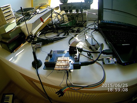
At radio frequencies from 28 to 100 MHz, I decided to listen to the generator using an SDR receiver, placing the antenna next to the board.

findings
As is often the case in IT, there was an error of 2–2.5 times with the time estimate. The goal has been achieved: a generator up to 100 MHz is assembled on the knee. However, so that this work could be called a full-fledged generator, it will take more work. Therefore, there are great prospects for development. Due to the deadlines, I did not add what I could in principle: 1) a noise generator; 2) a wave generator that the user draws himself; 3) digital sequence generator. There is no amplitude and offset adjustment in the generator.
227 cells out of 10,000 were used. A list of what else can be added to the project:
- Expand the bit width of the DAC
- Increase the number of outputs with generated signals
- Apply the DAC chip in a higher bit depth
- Implement amplitude and offset control
- Add controls, LCD screen, for portability
- Add noise generator and other simple waveforms
- Add the ability to download arbitrary waveforms
I think that anyone can do this on their own by expanding the project with the necessary functionality. Add is easier than from scratch. The format of the control command is very simple, so the generator can be controlled from a microcontroller.
Source codes: https://github.com/UA3MQJ/fpga-signal-generator
Links with analogues
Far from complete list
Functional DDS generator. Created database AVR. Frequencies 0 ... 65534 Hz.
Overview of the DDS-generator GK101. Created using FPGA Altera MAX240. Frequencies up to 10 MHz.
Multifunctional generator on the PIC16F870. Frequency range: 11 Hz - 60 kHz.
Analog function generator. Frequency range ranges from 20 Hz to 300 kHz.
USB function generator on AD9833. Based on the DDS chip.
Mini DDS is the simplest transmitter for the 137 kHz range and not only. The frequency is 136 kHz.
DDS is a functional generator with “jumper” control on the PLA.
Source: https://habr.com/ru/post/260999/
All Articles