Making homemade accessories for Dendy
At first I did not even think of writing an article on this topic, but it seems that this is already part of a whole series of articles on Dandy topics. And yes, this time it is primarily about the domestic Dandy, and not about the original console - Famicom or NES. I just made the device as a gift to one person who shoots very interesting videos about Dandy, and focused on compatibility with this particular clone.
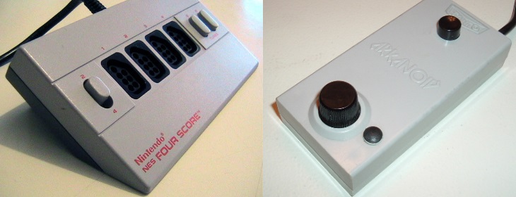
The fact is that for Famicom and for NES there were a variety of accessories: 3D glasses, keyboards, robots, barcode readers, all sorts of game controllers, and much more . Only the light gun reached us. I had the task to assemble a device that would combine a splitter into four players (yes, there were such games) and an Arkanoid-controller.
')
First of all, it’s worth telling how the Famicom, NES and Dendy game controllers work withjoysticks , and how they differ in this regard.
From the point of view of games, I / O ports are two registers with addresses $ 4016 and $ 4017 , which are associated respectively with two ports, where everything is connected. But on standard controllers for reading data only one wire is used - D0 , the data from which are available, respectively, through the low (zero) bit in each of the registers: $ 4016.0 and $ 4017.0 . Similarly, one wire is used for recording, it is usually called STROBE (or LATCH ), which resets the counter inside the gamepad, and which is available through an entry of $ 4016.0 (yes, it is common for both controllers).
Simply put, to get the status of the buttons on the first controller, you must first write 1 to $ 4016.0 , immediately write 0 to it, dropping the counter, and then read $ 4016 and $ 4017 eight times (for each of the buttons), getting data on the buttons from the lower bit But why are the other bits in these registers, where do these lines go? Consider the controller port at NES:
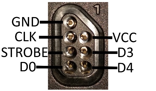
Yes, D3 and D4 actually go to him! It is they that are available through $ 4016.3 , $ 4016.4 at the first port and $ 4017.3 , $ 4017.4 at the second, and they are used for non-standard controllers.
As for his Japanese brother, Famicom, these ports are not there, and the game controllers themselves are not disconnected from the console, but it has an expansion port, which is a DB-15 connector.
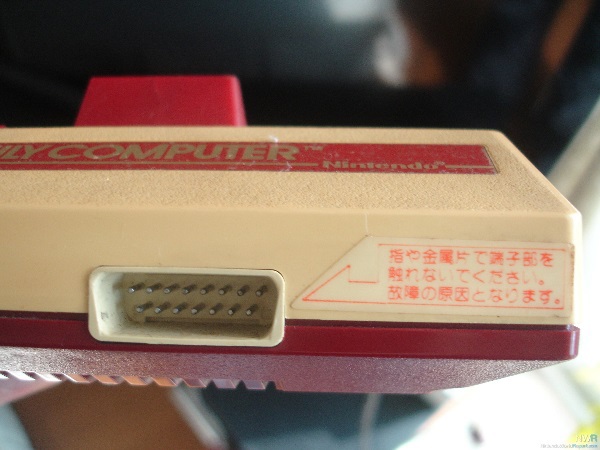
Familiar looks, right? Yes, when the Chinese designed our Dandy (I doubt that it was designed by us), and they had to make the disconnecting controllers, they decided to use the expansion port as a basis, because it has contacts for the second controller, and it is located on Famicom right of center. They do not even have to change the pinout here. As for the first controller, they took the same DB-15, positioned it on the left and swapped the pinout so that the first controller could be connected. And only him.
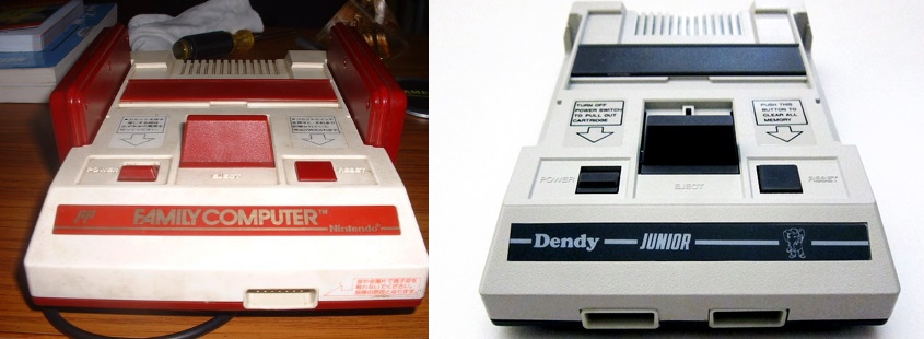
Compare the front ports themselves at Famicom and our Dandy:
Here is such a strange story of these fifteen-pin connectors from gamepads that are used in our country.
But let's see what is brought to this expansion port from Famicom?
(screenshot from wiki.nesdev.com )
Yes, another $ 4016.1 (on input), $ 4017.0-4 (on input), $ 4017.0-2 (on output), external interruption and even sound go to it I was very pleasantly surprised when I disassembled the Dandy and saw that all this is there:
True, not all models, as it turned out. But if it is, it means there is full compatibility with accessories for Famicom, and the corresponding Japanese games can use them. But let me remind you that Dandy is a very strange mixture of NES and Famicom, PAL and NTSC. The pirates produced for her both Japanese and American games, which are essentially 100% compatible, if you do not take into account these accessories and different cartridge formats.
Total: in some Dandies there are all the same conclusions as on the Famikom, which at the same time include some of the conclusions available on the NES. There is no access to $ 4016.3 and $ 4016.4 , but they are rarely used. In the form of tablets for clarity:
The American four-player splitter for the NES called the Four Score is a simple set of shift registers. Those. the first eight reads from $ 4016.0 give data from the first controller, and the second eight from the third. Similarly, $ 4017.0 gives data on the second and fourth controllers. In addition, when you continue reading, the device issues its signature, with which the game determines that it is the Four Score that is connected, and not something else. It turns out that such a device can be assembled from six shift registers (4021 or 74165), and it will work on any Dandy, because it does not require additional data lines. Of course, only with the American games that came out for the NES.
The Japanese counterpart for Famicom is much simpler. The third and fourth controllers are connected directly to the expansion port and are available through $ 4016.1 and $ 4017.1 . Accordingly, for such an adapter, we already need a full-fledged expansion port at the Dandy, otherwise the four of us will not be able to play Japanese games.
The Arkanoid controller, as the name implies, is used to play Arkanoid and is a twist-knob and one button. Inside it is an analog-to-digital converter and a shift register, which also consistently gives the position of the handle. The difference between the Japanese and American versions is only in the connection method. The Japanese version of the game reads the position of the knob and the state of the button from $ 4016.1 and $ 4017.1 , and the American version from $ 4016.3 and $ 4016.4, respectively. It turns out that for the Japanese Arkanoid you need a full-fledged expansion port, and for the American any dandy is suitable where the light gun works (it uses the same conclusions).
Although the above devices themselves have a simple scheme and are assembled from the simplest logical components, for the heart of an all-in-one device I decided to use FPGAs. Moreover, I wished to make a simple switch switch there, but I wanted to make it possible to switch buttons A and B. First, I chose Altera EPM3064ATC100 , but it soon became clear that 64 macro cells were not enough for me, and the choice fell on EPM3128ATC100 , where there are already 128 macrocells.
If it comes to that, I decided not to have a trifle at all and put some kind of screen into the device, which would display the current mode and menu with settings, besides, I have had one sign for the synthesis of the “16x2” display for a long time. I already need a microcontroller to work with it, and I chose ATMEGA16 .
It has always been the hardest thing for me to give a device a nice look. Still, I am a programmer, not a designer, but it was during the manufacture of the device as a gift I wanted to make it as beautiful and convenient as possible. Moreover, this is almost the only way to somehow show others your work of art: photos and videos are not something, according to ready-made schemes and 3D models such things recreate units, mass production is difficult to set up, but a gift is the very thing.
So, the appearance requirements were as follows: four ports for standard DB-15 controllers from Dandy, four buttons for selecting and configuring them, a “mode” button, a “settings” button, a convenient handle for Arkanoid and a button for it that should to settle down conveniently and not to interfere. In addition, I wanted to make the active ports illuminate with LEDs and somehow intuitively communicate with the corresponding buttons, it’s most logical to arrange the connectors in a row, but these stupid DB-15s are too huge for that. In addition to all the device should be comfortable in the hands, because it is in itself a game controller for Arkanoid. In the end, I came to something like this:
Buttons in a row, ports on top of each other, handle on the side, button for Arkanoid back left.
It turns out that there is a lot of space inside. Therefore, I decided to carry out the FPGA with connectors for wires and nests to one board, and a microcontroller with a screen and buttons to another. They are connected with the simplest serial interface.
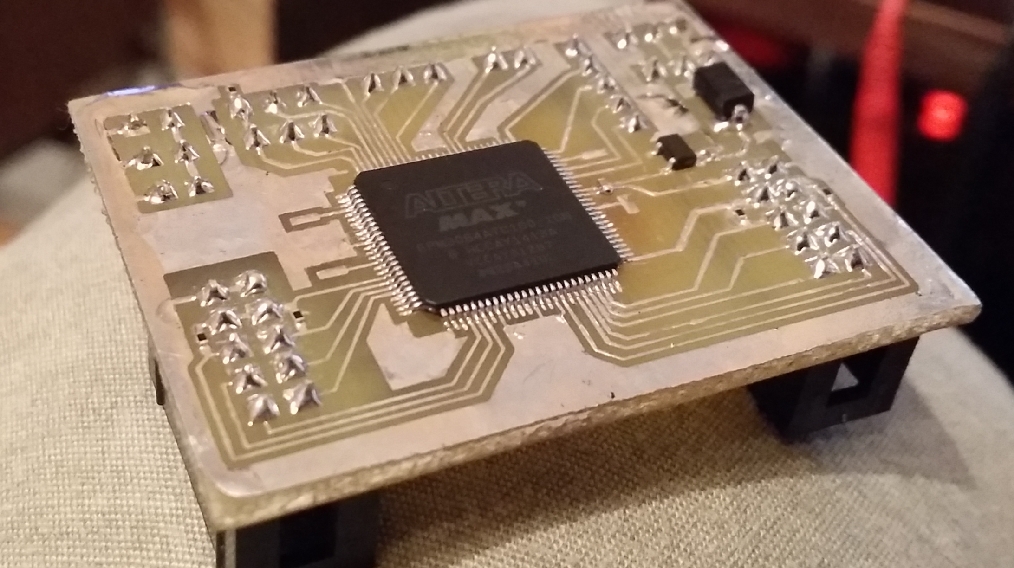
Board with FPGA (first version):
The second board:

I wrote the code for FPGAs on Verilog. For each mode, it turns out quite simple. First of all, for many of them, we need to consider calls to each of the ports, i.e. impulses on wire clock:
(sorry, habr doesn't know how to highlight Verilog)
Where strobe_in is strobe (one on both ports), and clock1_in and clock2_in are respectively clock on each of the ports. Inside the console there is a logic: clock = R / W nand (address == $ 4016 / $ 4017), i.e. on clock is a logical zero when the console reads the data at the corresponding address.
The imitation mode of the American splitter for four players looks like this:
In the mode of a Japanese splitter for four, you just need to connect the inputs to the outputs directly:
The most difficult thing was to make it possible to swap buttons A and B, because they are read sequentially, that is, you need to know in advance the value of B when the console requests A, but it is issued just after A. At first, I thought to somehow speedily read data from the controller using some external clock generator, but in the end I decided to just take the value from the previous read . This gives a delay, but it is completely invisible. Moreover, games usually read the state of the buttons several times in a row.
Of course, all these modes and settings must somehow be set. To do this, I defined a 12-bit control register, which is written to it via a serial connection, with an additional parity bit:
Accordingly, from the side of the microcontroller, the code (very dirty) looks like this:
The rest of the microcontroller code is nothing special: working with the display on the HD44780 controller, buttons, LEDs, a simple menu and working with the analog-to-digital converter to determine the angle of rotation of the handle.
I debugged everything, I was convinced of working capacity and I already started stuffing the components into the case ...

But before closing the lid I decided to check on the original Famicom, because the device will also be used with it. Alas, the modes where it was necessary to count clock pulses did not work correctly. With the help of a logic analyzer, it turned out that the data line leads to a clock line:
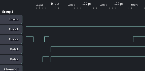
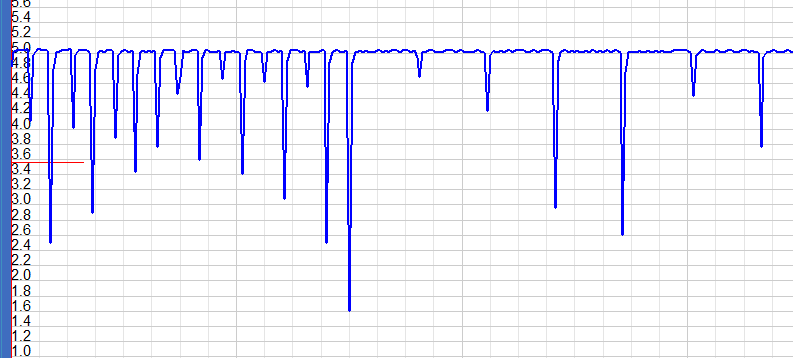
This is a noise of only a few tens of nanoseconds that spoils everything. I decided to see with my simple oscilloscope what happens on the Dandy clock line:
And here that in the same at Famikom:
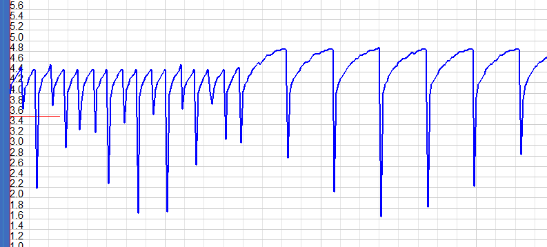
It can be seen that this line is pulled to VCC, with what is very strong in Dandy and very weak in the original Famikom. I started experimenting with the kit. It soon became clear that it was better to look at the result not with a logical analyzer, but with the console itself. I had to remember the assembler for the 6502 processor, write a simple program for testing and write it to the cartridge:
It immediately became clearly visible, and at the same time it was possible to test all modes at once, without changing the game. ROM can be downloaded here .
As a result, the problem was solved by tightening the clock lines to the VCC through a 1 kOhm resistor, a capacitor between the clock and the ground at 22nF, and 200 ohm resistors into the break of all data lines. Alas, I had to poison a new board (I did not photograph it), but after that everything immediately worked.
The final view of the device:

In Soviet times, I could be a good industrial designer.
Many probably will want to see the video, but at the moment the gift is already in the hands of our mail, and I shot only a small video instruction for the end user. You can see it here: www.youtube.com/watch?v=39beci7nE8w
And if you are interested in the themes of the work of various game controllers and the creation of self-made ones, we just shot the second series of our show “While everyone is playing” on this topic, where a lot is very simply and clearly explained to those who are not at all in the subject:
http://www.youtube.com/watch?v=nG-QznTyQKA
Information on the architecture of these consoles and accessories was taken from the site wiki.nesdev.com
Full code for FPGAs on Verilog: pastebin.com/nt39ZGvH
The fact is that for Famicom and for NES there were a variety of accessories: 3D glasses, keyboards, robots, barcode readers, all sorts of game controllers, and much more . Only the light gun reached us. I had the task to assemble a device that would combine a splitter into four players (yes, there were such games) and an Arkanoid-controller.
')
I / O ports
First of all, it’s worth telling how the Famicom, NES and Dendy game controllers work with
From the point of view of games, I / O ports are two registers with addresses $ 4016 and $ 4017 , which are associated respectively with two ports, where everything is connected. But on standard controllers for reading data only one wire is used - D0 , the data from which are available, respectively, through the low (zero) bit in each of the registers: $ 4016.0 and $ 4017.0 . Similarly, one wire is used for recording, it is usually called STROBE (or LATCH ), which resets the counter inside the gamepad, and which is available through an entry of $ 4016.0 (yes, it is common for both controllers).
Simply put, to get the status of the buttons on the first controller, you must first write 1 to $ 4016.0 , immediately write 0 to it, dropping the counter, and then read $ 4016 and $ 4017 eight times (for each of the buttons), getting data on the buttons from the lower bit But why are the other bits in these registers, where do these lines go? Consider the controller port at NES:
Yes, D3 and D4 actually go to him! It is they that are available through $ 4016.3 , $ 4016.4 at the first port and $ 4017.3 , $ 4017.4 at the second, and they are used for non-standard controllers.
As for his Japanese brother, Famicom, these ports are not there, and the game controllers themselves are not disconnected from the console, but it has an expansion port, which is a DB-15 connector.
Familiar looks, right? Yes, when the Chinese designed our Dandy (I doubt that it was designed by us), and they had to make the disconnecting controllers, they decided to use the expansion port as a basis, because it has contacts for the second controller, and it is located on Famicom right of center. They do not even have to change the pinout here. As for the first controller, they took the same DB-15, positioned it on the left and swapped the pinout so that the first controller could be connected. And only him.
Compare the front ports themselves at Famicom and our Dandy:
Here is such a strange story of these fifteen-pin connectors from gamepads that are used in our country.
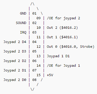
But let's see what is brought to this expansion port from Famicom?
(screenshot from wiki.nesdev.com )
Yes, another $ 4016.1 (on input), $ 4017.0-4 (on input), $ 4017.0-2 (on output), external interruption and even sound go to it I was very pleasantly surprised when I disassembled the Dandy and saw that all this is there:
True, not all models, as it turned out. But if it is, it means there is full compatibility with accessories for Famicom, and the corresponding Japanese games can use them. But let me remind you that Dandy is a very strange mixture of NES and Famicom, PAL and NTSC. The pirates produced for her both Japanese and American games, which are essentially 100% compatible, if you do not take into account these accessories and different cartridge formats.
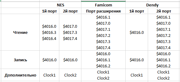
Total: in some Dandies there are all the same conclusions as on the Famikom, which at the same time include some of the conclusions available on the NES. There is no access to $ 4016.3 and $ 4016.4 , but they are rarely used. In the form of tablets for clarity:
The principle of operation of accessories
The American four-player splitter for the NES called the Four Score is a simple set of shift registers. Those. the first eight reads from $ 4016.0 give data from the first controller, and the second eight from the third. Similarly, $ 4017.0 gives data on the second and fourth controllers. In addition, when you continue reading, the device issues its signature, with which the game determines that it is the Four Score that is connected, and not something else. It turns out that such a device can be assembled from six shift registers (4021 or 74165), and it will work on any Dandy, because it does not require additional data lines. Of course, only with the American games that came out for the NES.
The Japanese counterpart for Famicom is much simpler. The third and fourth controllers are connected directly to the expansion port and are available through $ 4016.1 and $ 4017.1 . Accordingly, for such an adapter, we already need a full-fledged expansion port at the Dandy, otherwise the four of us will not be able to play Japanese games.
The Arkanoid controller, as the name implies, is used to play Arkanoid and is a twist-knob and one button. Inside it is an analog-to-digital converter and a shift register, which also consistently gives the position of the handle. The difference between the Japanese and American versions is only in the connection method. The Japanese version of the game reads the position of the knob and the state of the button from $ 4016.1 and $ 4017.1 , and the American version from $ 4016.3 and $ 4016.4, respectively. It turns out that for the Japanese Arkanoid you need a full-fledged expansion port, and for the American any dandy is suitable where the light gun works (it uses the same conclusions).
Creating your own accessory
Although the above devices themselves have a simple scheme and are assembled from the simplest logical components, for the heart of an all-in-one device I decided to use FPGAs. Moreover, I wished to make a simple switch switch there, but I wanted to make it possible to switch buttons A and B. First, I chose Altera EPM3064ATC100 , but it soon became clear that 64 macro cells were not enough for me, and the choice fell on EPM3128ATC100 , where there are already 128 macrocells.
If it comes to that, I decided not to have a trifle at all and put some kind of screen into the device, which would display the current mode and menu with settings, besides, I have had one sign for the synthesis of the “16x2” display for a long time. I already need a microcontroller to work with it, and I chose ATMEGA16 .
It has always been the hardest thing for me to give a device a nice look. Still, I am a programmer, not a designer, but it was during the manufacture of the device as a gift I wanted to make it as beautiful and convenient as possible. Moreover, this is almost the only way to somehow show others your work of art: photos and videos are not something, according to ready-made schemes and 3D models such things recreate units, mass production is difficult to set up, but a gift is the very thing.
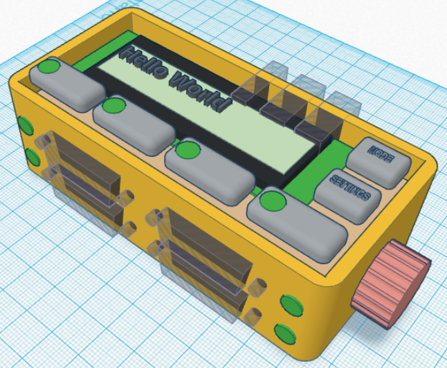
So, the appearance requirements were as follows: four ports for standard DB-15 controllers from Dandy, four buttons for selecting and configuring them, a “mode” button, a “settings” button, a convenient handle for Arkanoid and a button for it that should to settle down conveniently and not to interfere. In addition, I wanted to make the active ports illuminate with LEDs and somehow intuitively communicate with the corresponding buttons, it’s most logical to arrange the connectors in a row, but these stupid DB-15s are too huge for that. In addition to all the device should be comfortable in the hands, because it is in itself a game controller for Arkanoid. In the end, I came to something like this:
Buttons in a row, ports on top of each other, handle on the side, button for Arkanoid back left.
It turns out that there is a lot of space inside. Therefore, I decided to carry out the FPGA with connectors for wires and nests to one board, and a microcontroller with a screen and buttons to another. They are connected with the simplest serial interface.
Board with FPGA (first version):
The second board:
I wrote the code for FPGAs on Verilog. For each mode, it turns out quite simple. First of all, for many of them, we need to consider calls to each of the ports, i.e. impulses on wire clock:
reg [4:0] counter1; reg [4:0] counter2; always @ (posedge strobe_in, posedge clock1_in) begin if (strobe_in) counter1 <= 1; else if (counter1 < 31) counter1 <= counter1 + 1; end always @ (posedge strobe_in, posedge clock2_in) begin if (strobe_in) counter2 <= 1; else if (counter2 < 31) counter2 <= counter2 + 1; end (sorry, habr doesn't know how to highlight Verilog)
Where strobe_in is strobe (one on both ports), and clock1_in and clock2_in are respectively clock on each of the ports. Inside the console there is a logic: clock = R / W nand (address == $ 4016 / $ 4017), i.e. on clock is a logical zero when the console reads the data at the corresponding address.
The imitation mode of the American splitter for four players looks like this:
always @ (*) begin // Strobe - assign strobe_out[0] = strobe_in; assign strobe_out[1] = strobe_in; assign strobe_out[2] = strobe_in; assign strobe_out[3] = strobe_in; // clock , clock_out[0] <= (counter1 <= 8) ? clock1_in : 1; clock_out[1] <= (counter2 <= 8) ? clock2_in : 1; clock_out[2] <= (counter1 > 8 && counter1 <= 16) ? clock1_in : 1; clock_out[3] <= (counter2 > 8 && counter2 <= 16) ? clock2_in : 1; if (counter1 <= 8) // joy1_data_out[0] <= joy_data[0]; else if (counter1 <= 16) // joy1_data_out[0] <= joy_data[2]; // else if (counter1 == 20) joy1_data_out[0] <= 0; else joy1_data_out[0] <= 1; // if (counter2 <= 8) joy2_data_out[0] <= joy_data[1]; // else if (counter2 <= 16) joy2_data_out[0] <= joy_data[3]; // else if (counter2 == 19) joy2_data_out[0] <= 0; else joy2_data_out[0] <= 1; // , VCC joy1_data_out[1] <= 1'bZ; joy2_data_out[4:1] <= 4'bZZZZ; end In the mode of a Japanese splitter for four, you just need to connect the inputs to the outputs directly:
always @ (*) begin clock_out[0] <= clock1_in; clock_out[1] <= clock2_in; clock_out[2] <= clock1_in; clock_out[3] <= clock2_in; joy1_data_out[0] <= joy_data[0]; joy2_data_out[0] <= joy_data[1]; joy1_data_out[1] <= joy_data[2]; joy2_data_out[1] <= joy_data[3]; // , VCC joy2_data_out[4:2] <= 3'bZZZ; end The most difficult thing was to make it possible to swap buttons A and B, because they are read sequentially, that is, you need to know in advance the value of B when the console requests A, but it is issued just after A. At first, I thought to somehow speedily read data from the controller using some external clock generator, but in the end I decided to just take the value from the previous read . This gives a delay, but it is completely invisible. Moreover, games usually read the state of the buttons several times in a row.
Of course, all these modes and settings must somehow be set. To do this, I defined a 12-bit control register, which is written to it via a serial connection, with an additional parity bit:
reg [11:0] control; reg control_parity; reg [11:0] control_receiver; reg [3:0] control_counter; always @ (posedge control_strobe, posedge control_clock) begin if (control_strobe) begin control_counter = 0; control_parity = 0; end else begin if (control_counter <= 11) begin control_receiver[control_counter] = control_data; control_parity = control_parity ^ control_data; end; if (control_counter < 12) control_counter = control_counter + 1; end end always @ (posedge strobe_in) begin if (control_counter == 12 && !control_parity) control = control_receiver; end Accordingly, from the side of the microcontroller, the code (very dirty) looks like this:
void control_send(uint16_t data) { set_bit(CTRL_PORT, CTRL_STROBE_PIN); // Strobe _delay_us(10); unset_bit(CTRL_PORT, CTRL_STROBE_PIN); // Strobe _delay_us(10); int b; char parity = 0; for (b = 0; b < 11; b++) { if (data & (1<<b)) { set_bit(CTRL_PORT, CTRL_DATA_PIN); // Data parity ^= 1; } else { unset_bit(CTRL_PORT, CTRL_DATA_PIN); // Data } unset_bit(CTRL_PORT, CTRL_CLOCK_PIN); // Clock _delay_us(10); set_bit(CTRL_PORT, CTRL_CLOCK_PIN); // Clock _delay_us(10); } if (parity) { set_bit(CTRL_PORT, CTRL_DATA_PIN); // Data } else { unset_bit(CTRL_PORT, CTRL_DATA_PIN); // Data } unset_bit(CTRL_PORT, CTRL_CLOCK_PIN); // Clock _delay_us(10); set_bit(CTRL_PORT, CTRL_CLOCK_PIN); // Clock _delay_us(10); } The rest of the microcontroller code is nothing special: working with the display on the HD44780 controller, buttons, LEDs, a simple menu and working with the analog-to-digital converter to determine the angle of rotation of the handle.
I debugged everything, I was convinced of working capacity and I already started stuffing the components into the case ...
But before closing the lid I decided to check on the original Famicom, because the device will also be used with it. Alas, the modes where it was necessary to count clock pulses did not work correctly. With the help of a logic analyzer, it turned out that the data line leads to a clock line:
This is a noise of only a few tens of nanoseconds that spoils everything. I decided to see with my simple oscilloscope what happens on the Dandy clock line:
And here that in the same at Famikom:
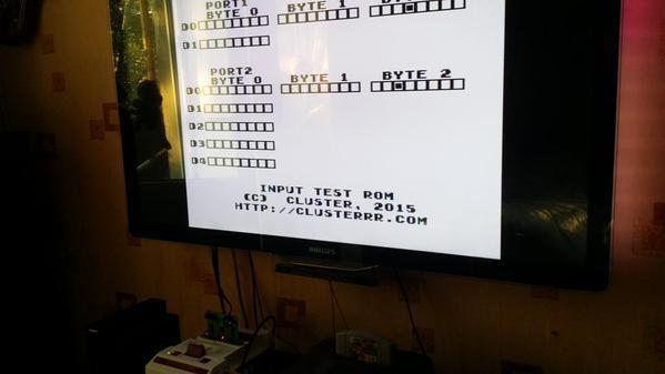
It can be seen that this line is pulled to VCC, with what is very strong in Dandy and very weak in the original Famikom. I started experimenting with the kit. It soon became clear that it was better to look at the result not with a logical analyzer, but with the console itself. I had to remember the assembler for the 6502 processor, write a simple program for testing and write it to the cartridge:
It immediately became clearly visible, and at the same time it was possible to test all modes at once, without changing the game. ROM can be downloaded here .
As a result, the problem was solved by tightening the clock lines to the VCC through a 1 kOhm resistor, a capacitor between the clock and the ground at 22nF, and 200 ohm resistors into the break of all data lines. Alas, I had to poison a new board (I did not photograph it), but after that everything immediately worked.
The final view of the device:
In Soviet times, I could be a good industrial designer.
Many probably will want to see the video, but at the moment the gift is already in the hands of our mail, and I shot only a small video instruction for the end user. You can see it here: www.youtube.com/watch?v=39beci7nE8w
And if you are interested in the themes of the work of various game controllers and the creation of self-made ones, we just shot the second series of our show “While everyone is playing” on this topic, where a lot is very simply and clearly explained to those who are not at all in the subject:
http://www.youtube.com/watch?v=nG-QznTyQKA
Information on the architecture of these consoles and accessories was taken from the site wiki.nesdev.com
Full code for FPGAs on Verilog: pastebin.com/nt39ZGvH
Source: https://habr.com/ru/post/260749/
All Articles