InGaAs Semiconductor as an Alternative to Silicon
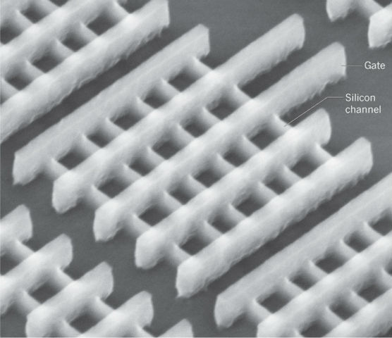
Since 1960, the structure of the transistors, created by the team of Jay Last, has not changed. Metal Oxide Semiconductor, abbreviated MOS transistors are the main part of modern computer microchips. For 55 years, the technological process of elements of computer microchips has decreased significantly, to 14 nm (Broadwell top processor).

For all these years, many improvements have been introduced in production, the structure of microcircuits began to grow not only in width / length, but also in height. Now the structure of the CPU is reminiscent of the "metropolis". But over all these years, the main component has remained unchanged - silicon, like 55 years ago, is still the main part of the chip today. Unfortunately, and perhaps fortunately, this cannot continue forever, silicon has a limit, it will not allow to reduce the process below 10 nm without loss of productivity, Intel engineers said.
Despite all this, the company voiced its plans for the future - to achieve those. process at 7 nm for its microchips by 2018. The statement is good, but you can say anything, it’s a different matter to fulfill the plans. We will be able to find out only after 3 years, although taking into account the fact that the release of Broadwell has been postponed several times, it is possible to wait more. And yet one thing pleases, they have a plan.
')

This plan is simple - instead of silicon, use a semiconductor. The successor to silicon should have greater mobility. Mobility is the coefficient of proportionality between carrier drift and external electric field. By carrier drift, we mean the purposeful average velocity of an electron moving under the influence of an external electric field. Mobility is very important in this area, as its higher value allows producing more dense, faster chips reducing their power consumption.
2016 promises us the development of 10 nm production process technology for the CPU, such as those. The process is quite feasible when using classic materials. But now 2018 promises to be much more interesting, since according to all the same Intel representatives, the production of 7 nm chips using the classic approach is no longer possible.
Fingering various elements from the periodic table of Mendeleev, has borne fruit. Various candidates have been put forward for the role of alternative materials instead of the usual silicon. The base cell of microprocessors is not a single transistor, but a minimum of a pair of complementary (complementary) MOS transistors - CMOS for short. Such transistors are n-channel and p-channel. For n-channel transistors it is planned to use InGaAs compound from indium-gallium arsenide. For p-channel transistors, the candidate was germanium from group IV, chemically bound to silicon. However, this choice is not final. The above materials have a higher mobility than silicon.
Opinion David House from Intel: "Processor performance should double every 18 months," became the slogan for Intel, which they adhere to. Achieving this result is only possible if the Moore's law is observed: "The number of transistors on an integrated circuit doubles every 24 months", - but only the evolution of transistors and their manufacturing technology made it possible to extend the law for several generations, for these reasons, companies will have to move away from silicon transistors.
In recent years, it has been difficult for Intel to adhere to this law. This is confirmed by the fact that the release of a microchip with a 14 nm technological process of Broadwell was postponed several times, as I mentioned earlier. At first glance, it is not very clear why the development and release of Broadwell was delayed, since this is essentially the second generation of microchips from Intel. The first experimental transistor with Tri-Gate technology was introduced back in 2006. The firstborn of the generation of 22 nm microchips with Tri-Gate technology was the Ivy Bridge, which was released into mass production at the end of 2011.
Obviously, one of the problems was the increase in the number of masks in the photolithography process. This is presumably associated with the problems of using 193 nm ultraviolet radiation for images with a sub-wavelength of 14 nm. Over the years of development and improvement of subwave lithography, many workarounds have been found that improved various aspects, such as: correction of optical proximity, phase transition of masks, immersion in liquids with a high refractive index, and repeated exposure, which caused an increase in the number of masks .
Although the idea and development of extreme ultraviolet lithography from a wavelength close to 13 nm originated before 2000, it was soon folded and resumed only after the appearance of 100 nm chips in the first half of the 2000s. At the moment, the success of the development of this technology is not expected until the beginning of the 7 nm era of the production process. One of the main problems is finding the source of energy for the beam. More shortwave radiation is strongly absorbed by all substances. One can only think about using mirror optics placed in a vacuum with reflection based on interlayer interference. The mask (photomask) is also performed as a reflecting element, rather than translucent. With each reflection, the mirror and mask absorb a significant part of the beam energy, about 1/3. When using 7 mirrors, about 94% of the beam power will be absorbed, which means that extreme ultraviolet lithography (EUL) requires powerful sources. But there is also a problem in the infrastructure of the work of ESL with different masks.
The company was not able to reduce the cost of producing microchips with a 14 nm process technology, but management adheres to the idea that the technology in its current form brings more benefits than attempts to simplify it. An experimental device with a 10 nm process technology promises to be 50% faster than the top Broadwell, and delays in its production are not expected to be important.
The use and introduction into mass production of InGaAs or other elements of the III - IV group causes a number of difficulties. The first problem that this technology has to face for creating InGaAs on substrates with a diameter of 30 cm. Making such substrates is of paramount importance for mass production of microchips, which in turn leads to a simple conclusion - it is impossible to completely eliminate the use of silicon.
In 2013, the nano-electronics center Imec, located in Leuven (Belgium), began experiments on the creation of technology for the production of silicon substrates adapted for 7 nm of those. manufacturing process, in which silicon wafers are subsequently replaced with InGaAs wafers. The European Research Center has also developed a similar process for replacing silicon wafers with wafers consisting of germanium. Other researchers are developing a different approach — building up InGaAs plates on a slightly smaller base of indium phosphide (InP), 10 cm in diameter, and then transferring them to 30 cm silicon substrates by direct bonding. However, this complicates the process, and the cost of the final product increases accordingly. This policy makes an unprofitable chip for a simple layman.
Also in the further production of InGaAs transistors should take into account such moments as the contacts of the source / outflow. Many experimental devices are too large for a 7 nm process technology and use some materials that are incompatible with silicon media.
Researchers from the United States and South Korea sounded a record combination of pre-threshold oscillation — 82 mV / decade, 0.5 V outflow bias, transconductivity — 1800 μS / μm, and current — 0.41 mA / μm for an InGaAs CMOS transistor. Epitaxial structures were grown on a semi-insulating compound of indium phosphide by means of molecular beam epitaxy. Epitaxy is a controlled buildup of one crystalline material on another. In the case of molecular beam epitaxy, the elements evaporate at a very high temperature (from 400 - 800 o C), and the use above vacuum at a pressure of 10 -6 - 10 -8 Pa ensures the deposition of molecules of elements on the surface with a lower temperature.

A multi-layered tip was used to control the spacing between the sides of the tracks, with a wet / dry pickle combination. The array creation consisted of two electron beam lithography processes to achieve the desired height and width of the gate edge. The final height and width of the ribs were 20 nm and 30 nm, respectively.
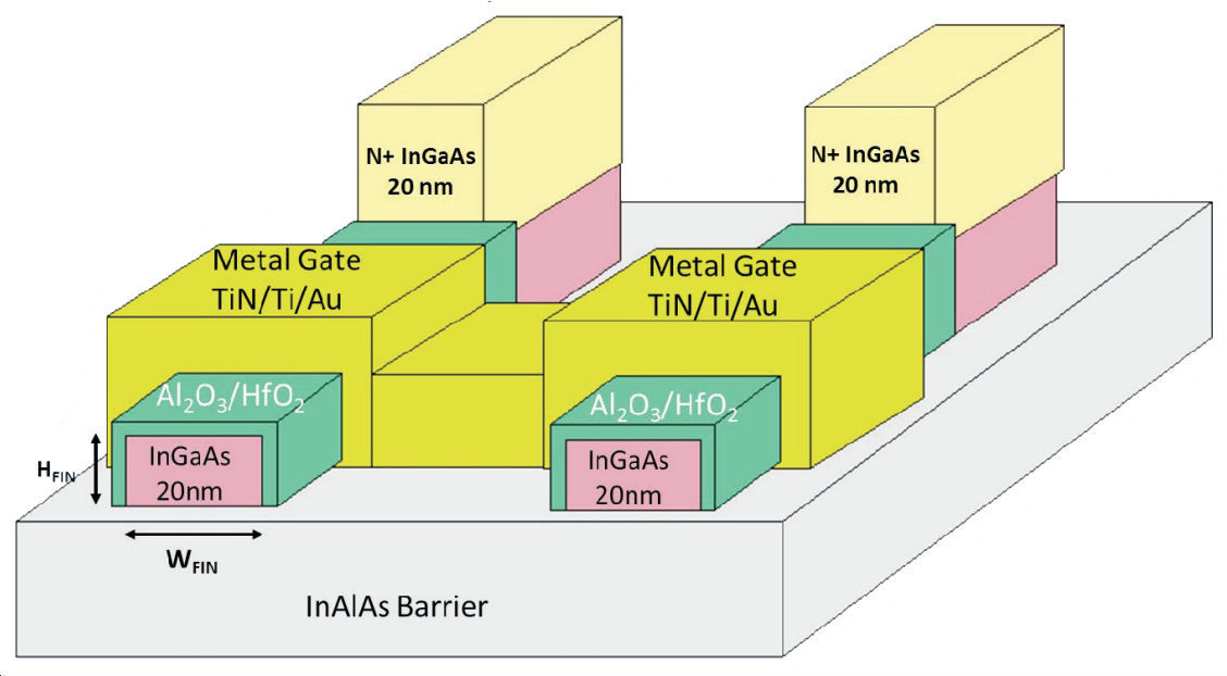
Gate 80 nm long were installed in a layer of silicon dioxide (SiO 2 ). The insulation consisted of 0.7 nm alumina (Al 2 O 3 ) and 2 nm hafnium dioxide (HfO 2 ) according to the principle of atomic layer deposition (ACO).
March 31, 2015 The Korean Institute of Science and Technology demonstrated InGaAs transistors immersed in a yttrium oxide layer. Researchers are considering InGaAs as a promising alternative to more sophisticated Tri-Gate technology. The use of Y 2 O 3 should allow to reduce the equivalent oxide thickness (EOT), compared with aluminum oxide on the basis of a higher dielectric constant (16 vs. 9-12). An interesting fact is that water has a dielectric constant of 80. Reducing the EOT allows you to place the shutter closer to the channel increasing the electrostatic control.
The MOS transistor channel was constructed by transferring an InGaAs layer grown on an indium phosphide (InP) substrate onto a silicon substrate, followed by coating with a Y 2 O 3 layer. The InGaAs surface was prepared - the natural oxide was removed and passivation was performed with a solution consisting of acetone, ammonium hydroxide and ammonium sulfide. The cleaned surface was coated with 10 nm Y 2 O 3 deposited by electron beam evaporation. The silicon substrate was also coated with 10 nm of Y 2 O 3 , after purification with hydrofluoric acid.
The waffle joint was achieved by manual air pressure. The growth substrate InP and the protective layer of InGaAs were removed using hydrochloric and phosphoric acid, by wet etching. Nickel and gold were used for the source and outflow electrodes. InP was partially corroded in the area of the source and outflow, it had to be removed completely, but it remains in the canal area to reduce the impact on the surface, which can affect mobility.
The final device was subjected to rapid thermal annealing at 300 o C. The length of the gate and the channel (body) was 2 μm with a thickness of 10 nm. The subthreshold oscillation was 90mV / decade, which was described by the researchers as “very low” due to the relatively large EOT. Effective mobility was increased 2.5 times compared to silicon-based devices, even without annealing. Annealing at 300 o C increased the effective mobility up to 2000 cm 2 (V · s). According to the researchers, these first indicators can be improved with process optimization.
All of the above are experiments, innovations, attempts to reach new heights. We will not deny that this process can be quite lengthy and fraught with many failures and failures. However, this is exactly how the very innovations that will eventually become an integral part of our life are born.
For all these years, many improvements have been introduced in production, the structure of microcircuits began to grow not only in width / length, but also in height. Now the structure of the CPU is reminiscent of the "metropolis". But over all these years, the main component has remained unchanged - silicon, like 55 years ago, is still the main part of the chip today. Unfortunately, and perhaps fortunately, this cannot continue forever, silicon has a limit, it will not allow to reduce the process below 10 nm without loss of productivity, Intel engineers said.
Despite all this, the company voiced its plans for the future - to achieve those. process at 7 nm for its microchips by 2018. The statement is good, but you can say anything, it’s a different matter to fulfill the plans. We will be able to find out only after 3 years, although taking into account the fact that the release of Broadwell has been postponed several times, it is possible to wait more. And yet one thing pleases, they have a plan.
')
This plan is simple - instead of silicon, use a semiconductor. The successor to silicon should have greater mobility. Mobility is the coefficient of proportionality between carrier drift and external electric field. By carrier drift, we mean the purposeful average velocity of an electron moving under the influence of an external electric field. Mobility is very important in this area, as its higher value allows producing more dense, faster chips reducing their power consumption.
2016 promises us the development of 10 nm production process technology for the CPU, such as those. The process is quite feasible when using classic materials. But now 2018 promises to be much more interesting, since according to all the same Intel representatives, the production of 7 nm chips using the classic approach is no longer possible.
Fingering various elements from the periodic table of Mendeleev, has borne fruit. Various candidates have been put forward for the role of alternative materials instead of the usual silicon. The base cell of microprocessors is not a single transistor, but a minimum of a pair of complementary (complementary) MOS transistors - CMOS for short. Such transistors are n-channel and p-channel. For n-channel transistors it is planned to use InGaAs compound from indium-gallium arsenide. For p-channel transistors, the candidate was germanium from group IV, chemically bound to silicon. However, this choice is not final. The above materials have a higher mobility than silicon.
Opinion David House from Intel: "Processor performance should double every 18 months," became the slogan for Intel, which they adhere to. Achieving this result is only possible if the Moore's law is observed: "The number of transistors on an integrated circuit doubles every 24 months", - but only the evolution of transistors and their manufacturing technology made it possible to extend the law for several generations, for these reasons, companies will have to move away from silicon transistors.
In recent years, it has been difficult for Intel to adhere to this law. This is confirmed by the fact that the release of a microchip with a 14 nm technological process of Broadwell was postponed several times, as I mentioned earlier. At first glance, it is not very clear why the development and release of Broadwell was delayed, since this is essentially the second generation of microchips from Intel. The first experimental transistor with Tri-Gate technology was introduced back in 2006. The firstborn of the generation of 22 nm microchips with Tri-Gate technology was the Ivy Bridge, which was released into mass production at the end of 2011.
Obviously, one of the problems was the increase in the number of masks in the photolithography process. This is presumably associated with the problems of using 193 nm ultraviolet radiation for images with a sub-wavelength of 14 nm. Over the years of development and improvement of subwave lithography, many workarounds have been found that improved various aspects, such as: correction of optical proximity, phase transition of masks, immersion in liquids with a high refractive index, and repeated exposure, which caused an increase in the number of masks .
Although the idea and development of extreme ultraviolet lithography from a wavelength close to 13 nm originated before 2000, it was soon folded and resumed only after the appearance of 100 nm chips in the first half of the 2000s. At the moment, the success of the development of this technology is not expected until the beginning of the 7 nm era of the production process. One of the main problems is finding the source of energy for the beam. More shortwave radiation is strongly absorbed by all substances. One can only think about using mirror optics placed in a vacuum with reflection based on interlayer interference. The mask (photomask) is also performed as a reflecting element, rather than translucent. With each reflection, the mirror and mask absorb a significant part of the beam energy, about 1/3. When using 7 mirrors, about 94% of the beam power will be absorbed, which means that extreme ultraviolet lithography (EUL) requires powerful sources. But there is also a problem in the infrastructure of the work of ESL with different masks.
The company was not able to reduce the cost of producing microchips with a 14 nm process technology, but management adheres to the idea that the technology in its current form brings more benefits than attempts to simplify it. An experimental device with a 10 nm process technology promises to be 50% faster than the top Broadwell, and delays in its production are not expected to be important.
The use and introduction into mass production of InGaAs or other elements of the III - IV group causes a number of difficulties. The first problem that this technology has to face for creating InGaAs on substrates with a diameter of 30 cm. Making such substrates is of paramount importance for mass production of microchips, which in turn leads to a simple conclusion - it is impossible to completely eliminate the use of silicon.
In 2013, the nano-electronics center Imec, located in Leuven (Belgium), began experiments on the creation of technology for the production of silicon substrates adapted for 7 nm of those. manufacturing process, in which silicon wafers are subsequently replaced with InGaAs wafers. The European Research Center has also developed a similar process for replacing silicon wafers with wafers consisting of germanium. Other researchers are developing a different approach — building up InGaAs plates on a slightly smaller base of indium phosphide (InP), 10 cm in diameter, and then transferring them to 30 cm silicon substrates by direct bonding. However, this complicates the process, and the cost of the final product increases accordingly. This policy makes an unprofitable chip for a simple layman.
Also in the further production of InGaAs transistors should take into account such moments as the contacts of the source / outflow. Many experimental devices are too large for a 7 nm process technology and use some materials that are incompatible with silicon media.
Increased oscillation and transconductivity
Researchers from the United States and South Korea sounded a record combination of pre-threshold oscillation — 82 mV / decade, 0.5 V outflow bias, transconductivity — 1800 μS / μm, and current — 0.41 mA / μm for an InGaAs CMOS transistor. Epitaxial structures were grown on a semi-insulating compound of indium phosphide by means of molecular beam epitaxy. Epitaxy is a controlled buildup of one crystalline material on another. In the case of molecular beam epitaxy, the elements evaporate at a very high temperature (from 400 - 800 o C), and the use above vacuum at a pressure of 10 -6 - 10 -8 Pa ensures the deposition of molecules of elements on the surface with a lower temperature.
A multi-layered tip was used to control the spacing between the sides of the tracks, with a wet / dry pickle combination. The array creation consisted of two electron beam lithography processes to achieve the desired height and width of the gate edge. The final height and width of the ribs were 20 nm and 30 nm, respectively.
Gate 80 nm long were installed in a layer of silicon dioxide (SiO 2 ). The insulation consisted of 0.7 nm alumina (Al 2 O 3 ) and 2 nm hafnium dioxide (HfO 2 ) according to the principle of atomic layer deposition (ACO).
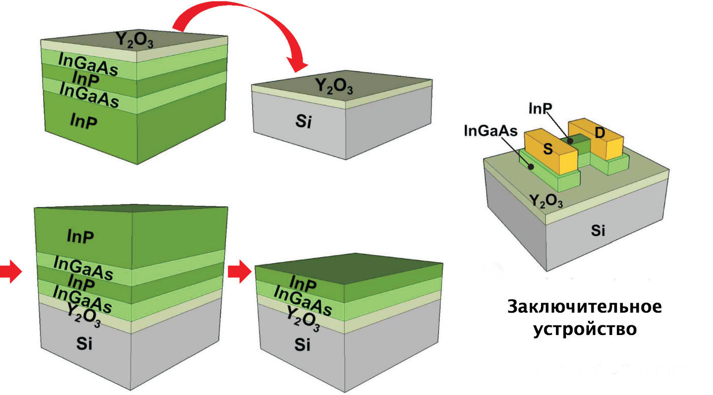
Yttrium oxide insulation
March 31, 2015 The Korean Institute of Science and Technology demonstrated InGaAs transistors immersed in a yttrium oxide layer. Researchers are considering InGaAs as a promising alternative to more sophisticated Tri-Gate technology. The use of Y 2 O 3 should allow to reduce the equivalent oxide thickness (EOT), compared with aluminum oxide on the basis of a higher dielectric constant (16 vs. 9-12). An interesting fact is that water has a dielectric constant of 80. Reducing the EOT allows you to place the shutter closer to the channel increasing the electrostatic control.
The MOS transistor channel was constructed by transferring an InGaAs layer grown on an indium phosphide (InP) substrate onto a silicon substrate, followed by coating with a Y 2 O 3 layer. The InGaAs surface was prepared - the natural oxide was removed and passivation was performed with a solution consisting of acetone, ammonium hydroxide and ammonium sulfide. The cleaned surface was coated with 10 nm Y 2 O 3 deposited by electron beam evaporation. The silicon substrate was also coated with 10 nm of Y 2 O 3 , after purification with hydrofluoric acid.
The waffle joint was achieved by manual air pressure. The growth substrate InP and the protective layer of InGaAs were removed using hydrochloric and phosphoric acid, by wet etching. Nickel and gold were used for the source and outflow electrodes. InP was partially corroded in the area of the source and outflow, it had to be removed completely, but it remains in the canal area to reduce the impact on the surface, which can affect mobility.
The final device was subjected to rapid thermal annealing at 300 o C. The length of the gate and the channel (body) was 2 μm with a thickness of 10 nm. The subthreshold oscillation was 90mV / decade, which was described by the researchers as “very low” due to the relatively large EOT. Effective mobility was increased 2.5 times compared to silicon-based devices, even without annealing. Annealing at 300 o C increased the effective mobility up to 2000 cm 2 (V · s). According to the researchers, these first indicators can be improved with process optimization.
All of the above are experiments, innovations, attempts to reach new heights. We will not deny that this process can be quite lengthy and fraught with many failures and failures. However, this is exactly how the very innovations that will eventually become an integral part of our life are born.
Source: https://habr.com/ru/post/259027/
All Articles