Pulse sensor device Part 2 - Sensors
In this article you will learn about several details that need to be paid attention to when designing photoplethysmograph sensors.
Introduction
In the previous article you got acquainted with the design of the sensor measuring the pulsogram . Today I will share some ideas that may be useful in choosing the element base of the plethysmograph and developing its electrical circuit. They will help to improve the quality of the useful signal, which is primarily influenced by the following factors:
- lack of artifacts;
- the presence of a pronounced pulse wave at the point of registration;
- sensitive element design.
An artifact is a non-useful component of a change in the waveform, spectrally and amplitudely similar to it.
')
There are several sources of artifacts:
- the movement of the person using the photoplethysmograph, the relative source of illumination, natural or artificial, for example, the movement of the sun shade during sports activities;
- moving the light source relative to a person or changing the brightness of that source. For example, flickering fluorescent lamps;
- non-pulse movements of body parts causing movements of the photoplethysmograph or points of the body in the place where the sensitive element is installed. For example, movements of the bones of the forearm that occur when moving with your fingers, movements of the bones of the head associated with speech and facial expressions.
In addition to artifacts, the quality of pulse measurement depends on the severity of the pulse wave. For the same person, the pulse can be very good and very bad. For example, I have watched a change in the pulse many times during a three-hour computer psycho-physiological testing. Pulsogram was measured from the earlobe. At the same time, the signal deteriorated over time. This could happen quite quickly - in half an hour, and is connected, presumably, with the fact that the ear clip degrades the blood flow, as well as with the forced immobility of the subject.
A similar situation is observed when measuring the pulse from the phalanx of the finger. A change in temperature in a room or a slight change in a person’s posture and the resulting shift of the registration point by a small distance can lead to a decrease in the signal level or even to its disappearance.
When measuring the pulse from the temple, the problem of lack of signals is exacerbated. The area of the temple is larger than the area of the finger, it is more difficult to find the point at which the pulse is better manifested, and there is a greater chance that the user will put the sensor on incorrectly.
Multichannel Sensors
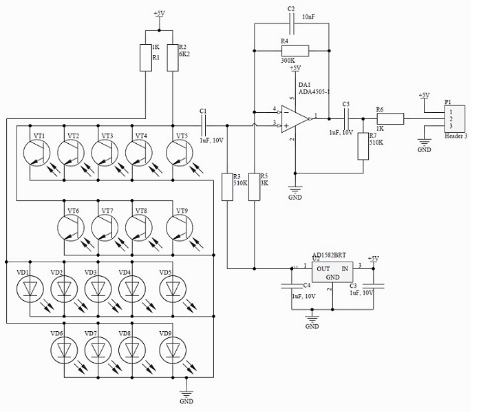
To solve the described problem, the principle common in engineering can be applied - duplication, which in this case implies the use of a sensor with several sensitive elements. A schematic diagram that implements such an idea is shown in the following figure.
I foresee skeptical thoughts of readers about parallel-on LEDs. I ask you not to judge strictly, since this is a prototype, which should not have been operated for a long time.
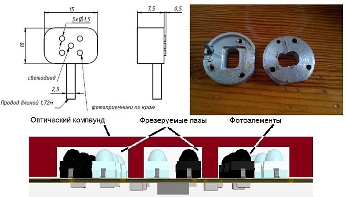
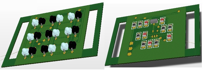
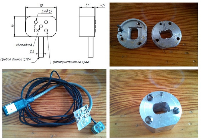
The LEDs and phototransistors on the PCB are arranged in pairs. The size of the board is chosen so as to overlap the entire area of the temple, this allows you to have a gain and filtering circuit in the same place. The board may contain holes for attachment to the tape. The appearance of the sensor with nine sensitive elements is presented in the following figure.
A similar solution can be applied to measure the pulse from a finger or wrist. Below is a diagram of a sensor consisting of four phototransistors and one LED.
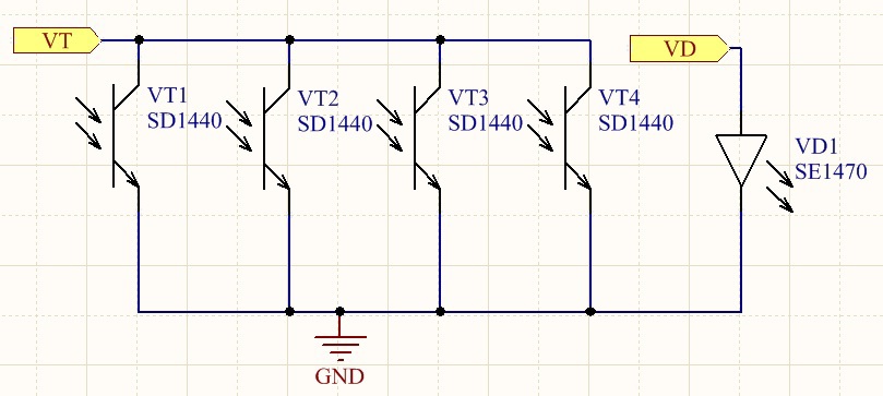
Phototransistor emitters may not be connected, and then the signals from each of them are measured independently, in which case a special multi-channel measuring device is required. Multi-channel execution can also be useful for eliminating artifacts. If an artifact occurs only in the region of a single photocell, it is fixed and not taken into account in the overall measurement pattern. However, the use of such a scheme is not always convenient, since it leads to an increase in size. It is quite another thing if you connect the photosensitive elements in parallel. In this case, only one measuring channel is required. The following figure shows a prototype of such a sensor. It works according to the “reflection” scheme. The LED is located in the center, and the phototransistors are on the edges. The sensor can be used to record a pulsogram with a phalanx of a finger or wrist. The printed circuit board is divorced so as to be able to connect phototransistors to multichannel or single-channel versions.
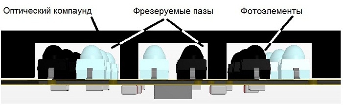
Compounding
For better fixation of photocells, the surface of the printed circuit board can be filled with compound. For the fill is made a special form, which you also see in the picture. To the compound does not stick to the form, it is better to make it from fluoroplastic. If the form is made of a different material, for example, of metal, then before pouring the compound, it should be smeared with a special compound. If such a composition is not available, suitable petroleum jelly. You should also carefully choose the compound, as the wrong composition can deform the elements during curing.
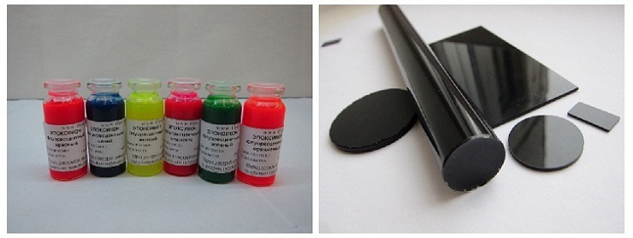
In addition to fixing the compound performs the role of a light filter. Epoxy compounds with dyes are suitable for this purpose. For example, the compound “Epoxicon” manufactured by SPbGTI can be used.
An alternative to compounds can make solid filters. They closely adjoin to the printed circuit board, and for LEDs and phototransistors grooves are made with a cutter or laser. The following figure shows a sensor with elements covered with a milled plate.
Existence of the light filter allows to minimize the artifacts created by external light sources. The following image shows the appearance of the optical compounds before and after curing.
Photos from this site
Features of the choice of phototransistors and LEDs
To register a pulse wave, photosensitive elements are used - photodiodes or phototransistors. This article deals only with phototransistors. Because at the time of my beginning of work in this direction, there were already dozens of different transistor sensors (clips, clothespins and napalechnikov) on their hands, and there were also well-established circuit solutions. The use of diodes is no worse at all and is widely used in various applications, for example, in common medical sensors of the Nellcor standard.
When choosing phototransistors and LEDs, first of all you should pay attention to the following characteristics:
- wavelength (maximum spectral characteristics) [nm];
- half brightness angle for LEDs and coverage angle for phototransistors [deg.];
- radiation intensity [mW / sr] for LEDs and sensitivity for phototransistors [mA / (mW / cm2)];
- rated current of phototransistor and LED [mA];
- phototransistor dark current [mA];
- presence of lenses and light filters built into the body.
To measure the pulse is best suited wavelengths that are most absorbed by the blood. These are waves corresponding to the green color of 530 nm. Red and infrared bands are also used. I highly recommend an interesting article on giktime with the classification of methods for measuring the pulse, in the same place you will learn about the absorption spectrum of hemoglobin.
When choosing photocells, you should pay attention to the presence of lenses and light filters that allow you to achieve the desired angle of half brightness and coverage, and, therefore, be less sensitive to radiation from other sources. Built-in filters allow you to work only in the selected spectral range. If you choose a LED with a large angle of half brightness and a phototransistor with a large angle of coverage, then the light will pass, bypassing the skin surface. This will lead to a deterioration of the measuring range and the luminous flux modulated by the pulse wave will have almost no effect on the output signal of the measuring circuit. This situation is illustrated in the following figure.
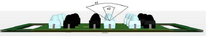
Angle a2 is valid, and angle a1 is too big to use an LED with that angle in the pulse measurement device. This example refers to the case of the measurement of the pulse "on reflection". The choice of an LED with a high angle of half brightness in devices that work "in the light" will lead to the fact that a large radiation power will pass by the photodetector. This is undesirable, especially in mobile devices.
Attention should also be paid to the radiation intensity of the LED, measured in milliwatts per steradian [mW / sr]. In documents for LEDs, it is usually indicated at currents of 20, 100 and 1000 mA. To save energy, it is better to choose the LEDs, in which this characteristic is higher with the same consumed current. Attention should be paid to the photoelectric current of the phototransistor; the larger its value, the better. The last two characteristics are related. As a result, the minimum expected signal level should be at least several times higher than the expected noise level in the measuring device.
LEDs and phototransistors are often sold in pairs that are structurally and spectrally suitable for each other. The table shows the characteristics of several pairs of LEDs and phototransistors. Pairs in lines 2 and 3 are not suitable for use in heart rate monitors due to the large angle and low radiation power. Couples 1, 4 and 5 are suitable, with the first pair best suited. This was confirmed by testing. All other things being equal, the best signal of the pulsogram was taken using the first pair. It should be noted that if an opaque barrier is placed between the LED and the phototransistor, then the radiation angle and sensitivity will not so much influence the quality of the pulse measurement.
| Mark transistor -diode | Angle of coverage and angle of half brightness [hail] | Wavelength [nm] | Radiation intensity [mW / Wed] at current 20mA (for LEDs) | Photoelectric current [mA] at 1 mW per cm2 (for phototransistor) |
| VEMT2020X01 VSMB2020X01 | ± 15 ± 12 | 830-950 940 | eight | 6 |
| PT100MF0MP1 GL100MD1MP1 | ± 15 ± 80 | 910 940 | 0.3 | 2 |
| TEMT7000X01 VSMB1940X01 | ± 60 ± 60 | 830-950 940 | 1.2 | 0.45 |
| OP571 OP271 | ± 25 ± 25 | 910 890 | 1.5 | 0.5 |
| SD1440 SE1470 | ± 12 ± 12 | 880 880 | - | 0.14 |
Conclusion Three in one
Instead of the conclusion I will mention the remarkable integral decision which in the comments to the previous article was brought by the habrew user valexey . We are talking about the device Si1143 production Silicon Labs. Inside it has two photodiodes - red and IR, a control unit for three LEDs, a built-in gain and filtering circuit, an ADC and an I2C serial interface module. I will not describe other details, because I have not had time to try it out yet. Judging by the description, this device is well suited for various measurements related to pulsometry.
PS
The repository replenished with drawings of sensitive elements and intermediate amplifiers.
Source: https://habr.com/ru/post/258615/
All Articles