Reverse Engineering TL431, an extremely common chip, which you have not heard
Ken, as planned, conducted the reverse-engineering of the chip from photographs taken by BarsMonster . Bars in the article mentioned his communication with Ken, but this translated article was not yet there.
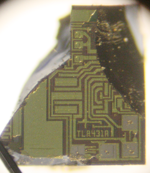
A photo of an interesting, but little-known, TL431 chip used in power supplies provides an opportunity to understand how analog circuits are implemented in silicon. Despite the fact that the diagram in the photo looks like some kind of labyrinth, the microcircuit itself is relatively simple and can be investigated without much difficulty. In my article I will try to explain how transistors, resistors and other radio components are packed in silicon to perform their functions.
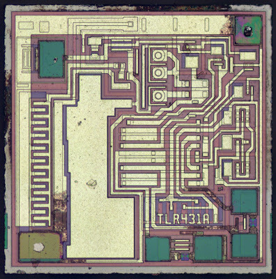
Photo of TL431 crystal. Original Zeptobars .
TL431 is a “programmable precision reference voltage source” [1] and is usually used in switching power supplies for feedback when the output voltage is too high or, conversely, is low. Using a section of a circuit called a bandgap (a source of reference voltage, the magnitude of which is determined by the width of the forbidden zone), the TL431 provides a stable source of reference voltage over a wide temperature range. The TL431 block diagram shows a 2.5-volt reference source and comparator, but looking at the photo of the chip, you can see that the internal structure of the chip is different from the drawing.
')

A block diagram of the TL431 taken from the datasheet .
TL431 has a long history: it was released back in 1978 [2] , and has since been in a variety of devices. He helped stabilize the voltage in the power supply for the Apple II, and is now used in most ATX power supplies [3] and even in iPhone chargers and other devices. And MagSafe-connectors, and adapters for laptops , and microcomputers , LED drivers , power supplies for audio equipment , video consoles , TVs [4] . TL431 is present in all this electronics.
The photos below show the TL431 inside six different power supplies. TL431 is available in a variety of shapes and sizes. The two most popular form factors are shown below. [5] Perhaps the reason that the TL431 does not attract much attention is because it looks more like a normal transistor than a microchip.
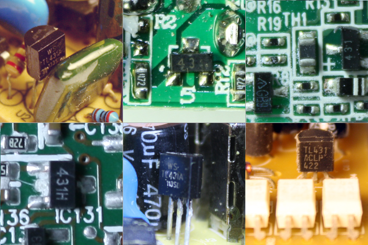
Six examples of power supply circuits using TL431. Top row: cheap 5-volt power supply unit, cheap phone storage, Apple iPhone storage (in the photo you can also notice the GB9 variation). Bottom row: MagSafe adapter, KMS USB , Dell ATX power supply unit (optocouplers in the foreground)
TL431 is a very simple microcircuit, and it is quite possible to understand its logic at the silicon level by closely studying the photo. I will show how transistors, resistors, jumpers and capacitors are implemented. And then I will conduct a full reverse-engineering of this chip.
The microcircuit uses both npn and pnp bipolar transistors (as opposed to microcircuits like 6502 , which used MOSFET). If you studied electronics at school or at a university, you may have seen the npn transistor circuit (like the one below), which shows a collector (denoted as C), a base (B) and an emitter (E). The transistor is depicted as a kind of sandwich with a P-layer between two N-layers, this arrangement of layers characterizes the transistor as npn. However, it turns out that the microcircuit has absolutely nothing similar to this circuit. Even the base is not in the center!

Symbol designation and structure of the npn transistor.
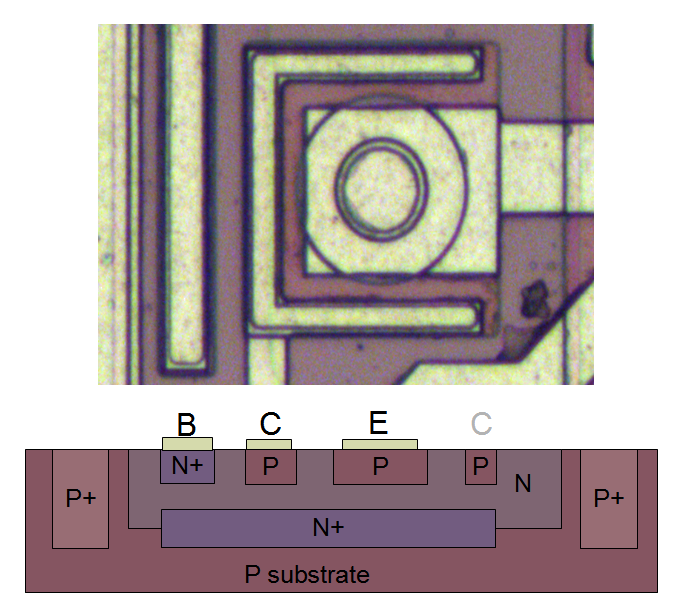
In the photo below you can see one of the transistors TL431. The color differences in the pink and purple regions are caused by different doping of silicon to form N and P regions. Light yellow areas - the metal layer of the chip, located on top of the silicon. Such areas are needed to enable the conductors to be connected to the collector, emitter and base.
At the bottom of the photo, a cross section is drawn, roughly depicting how a transistor is constructed. [6] It can be noted that there are much more details on it than in the npn sandwich from the books. However, if you look closely, you can find the very npn that forms the transistor in the cross section under the emitter (E). The emitter conductor is connected to N + silicon. Below it is a P-layer connected to the base contact. Even lower is the N + layer connected to the collector (not directly). [7] The transistor is enclosed in a P + ring for isolation from adjacent components. Since most of the transistors in TL431 belong to the npn type, then, after you have sorted out the first time, they are very easy to find in the photo and determine the necessary contacts.

The npn transistor is from a photograph of a TL431 crystal, and its structure is in silicon.
The output npn transistor is much more than the rest, since it needs to withstand the full current load. Most transistors work with microamps, and this output transistor supports a current of up to 100 milliamps. To work with such currents, it is made larger (occupies 6% of the entire crystal), and has wide metal connectors on the emitter and collector.
The topology of the output transistor is very different from other npn transistors. It is created, so to speak, sideways, a planar structure instead of a deep one, and the base is located between the emitter and the collector. The metal on the left is connected to ten emitters (bluish N-type silicon), each of which is surrounded by a pink P-layer, which is the base (middle conductor). The collector (right side) has only one big contact. The emitter and base conductors form a nested “comb”. Note that the collector metal becomes wider from top to bottom in order to maintain large currents on the bottom of the transistor.

Pnp type transistors have a completely different structure. They consist of a circular emitter (P) surrounded by a base ring (N), which, in turn, surrounds the collector (P). Thus, a horizontal sandwich is obtained, instead of the usual vertical structure of npn transistors. [eight]
The diagram below shows one of these pnp transistors, and the cross section shows a silicon structure. It is worth noting that although the metal contact for the base is in the corner of the transistor, it is electrically connected through the N and N + regions to the active ring, which lies between the collector and the emitter.
Pnp transistor structure
Resistors are a key component in almost any analog circuit. They are implemented as a long strip of doped silicon. (It seems that P-type silicon was used in this chip). Different resistances are achieved using different material areas - resistance is proportional to the area.
Three resistors are noticeable from below - they are formed by three long horizontal strips of silicon. Yellowish metallic conductors pass through them. The joints of the metal layer and the resistor look like squares. The location of these contacts and sets the length of the resistor and, accordingly, its resistance. For example, the resistance of the lower resistor is a little more than the rest because the contacts are located at a greater distance. The top two resistors are paired with a metal layer from the top left.

Resistors.
Resistors in microcircuits have very poor tolerance - resistance can vary by 20% between microcircuits due to variations in the production process. Obviously, this is a serious problem for such accurate chips as the TL431. Therefore, the TL431 is designed in such a way that the important characteristic is not the specific resistance, but the ratio of the resistances. Specific resistance values are not very important if the resistances change in the same proportion. The second method of reducing the dependence on the effect of variability is the chip topology itself. Resistors are located on parallel tracks of the same width to reduce the effect of any asymmetry in silicon resistance. In addition, they are placed next to each other to minimize deviations in the properties of silicon between different parts of the chip. In addition to all of this, in the next chapter I will discuss how to resist the chip before enclosing the chip to regulate the performance of the chip.
This is what I did not expect in the TL431, so these are jumpers for adjusting the resistances. During the production of microcircuits, these jumpers can be removed in order to adjust the resistance and improve the accuracy of the microcircuit. On some more expensive chips, there are resistances that can be removed by a laser, just burning out a part of the resistor before enclosing it. The accuracy of this method is much higher than that of jumpers.
The chain with a jumper is shown in the photo below. It contains two parallel resistors (in the photo they look like one element) and a jumper. In the normal state, this jumper shunts the resistors. In the manufacture of the chip, its characteristics can be measured, and if more resistance is required, then two probes are connected to the pads and high current is applied. This process burns the jumper, adding some resistance to the circuit. Thus, the resistance of the entire circuit can be slightly adjusted to improve the characteristics of the chip.

Jumper for setting resistance
TL431 contains only two internal capacitors, but they are made in two completely different manners.
The first capacitor (under the text “TLR431A”) is formed by a reverse biased diode (reddish and purple stripes). The inverse layer in the diode has a capacitance, which can be used to form a capacitor ( more ). The main limitation of this type of capacitor is that the capacitance resistance varies depending on the voltage, because the width of the inverse layer varies.

Capacitor formed by pn junction. Vendor line is written using metal deposited on top of silicon.
The second capacitor is designed by a completely different method, and is more like an ordinary two-plate capacitor. Not even a glance - it consists of a large metal plate with an N + silicon substrate as the second plate. In order to fit next to other parts of the chain, it has an irregular shape. This capacitor occupies about 14% of the crystal area, illustrating that the capacitors in the microcircuits use space very inefficiently. The datasheet mentions that both capacitors are 20 picoFarads, but I do not know how much you can believe this.

Capacitor.
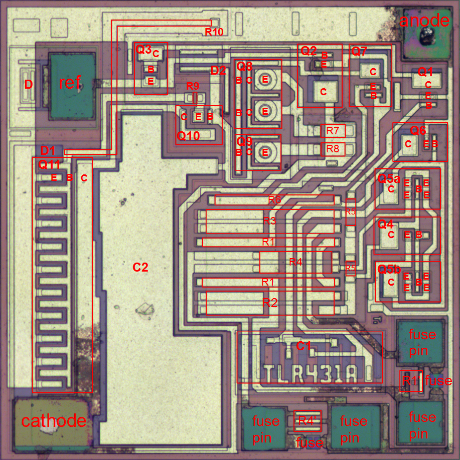
Labeled TL431 crystal.
In the diagram above, the elements on the chip are selected and named, and then transferred to the drawing below. After all the clarifications earlier, I think the structure of any element should be clear. Three pins of the microcircuit are connected to the “ref”, “anode” and “cathode” pads. The chip has one metallization level (light yellow) for connecting the components. In the drawing, the resistance is given relative to the unknown R. Probably 100 ohm is quite suitable, but I do not know the exact value. The biggest surprise was that the characteristics of the elements were very different from those that were published earlier in other schemes. These characteristics fundamentally affect how the Zener diode as a whole works with a forbidden zone voltage. [9]

TL431 drawing
TL431 operation from the outside looks pretty simple - if the contact “ref” is supplied with voltage above 2.5 volts, the output transistor conducts current between the cathode and the anode. In the power supply, this increases the current going to the control chip (indirectly), and entails a decrease in the power of the power supply, after which the voltage drops to a normal level. Thus, power supply units use TL431 in order to stably hold the required output voltage.
The most interesting part of the microcircuit is the source of the reference voltage equal to the width of the forbidden zone. [10] . The key elements are visible on the photo of the crystal: the emitter region of the transistor Q5 is 8 times larger than that of the Q4, so the two transistors react differently to temperature. The output signals from the transistors are combined through resistors R2, R3, R4 in the right proportion to compensate for temperature effects, and form a stable reference signal. [11] [12]
Voltages from a temperature-stabilized bandgap are sent to a comparator, whose input is Q6 and Q1, and Q8 and Q9 control it. Finally, the output of the comparator passes through Q10 to control the output transistor Q11.
Obtaining a photograph of a microchip crystal usually requires its dissolution in dangerous acids, and photographing the crystal itself with an expensive metallographic microscope. (Zeptobars described this process here ). I wondered what would happen if I simply broke the TL431 with clamping tongs and looked at it with a cheap microscope. In the process, I broke the crystal in half, but I still got interesting results. The image shows a large copper anode inside the case, which also works as a radiator. Next to it is a crystal (at least most of it), which was mounted on the anode inside the white circle. Noticed how much the crystal itself is smaller than its body?

TL431 body, inner anode and most of the crystal.
Using a simple microscope , I got a photo below. Despite the fact that, obviously, I did not get the same high-quality snapshot of Zeptobars, the structure of the chip is visible much better than I expected. This experiment shows that you can carry out the removal of the case of microcircuits and photographing the crystal without even touching various dangerous acids. Comparing my snapshot of cheap TL431 ordered on eBay with TL431, photographed by Zeptobars, I see their identity. Since its microcircuit does not coincide with the published drawings, I am wondering if they did not stop the production of that strange version of the microcircuit at some point. But I think that this assumption is wrong.
A piece of crystal photographed through a microscope.
Is the TL431 really the most common chip that people haven't heard about? There is no reliable way to check, but I think this is a good candidate. It seems that no one has published data in which another chip would have been produced in large quantities. Some sources claim that the 555 timer is the most common microcircuit with billions of copies every year (I don’t really believe in such a large number). But TL431 is definitely high enough in the list of prevalence. You most likely have a TL431 in some kind of device at arm's length right now (a phone charger, a laptop power adapter, a PC or monitor power supply). The difference between 555 or 741 and TL431 is that these microcircuits are so widely known that they have already become almost a part of pop culture - books , T-shirts and even circles . But if you don’t work with power supplies, the chances are quite high that you never heard of the TL431. Thus, I give my vote TL431 in such a strange nomination. If you have any other options for microcircuits that have been undeservedly bypassed, leave comments.
Crystal snapshots made by Zeptobars (except mine). Drawing and analysis are based on the work of Cristophe Basso [12] In addition, I have greatly improved my analysis through discussions with Michael from Zeptobars and the Visual 6502 group , in particular B. Engl.
1. Due to the fact that TL431 is not the most common function, a standard name for an element of this kind does not exist. Different datasheets give the following names: “adjustable shunt stabilizer” , “programmable precision reference voltage source” , “programmable shunt reference voltage source” , “programmable zener diode” . ↑
2. I unearthed the origins of the TL431 in the Voltage Regulator Handbook published by Texas Instruments in 1977. The predecessor of this chip was the TL430, released as an adjustable shunt stabilizer in 1976. The TL431 was created in the same 1976 as an update for the TL430 with improved accuracy and stability, and therefore was named as an adjustable precision shunt stabilizer. In 1977, it was announced as one of the future products of TI, and released for sale as early as 1978. Another announcement was the TL432, which would have been called the “Building block from timer / stabilizer / comparator” and consist of a reference voltage source, comparator and transistor amplifier according to a preliminary datasheet . But at the time of the release of the TL432, the plan for providing “building blocks” was forgotten. The TL432 has become an analogue of the TL431 with different contact arrangements for more convenient wiring ( datasheet ). ↑
3. Modern ATX power supplies ( example times , example two ) often contain three TL431s each. One for feedback in backup power, the second for feedback in the main power supply, and the third is taken as a linear regulator for 3.3V output voltage. ↑
4. It is interesting to look at impulse power supplies that do not use TL431. Earlier models used the reference zener diode as a reference voltage source. For example, this was practiced in the first copies of the power supply for the Apple II (Astec AA11040), but soon they replaced the Zener diode with the TL431 - Astec AA11040, revision B. In the Commodore CBM-II, model B, an unusual solution was applied - TL430 instead of TL431. The original power supply for the IBM PC used a reference zener diode (along with a bunch of operational amplifiers). Later, the PSU for the PC often used a TL494 PWM controller, which already contained a voltage source for the secondary circuit. Other BPs could contain an SG6105 , which already includes two TL431s.
Chargers for phones usually use TL431. You can rarely find a cheap fake of this element: it is easier to take the reference zener diode instead of it and save a couple of cents. Another exception may be such chargers as for the iPad . They implemented stabilization in the primary circuit and does not require any feedback at all from the output voltage. In my article about power supplies, I described this in more detail. ↑
5. The TL431 is available in more housing options than I thought. The two photographs of the TL431 are made in a “transistor” case with three legs (TO-92). The rest of the photos show the SMD version in SOT23-3. The TL431 can also be in a 4-pin, 5-pin, 6-pin and 8-pin SMD package (SOT-89, SOT23-5, SOT323-6, SO-8 or MSOP-8). In addition, it can be found in a larger version of the TO-252 or even as an 8-pin chip (DIP-8). ( pictures ). ↑
6. More detailed information about how a bipolar transistor works in silicon can be found in many places. Semiconductor Technology gives a good overview about the device npn transistor. The presentation of the Basic Integrated Circuit Processing describes in detail the production of microchips. Even the schemes with Wikipedia are very interesting. ↑
7. Perhaps you are wondering why this terminology is divided into a collector and an emitter, if they are absolutely symmetrical in our simple transistor circuit? After all, both are connected to the N-layer, what is there to differ? But as you can see in the photo of the crystal, the collector and the emitter are not only very different in size, but the doping is different. If you change the collector and emitter in some places, the transistor will have a very weak transmission coefficient . ↑
8. pnp transistors in TL431 have a circular structure, which greatly distinguishes them from npn. This circular structure is illustrated in the Designing Analog Chips book by Hans Camenzind, the author of Timer 555. If you want to know more about how analog chips work, then I recommend this book, which details this with a minimum of mathematics. Free pdf or paper version .
In addition, the structure of pnp transistors can be read in the "Principles of Semiconductor" . And the book "Analysis and Design of Analog Integrated Circuits" tells about the detailed models of bipolar transistors and how they are implemented in the microcircuits. ↑
9. , , , . . , R2 R3 1 3, Q5 Q4. , R2 R3 , Q5 8 Q4. , ΔVbe. , R1 R4 . , : Vref = 2*Vbe + (2*R1+R2)/R4 * ΔVbe 2.5 . , , . , . Q8 . , . , Q8 Q9 , . , , 2.5. B. Engl , . ↑
10. , - , , , . , , «How to make a bandgap voltage reference in one easy lesson» Paul Brokaw, . . ↑
11. , TL431 , , , . TL431 , . , -, TL431 «ref» . , «ref» , 2.5 . ↑
12. TL431, - , , . «The TL431 in Switch-Mode Power Supplies loops» — Christophe Basso Petr Kadanka. TL431 . . powerelectronics.com . «Designing with the TL431» Ray Ridley, Switching Power Magazine, , TL431 . «The TL431 in the Control of Switching Power Supplies» ON Semiconductor. , . , , , . ↑
A photo of an interesting, but little-known, TL431 chip used in power supplies provides an opportunity to understand how analog circuits are implemented in silicon. Despite the fact that the diagram in the photo looks like some kind of labyrinth, the microcircuit itself is relatively simple and can be investigated without much difficulty. In my article I will try to explain how transistors, resistors and other radio components are packed in silicon to perform their functions.
Photo of TL431 crystal. Original Zeptobars .
TL431 is a “programmable precision reference voltage source” [1] and is usually used in switching power supplies for feedback when the output voltage is too high or, conversely, is low. Using a section of a circuit called a bandgap (a source of reference voltage, the magnitude of which is determined by the width of the forbidden zone), the TL431 provides a stable source of reference voltage over a wide temperature range. The TL431 block diagram shows a 2.5-volt reference source and comparator, but looking at the photo of the chip, you can see that the internal structure of the chip is different from the drawing.
')
A block diagram of the TL431 taken from the datasheet .
TL431 has a long history: it was released back in 1978 [2] , and has since been in a variety of devices. He helped stabilize the voltage in the power supply for the Apple II, and is now used in most ATX power supplies [3] and even in iPhone chargers and other devices. And MagSafe-connectors, and adapters for laptops , and microcomputers , LED drivers , power supplies for audio equipment , video consoles , TVs [4] . TL431 is present in all this electronics.
The photos below show the TL431 inside six different power supplies. TL431 is available in a variety of shapes and sizes. The two most popular form factors are shown below. [5] Perhaps the reason that the TL431 does not attract much attention is because it looks more like a normal transistor than a microchip.
Six examples of power supply circuits using TL431. Top row: cheap 5-volt power supply unit, cheap phone storage, Apple iPhone storage (in the photo you can also notice the GB9 variation). Bottom row: MagSafe adapter, KMS USB , Dell ATX power supply unit (optocouplers in the foreground)
How do radioelectronic components look like in silicon?
TL431 is a very simple microcircuit, and it is quite possible to understand its logic at the silicon level by closely studying the photo. I will show how transistors, resistors, jumpers and capacitors are implemented. And then I will conduct a full reverse-engineering of this chip.
The implementation of transistors of various types
The microcircuit uses both npn and pnp bipolar transistors (as opposed to microcircuits like 6502 , which used MOSFET). If you studied electronics at school or at a university, you may have seen the npn transistor circuit (like the one below), which shows a collector (denoted as C), a base (B) and an emitter (E). The transistor is depicted as a kind of sandwich with a P-layer between two N-layers, this arrangement of layers characterizes the transistor as npn. However, it turns out that the microcircuit has absolutely nothing similar to this circuit. Even the base is not in the center!
Symbol designation and structure of the npn transistor.
In the photo below you can see one of the transistors TL431. The color differences in the pink and purple regions are caused by different doping of silicon to form N and P regions. Light yellow areas - the metal layer of the chip, located on top of the silicon. Such areas are needed to enable the conductors to be connected to the collector, emitter and base.
At the bottom of the photo, a cross section is drawn, roughly depicting how a transistor is constructed. [6] It can be noted that there are much more details on it than in the npn sandwich from the books. However, if you look closely, you can find the very npn that forms the transistor in the cross section under the emitter (E). The emitter conductor is connected to N + silicon. Below it is a P-layer connected to the base contact. Even lower is the N + layer connected to the collector (not directly). [7] The transistor is enclosed in a P + ring for isolation from adjacent components. Since most of the transistors in TL431 belong to the npn type, then, after you have sorted out the first time, they are very easy to find in the photo and determine the necessary contacts.
The npn transistor is from a photograph of a TL431 crystal, and its structure is in silicon.
The output npn transistor is much more than the rest, since it needs to withstand the full current load. Most transistors work with microamps, and this output transistor supports a current of up to 100 milliamps. To work with such currents, it is made larger (occupies 6% of the entire crystal), and has wide metal connectors on the emitter and collector.
The topology of the output transistor is very different from other npn transistors. It is created, so to speak, sideways, a planar structure instead of a deep one, and the base is located between the emitter and the collector. The metal on the left is connected to ten emitters (bluish N-type silicon), each of which is surrounded by a pink P-layer, which is the base (middle conductor). The collector (right side) has only one big contact. The emitter and base conductors form a nested “comb”. Note that the collector metal becomes wider from top to bottom in order to maintain large currents on the bottom of the transistor.
Pnp type transistors have a completely different structure. They consist of a circular emitter (P) surrounded by a base ring (N), which, in turn, surrounds the collector (P). Thus, a horizontal sandwich is obtained, instead of the usual vertical structure of npn transistors. [eight]
The diagram below shows one of these pnp transistors, and the cross section shows a silicon structure. It is worth noting that although the metal contact for the base is in the corner of the transistor, it is electrically connected through the N and N + regions to the active ring, which lies between the collector and the emitter.
Pnp transistor structure
The implementation of resistors in the chip
Resistors are a key component in almost any analog circuit. They are implemented as a long strip of doped silicon. (It seems that P-type silicon was used in this chip). Different resistances are achieved using different material areas - resistance is proportional to the area.
Three resistors are noticeable from below - they are formed by three long horizontal strips of silicon. Yellowish metallic conductors pass through them. The joints of the metal layer and the resistor look like squares. The location of these contacts and sets the length of the resistor and, accordingly, its resistance. For example, the resistance of the lower resistor is a little more than the rest because the contacts are located at a greater distance. The top two resistors are paired with a metal layer from the top left.
Resistors.
Resistors in microcircuits have very poor tolerance - resistance can vary by 20% between microcircuits due to variations in the production process. Obviously, this is a serious problem for such accurate chips as the TL431. Therefore, the TL431 is designed in such a way that the important characteristic is not the specific resistance, but the ratio of the resistances. Specific resistance values are not very important if the resistances change in the same proportion. The second method of reducing the dependence on the effect of variability is the chip topology itself. Resistors are located on parallel tracks of the same width to reduce the effect of any asymmetry in silicon resistance. In addition, they are placed next to each other to minimize deviations in the properties of silicon between different parts of the chip. In addition to all of this, in the next chapter I will discuss how to resist the chip before enclosing the chip to regulate the performance of the chip.
Silicon jumpers to adjust the resistance
This is what I did not expect in the TL431, so these are jumpers for adjusting the resistances. During the production of microcircuits, these jumpers can be removed in order to adjust the resistance and improve the accuracy of the microcircuit. On some more expensive chips, there are resistances that can be removed by a laser, just burning out a part of the resistor before enclosing it. The accuracy of this method is much higher than that of jumpers.
The chain with a jumper is shown in the photo below. It contains two parallel resistors (in the photo they look like one element) and a jumper. In the normal state, this jumper shunts the resistors. In the manufacture of the chip, its characteristics can be measured, and if more resistance is required, then two probes are connected to the pads and high current is applied. This process burns the jumper, adding some resistance to the circuit. Thus, the resistance of the entire circuit can be slightly adjusted to improve the characteristics of the chip.
Jumper for setting resistance
Capacitors
TL431 contains only two internal capacitors, but they are made in two completely different manners.
The first capacitor (under the text “TLR431A”) is formed by a reverse biased diode (reddish and purple stripes). The inverse layer in the diode has a capacitance, which can be used to form a capacitor ( more ). The main limitation of this type of capacitor is that the capacitance resistance varies depending on the voltage, because the width of the inverse layer varies.
Capacitor formed by pn junction. Vendor line is written using metal deposited on top of silicon.
The second capacitor is designed by a completely different method, and is more like an ordinary two-plate capacitor. Not even a glance - it consists of a large metal plate with an N + silicon substrate as the second plate. In order to fit next to other parts of the chain, it has an irregular shape. This capacitor occupies about 14% of the crystal area, illustrating that the capacitors in the microcircuits use space very inefficiently. The datasheet mentions that both capacitors are 20 picoFarads, but I do not know how much you can believe this.
Capacitor.
Reverse Engineering TL431
Labeled TL431 crystal.
In the diagram above, the elements on the chip are selected and named, and then transferred to the drawing below. After all the clarifications earlier, I think the structure of any element should be clear. Three pins of the microcircuit are connected to the “ref”, “anode” and “cathode” pads. The chip has one metallization level (light yellow) for connecting the components. In the drawing, the resistance is given relative to the unknown R. Probably 100 ohm is quite suitable, but I do not know the exact value. The biggest surprise was that the characteristics of the elements were very different from those that were published earlier in other schemes. These characteristics fundamentally affect how the Zener diode as a whole works with a forbidden zone voltage. [9]
TL431 drawing
How does the chip work?
TL431 operation from the outside looks pretty simple - if the contact “ref” is supplied with voltage above 2.5 volts, the output transistor conducts current between the cathode and the anode. In the power supply, this increases the current going to the control chip (indirectly), and entails a decrease in the power of the power supply, after which the voltage drops to a normal level. Thus, power supply units use TL431 in order to stably hold the required output voltage.
The most interesting part of the microcircuit is the source of the reference voltage equal to the width of the forbidden zone. [10] . The key elements are visible on the photo of the crystal: the emitter region of the transistor Q5 is 8 times larger than that of the Q4, so the two transistors react differently to temperature. The output signals from the transistors are combined through resistors R2, R3, R4 in the right proportion to compensate for temperature effects, and form a stable reference signal. [11] [12]
Voltages from a temperature-stabilized bandgap are sent to a comparator, whose input is Q6 and Q1, and Q8 and Q9 control it. Finally, the output of the comparator passes through Q10 to control the output transistor Q11.
"Open" chip low-tech method
Obtaining a photograph of a microchip crystal usually requires its dissolution in dangerous acids, and photographing the crystal itself with an expensive metallographic microscope. (Zeptobars described this process here ). I wondered what would happen if I simply broke the TL431 with clamping tongs and looked at it with a cheap microscope. In the process, I broke the crystal in half, but I still got interesting results. The image shows a large copper anode inside the case, which also works as a radiator. Next to it is a crystal (at least most of it), which was mounted on the anode inside the white circle. Noticed how much the crystal itself is smaller than its body?
TL431 body, inner anode and most of the crystal.
Using a simple microscope , I got a photo below. Despite the fact that, obviously, I did not get the same high-quality snapshot of Zeptobars, the structure of the chip is visible much better than I expected. This experiment shows that you can carry out the removal of the case of microcircuits and photographing the crystal without even touching various dangerous acids. Comparing my snapshot of cheap TL431 ordered on eBay with TL431, photographed by Zeptobars, I see their identity. Since its microcircuit does not coincide with the published drawings, I am wondering if they did not stop the production of that strange version of the microcircuit at some point. But I think that this assumption is wrong.
A piece of crystal photographed through a microscope.
Conclusion
Is the TL431 really the most common chip that people haven't heard about? There is no reliable way to check, but I think this is a good candidate. It seems that no one has published data in which another chip would have been produced in large quantities. Some sources claim that the 555 timer is the most common microcircuit with billions of copies every year (I don’t really believe in such a large number). But TL431 is definitely high enough in the list of prevalence. You most likely have a TL431 in some kind of device at arm's length right now (a phone charger, a laptop power adapter, a PC or monitor power supply). The difference between 555 or 741 and TL431 is that these microcircuits are so widely known that they have already become almost a part of pop culture - books , T-shirts and even circles . But if you don’t work with power supplies, the chances are quite high that you never heard of the TL431. Thus, I give my vote TL431 in such a strange nomination. If you have any other options for microcircuits that have been undeservedly bypassed, leave comments.
Of gratitude
Crystal snapshots made by Zeptobars (except mine). Drawing and analysis are based on the work of Cristophe Basso [12] In addition, I have greatly improved my analysis through discussions with Michael from Zeptobars and the Visual 6502 group , in particular B. Engl.
Notes and links
1. Due to the fact that TL431 is not the most common function, a standard name for an element of this kind does not exist. Different datasheets give the following names: “adjustable shunt stabilizer” , “programmable precision reference voltage source” , “programmable shunt reference voltage source” , “programmable zener diode” . ↑
2. I unearthed the origins of the TL431 in the Voltage Regulator Handbook published by Texas Instruments in 1977. The predecessor of this chip was the TL430, released as an adjustable shunt stabilizer in 1976. The TL431 was created in the same 1976 as an update for the TL430 with improved accuracy and stability, and therefore was named as an adjustable precision shunt stabilizer. In 1977, it was announced as one of the future products of TI, and released for sale as early as 1978. Another announcement was the TL432, which would have been called the “Building block from timer / stabilizer / comparator” and consist of a reference voltage source, comparator and transistor amplifier according to a preliminary datasheet . But at the time of the release of the TL432, the plan for providing “building blocks” was forgotten. The TL432 has become an analogue of the TL431 with different contact arrangements for more convenient wiring ( datasheet ). ↑
3. Modern ATX power supplies ( example times , example two ) often contain three TL431s each. One for feedback in backup power, the second for feedback in the main power supply, and the third is taken as a linear regulator for 3.3V output voltage. ↑
4. It is interesting to look at impulse power supplies that do not use TL431. Earlier models used the reference zener diode as a reference voltage source. For example, this was practiced in the first copies of the power supply for the Apple II (Astec AA11040), but soon they replaced the Zener diode with the TL431 - Astec AA11040, revision B. In the Commodore CBM-II, model B, an unusual solution was applied - TL430 instead of TL431. The original power supply for the IBM PC used a reference zener diode (along with a bunch of operational amplifiers). Later, the PSU for the PC often used a TL494 PWM controller, which already contained a voltage source for the secondary circuit. Other BPs could contain an SG6105 , which already includes two TL431s.
Chargers for phones usually use TL431. You can rarely find a cheap fake of this element: it is easier to take the reference zener diode instead of it and save a couple of cents. Another exception may be such chargers as for the iPad . They implemented stabilization in the primary circuit and does not require any feedback at all from the output voltage. In my article about power supplies, I described this in more detail. ↑
5. The TL431 is available in more housing options than I thought. The two photographs of the TL431 are made in a “transistor” case with three legs (TO-92). The rest of the photos show the SMD version in SOT23-3. The TL431 can also be in a 4-pin, 5-pin, 6-pin and 8-pin SMD package (SOT-89, SOT23-5, SOT323-6, SO-8 or MSOP-8). In addition, it can be found in a larger version of the TO-252 or even as an 8-pin chip (DIP-8). ( pictures ). ↑
6. More detailed information about how a bipolar transistor works in silicon can be found in many places. Semiconductor Technology gives a good overview about the device npn transistor. The presentation of the Basic Integrated Circuit Processing describes in detail the production of microchips. Even the schemes with Wikipedia are very interesting. ↑
7. Perhaps you are wondering why this terminology is divided into a collector and an emitter, if they are absolutely symmetrical in our simple transistor circuit? After all, both are connected to the N-layer, what is there to differ? But as you can see in the photo of the crystal, the collector and the emitter are not only very different in size, but the doping is different. If you change the collector and emitter in some places, the transistor will have a very weak transmission coefficient . ↑
8. pnp transistors in TL431 have a circular structure, which greatly distinguishes them from npn. This circular structure is illustrated in the Designing Analog Chips book by Hans Camenzind, the author of Timer 555. If you want to know more about how analog chips work, then I recommend this book, which details this with a minimum of mathematics. Free pdf or paper version .
In addition, the structure of pnp transistors can be read in the "Principles of Semiconductor" . And the book "Analysis and Design of Analog Integrated Circuits" tells about the detailed models of bipolar transistors and how they are implemented in the microcircuits. ↑
9. , , , . . , R2 R3 1 3, Q5 Q4. , R2 R3 , Q5 8 Q4. , ΔVbe. , R1 R4 . , : Vref = 2*Vbe + (2*R1+R2)/R4 * ΔVbe 2.5 . , , . , . Q8 . , . , Q8 Q9 , . , , 2.5. B. Engl , . ↑
10. , - , , , . , , «How to make a bandgap voltage reference in one easy lesson» Paul Brokaw, . . ↑
11. , TL431 , , , . TL431 , . , -, TL431 «ref» . , «ref» , 2.5 . ↑
12. TL431, - , , . «The TL431 in Switch-Mode Power Supplies loops» — Christophe Basso Petr Kadanka. TL431 . . powerelectronics.com . «Designing with the TL431» Ray Ridley, Switching Power Magazine, , TL431 . «The TL431 in the Control of Switching Power Supplies» ON Semiconductor. , . , , , . ↑
Source: https://habr.com/ru/post/257387/
All Articles