STM32. We connect ISO7816 smart cards
Much has already been said about smart cards, but the process of interaction with cards on the physical level remained a mystery to me until recently. In my article I would like to highlight the issue of working with smart cards on the interface described in part 3 of the ISO7816 standard. I admit honestly that I spent a lot of time extracting information, but everything turned out to be extremely simple. If interested, let's go under cat.

So what do we have at the entrance? A 3-volt power stone and an ISO7816-2 format card , like this:

There are 3 options for VCC input: 1.8 V, 3 V, 5 V (card classes A, B, C, respectively), RST serves to reset the state machine of the card (active level is low), I / O is the data line, which is a normal UART , CLK is used to clock the processor of the card (if the card is in an inactive state, the frequency is not needed, respectively), VPP output is used to program the card.
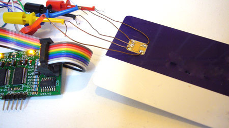
So the real hackers connect the cards:
')
The interface is the synchronous mode of the USART driver, which means that we synchronize the transmission of each bit of information with the frequency at the CLK pin, but there is one important difference from other synchronous interfaces (like the same SPI ): to clock one bit of information CLK , and 372 pulses (this magic number is written in 3 parts of ISO7816 , and is called ETU (Elementary Time Unit)), i.e., one data bit is clocked by every 372-m (ideally) front. The frequency itself should be in the range from 1 to 5 MHz.
Now let's deal with the data line ( I / O ). As I said, this is a regular UART with the following parameters:
In principle, nothing more about the hardware properties of this interface, we do not need to know. So go to the driver settings.
Here at once I will throw a piece of the initialization code written on the Standard Peripheral Library :
Here I would like to focus on two points (predecessor and rate of exchange). The point here is what? On the one hand, you need to set the speed to 9600, and on the other, the frequency that is a multiple of the system speed.
Perhaps, in most cases, if ultra-low power consumption is not required, the system frequency is selected as the maximum (in my case it is 168 MHz), the USART module I use is clocked from the APB2 bus, the maximum frequency of which is 84 MHz, then the frequency we choose should fall in the range from 1 to 5 MHz and be a multiple of 84 MHz, but for the speed of 9600 the frequency will be 9600 * 372 = 3.5712 MHz. How to be here? The developers of the standard have foreseen this moment and laid down a possible deviation from nominal values up to 20%, so, we can safely round off the frequency, say, to 3.5 MHz and choose a speed of 3,500,000 / 372 = 9409, the discrepancy here will be less than 2% that is quite acceptable. We must divide the value of the prescaler by 2, since it is set in steps of 2 (i.e., the value 1 corresponds to division by 2, 2 by 4, 3 by 6, etc.). We have (84 / 3,5) / 2 = 12:
Further, what I would like to highlight is parity error handling. To do this, there is a specially provided time interval, which is called Guard Time (we have it 16 bits). What is Guard Time ? Guard Time is the time interval during which the receiver must set a low level on the I / O line in case of a parity error ( NACK ), to which the transmitter must send the same frame again. I will not particularly argue about the usefulness of this feature, although, purely my opinion, if such errors, in principle, take place, the exchange channel can be considered unreliable, and such measures are unlikely to help here.
With the driver setup, I think, everything is clear, therefore, we proceed to the process of initiating the exchange with the card.
To start the card you need to perform a "cold" reset. It represents the following sequence:
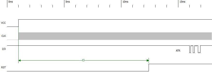
It's simple, perform a reset, waiting for a response. If the first bit of the response does not arrive within 40,000 cycles (t3), you must set the RST low level and deactivate I / O and CLK .
What is this response? ATR (Answer-to-Reset) is the following structure (the size of each field is 1 byte):
1. TS - initiating byte . It can take one of two values: 3Fh and 3Bh:
2. T0 - format byte . It consists of 2 octets:
3. TA1 . Contains parameters for frequency control:
4. TB1 . Contains VPP output characteristics:
5. TC1 . It contains the N parameter — an additional Guard Time increment (specified in ETU units); it can take a value from 0 to 254; a value of 255 indicates that the interval between the first edges of two adjacent frames is shortened to 11 ETU .
6. TD1 . There is a little confusion here, since ISO7816 does not reveal the structure of this byte, but the source [1] is pretty cleverly written. It consists of 2 octets:
7. TA2 . Contains only one significant bit (most significant), it indicates the possibility of switching to another version of the protocol (0 - switching is possible, 1 - switching is not possible), if a byte is not transmitted, it is considered to be 0
8. T1, ..., TK - historical bytes . Contain information about the card, by whom, when it is released, etc., the format of this field is not regulated by the standard
9. TCK - checksum byte . Calculated by adding modulo 2 (xor) all previous bytes (present only in the T1 protocol)
Now let's try to figure out what is needed here. We are most interested in the fields TA1 and TA2 , they indicate to us what actions we should take, namely, choose one of two modes:
If the high bit of TA2 = 0, then we use the “negotiation” mode, otherwise, the specified mode.
The negotiation exchange is a process called PTS (Protocol Type Selection). This process consists in sending a sequence by the device, which tells the card that it is ready to apply the new settings. In turn, the card must respond with the same sequence, after which both the card and the interface device can begin to work with the new settings. About what settings to apply, we are told byte TA1 frame ATR . The parameters Fi and Di are not the values themselves, but the numbers in the table. According to the table, we can find the values of F (Clock rate conversion factor) and D (Bit rate adjustment adjustment factor) corresponding to these numbers:
Fi-F table.
Table Di-D.
* RFU - reserved for future use.
The quotient of F and D is the new value of ETU , i.e. we can choose any frequency and speed, but taking into account that the ratio between them should be equal to the particular F / D.
Now more about the PTS frame itself:
1. PTSS - initiating byte (always FFh)
2. PTS0 - format byte . Defines which fields are present in the frame, the high-order octet is the bit mask:
3. PTS1 . Contains the requested values of Fi and Di , received in the TA1 ATR byte, if the byte is not transmitted, then Fi and Di are considered to be equal to 1.
4. PTS2 . Indicates whether the N parameter specified in the TC1 ATR will be applied .
5. PTS3 . Reserved.
6. PCK - checksum byte . Calculated by adding modulo 2 (xor) all previous bytes.
Everything is simple, we form a sequence, we send, we wait for the answer, we compare, if it coincides, we change the speed to Fclk / ( F / D ).
If the card does not support the "negotiation" mode, simply continue the work.
To consolidate the material try to make out a simple example. This is the usual Beeline Simka. Here is the ATR that she throws out:
The PTS frame, in this case, will look like this:
In my article, I omitted some details related, for example, by programming smart cards, and also did not consider the protocols of the channel and application levels, but there are several reasons for this. Firstly, each of these points draws on a separate article, if not more, and secondly, in my opinion, there is plenty of information on the APDU protocol on the Internet.
Well, I really hope that my work will not go unheeded, or at least satisfy the curiosity of the suffering. Anyway, thanks to everyone who has mastered, I will be happy to answer questions, and get a couple of other kicks for jambs. Finally, I strongly advise everyone to read a wonderful series of articles on cryptographic Java-cards . All good!
At once I will make a reservation that we are talking about a processor with hardware support for ISO7816 (for example, STM32F4xx ), writing a software emulator is another kind of maniae that takes place either if it is very tight, or if there is too much free time.
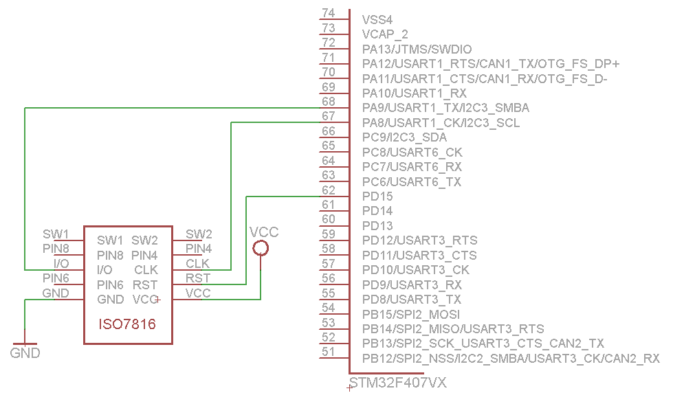
CONCLUSIONS AND WIRING DIAGRAM
So what do we have at the entrance? A 3-volt power stone and an ISO7816-2 format card , like this:
- VCC - food
- RST - reset input
- I / O - bidirectional data line
- CLK - clocking
- GND - land
- VPP - programming output
There are 3 options for VCC input: 1.8 V, 3 V, 5 V (card classes A, B, C, respectively), RST serves to reset the state machine of the card (active level is low), I / O is the data line, which is a normal UART , CLK is used to clock the processor of the card (if the card is in an inactive state, the frequency is not needed, respectively), VPP output is used to program the card.
So the real hackers connect the cards:
')
INTERFACE
The interface is the synchronous mode of the USART driver, which means that we synchronize the transmission of each bit of information with the frequency at the CLK pin, but there is one important difference from other synchronous interfaces (like the same SPI ): to clock one bit of information CLK , and 372 pulses (this magic number is written in 3 parts of ISO7816 , and is called ETU (Elementary Time Unit)), i.e., one data bit is clocked by every 372-m (ideally) front. The frequency itself should be in the range from 1 to 5 MHz.
Now let's deal with the data line ( I / O ). As I said, this is a regular UART with the following parameters:
- Data bit: 8
- Stop bit: 1.5
- Par Bit: Even
- Speed (at the start): 9600 Baud
In principle, nothing more about the hardware properties of this interface, we do not need to know. So go to the driver settings.
DRIVER SETUP
Here at once I will throw a piece of the initialization code written on the Standard Peripheral Library :
RCC_ClocksTypeDef RCC_Clocks; USART_InitTypeDef USART_InitStructure; USART_ClockInitTypeDef USART_ClockInitStructure; NVIC_InitTypeDef NVIC_InitStructure; /// RCC_GetClocksFreq(&RCC_Clocks); /// SC_USART_APB_PERIPH_CLOCK(RCC_APB2Periph_USART1, ENABLE); /// USART_SetPrescaler(USART1, (RCC_Clocks.PCLK2_Frequency / CLK_FREQ) / 2); /// Guard Time USART_SetGuardTime(USART1, 16); /// ( CLK) USART_ClockInitStructure.USART_Clock = USART_Clock_Enable; USART_ClockInitStructure.USART_CPOL = USART_CPOL_Low; USART_ClockInitStructure.USART_CPHA = USART_CPHA_1Edge; USART_ClockInitStructure.USART_LastBit = USART_LastBit_Enable; USART_ClockInit(USART1, &USART_ClockInitStructure); /// ( I/O) USART_InitStructure.USART_BaudRate = CLK_FREQ / ETU; USART_InitStructure.USART_WordLength = USART_WordLength_9b; USART_InitStructure.USART_StopBits = USART_StopBits_1_5; USART_InitStructure.USART_Parity = USART_Parity_Even; USART_InitStructure.USART_Mode = USART_Mode_Rx | USART_Mode_Tx; USART_InitStructure.USART_HardwareFlowControl = USART_HardwareFlowControl_None; USART_Init(USART1, &USART_InitStructure); /// NACK USART_SmartCardNACKCmd(USART1, ENABLE); /// - USART_SmartCardCmd(USART1, ENABLE); /// USART_Cmd(USART1, ENABLE); /// 2 ( ) USART_ITConfig(USART1, USART_IT_RXNE, ENABLE); USART_ITConfig(USART1, USART_IT_PE, ENABLE); /// NVIC_InitStructure.NVIC_IRQChannel = USART1_IRQn; NVIC_InitStructure.NVIC_IRQChannelPreemptionPriority = 0; NVIC_InitStructure.NVIC_IRQChannelSubPriority = 0; NVIC_InitStructure.NVIC_IRQChannelCmd = ENABLE; NVIC_Init(&NVIC_InitStructure); I lowered the output settings so as not to clutter up with code, but here there is one important point: the I / O output should be configured as Open-Drain , since the standard provides for the possibility of finding the line in the Z-state, when the card decides where to pull it.
Here I would like to focus on two points (predecessor and rate of exchange). The point here is what? On the one hand, you need to set the speed to 9600, and on the other, the frequency that is a multiple of the system speed.
Perhaps, in most cases, if ultra-low power consumption is not required, the system frequency is selected as the maximum (in my case it is 168 MHz), the USART module I use is clocked from the APB2 bus, the maximum frequency of which is 84 MHz, then the frequency we choose should fall in the range from 1 to 5 MHz and be a multiple of 84 MHz, but for the speed of 9600 the frequency will be 9600 * 372 = 3.5712 MHz. How to be here? The developers of the standard have foreseen this moment and laid down a possible deviation from nominal values up to 20%, so, we can safely round off the frequency, say, to 3.5 MHz and choose a speed of 3,500,000 / 372 = 9409, the discrepancy here will be less than 2% that is quite acceptable. We must divide the value of the prescaler by 2, since it is set in steps of 2 (i.e., the value 1 corresponds to division by 2, 2 by 4, 3 by 6, etc.). We have (84 / 3,5) / 2 = 12:
- Frequency ( CLK ): 3.5 MHz
- Speed ( I / O ): 9409 Baud
- Presclaer: 12
Further, what I would like to highlight is parity error handling. To do this, there is a specially provided time interval, which is called Guard Time (we have it 16 bits). What is Guard Time ? Guard Time is the time interval during which the receiver must set a low level on the I / O line in case of a parity error ( NACK ), to which the transmitter must send the same frame again. I will not particularly argue about the usefulness of this feature, although, purely my opinion, if such errors, in principle, take place, the exchange channel can be considered unreliable, and such measures are unlikely to help here.
With the driver setup, I think, everything is clear, therefore, we proceed to the process of initiating the exchange with the card.
START
To start the card you need to perform a "cold" reset. It represents the following sequence:
- Set RST low
- Power on VCC
- Apply CLK frequency
- Wait a time interval equal to 40000 CLK cycles
- Set high on RST
- Wait a response for 40,000 cycles
It's simple, perform a reset, waiting for a response. If the first bit of the response does not arrive within 40,000 cycles (t3), you must set the RST low level and deactivate I / O and CLK .
ATR
What is this response? ATR (Answer-to-Reset) is the following structure (the size of each field is 1 byte):
- TS: Initial character
- TO: Format character
- TAi: Interface character [codes FI, DI]
- TBi: Interface character [codes II, PI1]
- TCi: Interface character [codes N]
- TDi: Interface character [codes Yi + 1, T]
- T1, ..., TK: Historical characters (max, 15)
- TCK: Check character
1. TS - initiating byte . It can take one of two values: 3Fh and 3Bh:
- 3Fh - Inverse Convention - inverse polarity, i.e. 0 is transmitted high, and 1 is low (important point, odd, i.e., odd) will be used here to control parity:
- 3Bh - Direct Convention - direct polarity - the same, but exactly the opposite (parity - even, i.e., even)
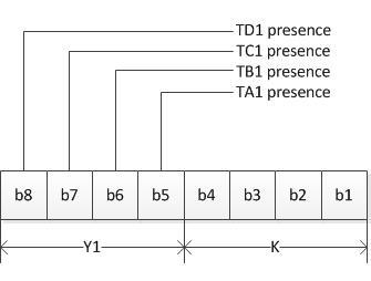
2. T0 - format byte . It consists of 2 octets:
- Y1 (most significant octet) is a bitmask that indicates which fields follow:
- b5 - TA1 is transmitted
- b6 - TB1 is transmitted
- b7 - TC1 is transmitted
- b8 - TD1 is transmitted
- K (low octet) - the number of "historical" bytes
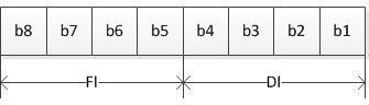
3. TA1 . Contains parameters for frequency control:
- FI (senior octet) - divisible
- DI (low octet) - divider
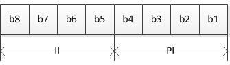
4. TB1 . Contains VPP output characteristics:
- II (bits b7 - b6) - maximum programming current
- PI (bits b5 - b1) - programming voltage
5. TC1 . It contains the N parameter — an additional Guard Time increment (specified in ETU units); it can take a value from 0 to 254; a value of 255 indicates that the interval between the first edges of two adjacent frames is shortened to 11 ETU .
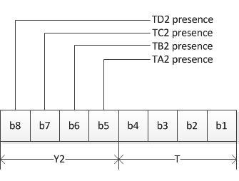
6. TD1 . There is a little confusion here, since ISO7816 does not reveal the structure of this byte, but the source [1] is pretty cleverly written. It consists of 2 octets:
- Y2 (high-order octet) is a bitmask that indicates which fields follow:
- b5 - TA2 is transmitted
- b6 - TB2 is transmitted
- b7 - TC2 transmitted
- b8 - TD2 is transmitted
- T (low octet) - used protocol (0 - T0, 1 - T1, other values are reserved)
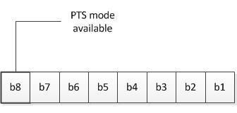
7. TA2 . Contains only one significant bit (most significant), it indicates the possibility of switching to another version of the protocol (0 - switching is possible, 1 - switching is not possible), if a byte is not transmitted, it is considered to be 0
8. T1, ..., TK - historical bytes . Contain information about the card, by whom, when it is released, etc., the format of this field is not regulated by the standard
9. TCK - checksum byte . Calculated by adding modulo 2 (xor) all previous bytes (present only in the T1 protocol)
Now let's try to figure out what is needed here. We are most interested in the fields TA1 and TA2 , they indicate to us what actions we should take, namely, choose one of two modes:
- Negotiation mode
- Specified mode (specific mode)
If the high bit of TA2 = 0, then we use the “negotiation” mode, otherwise, the specified mode.
PTS
The negotiation exchange is a process called PTS (Protocol Type Selection). This process consists in sending a sequence by the device, which tells the card that it is ready to apply the new settings. In turn, the card must respond with the same sequence, after which both the card and the interface device can begin to work with the new settings. About what settings to apply, we are told byte TA1 frame ATR . The parameters Fi and Di are not the values themselves, but the numbers in the table. According to the table, we can find the values of F (Clock rate conversion factor) and D (Bit rate adjustment adjustment factor) corresponding to these numbers:
Fi-F table.
| FI | 0000 | 0001 | 0010 | 0011 | 0100 | 0101 | 0110 | 0111 |
| F | internal clk | 372 | 558 | 744 | 1116 | 1488 | 1860 | RFU |
| FI | 1000 | 1001 | 1010 | 1011 | 1100 | 1101 | 1110 | 1111 |
| F | RFU | 512 | 768 | 1024 | 1536 | 2048 | RFU | RFU |
Table Di-D.
| DI | 0000 | 0001 | 0010 | 0011 | 0100 | 0101 | 0110 | 0111 |
| D | RFU | one | 2 | four | eight | sixteen | RFU | RFU |
| DI | 1000 | 1001 | 1010 | 1011 | 1100 | 1101 | 1110 | 1111 |
| D | RFU | RFU | 1/2 | 1/4 | 1/8 | 1/16 | 1/32 | 1/64 |
* RFU - reserved for future use.
The quotient of F and D is the new value of ETU , i.e. we can choose any frequency and speed, but taking into account that the ratio between them should be equal to the particular F / D.
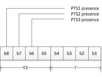
Now more about the PTS frame itself:
- PTSS: Initial character (Mandatory)
- PTS0: Format character (Mandatory)
- PTS1 (Optional)
- PTS2 (Optional)
- PTS3 (Optional)
- PCK: Check character (Mandatory)
1. PTSS - initiating byte (always FFh)
2. PTS0 - format byte . Defines which fields are present in the frame, the high-order octet is the bit mask:
- b5 - PTS1 transmitted
- b6 - PTS2 transmitted
- b7 - PTS3 transmitted
- b8 - always 0, reserved
- T (low octet) - used protocol (0 - T0, 1 - T1, other values are reserved)
3. PTS1 . Contains the requested values of Fi and Di , received in the TA1 ATR byte, if the byte is not transmitted, then Fi and Di are considered to be equal to 1.
4. PTS2 . Indicates whether the N parameter specified in the TC1 ATR will be applied .
5. PTS3 . Reserved.
6. PCK - checksum byte . Calculated by adding modulo 2 (xor) all previous bytes.
Everything is simple, we form a sequence, we send, we wait for the answer, we compare, if it coincides, we change the speed to Fclk / ( F / D ).
If the card does not support the "negotiation" mode, simply continue the work.
EXAMPLE
To consolidate the material try to make out a simple example. This is the usual Beeline Simka. Here is the ATR that she throws out:
 3B 3B 94 00 9B 44 20 10 4D AD 40 00 33 90 00
 3Bh (TS) - direct convention
 3Bh (T0) (0011 1011) - we expect TA1 and TB1, the number of "historical" bytes = 11
 94h (TA1) - Fi = 9, Di = 4, we find F and D according to tables 1 and 2 (F = 512, D = 8), the new ETU = 512/8 = 64
 00h (TB1) - VPP is not supported
The PTS frame, in this case, will look like this:
 FF 10 94 7B
 FFh (PTSS) - initiating byte
 10h (PTS0) (0001 0000) - transmit PTS0, T0 protocol
 94h (PTS1) = TA1
 7Bh (PCK) = xor (FF 10 94)
CONCLUSION
In my article, I omitted some details related, for example, by programming smart cards, and also did not consider the protocols of the channel and application levels, but there are several reasons for this. Firstly, each of these points draws on a separate article, if not more, and secondly, in my opinion, there is plenty of information on the APDU protocol on the Internet.
Well, I really hope that my work will not go unheeded, or at least satisfy the curiosity of the suffering. Anyway, thanks to everyone who has mastered, I will be happy to answer questions, and get a couple of other kicks for jambs. Finally, I strongly advise everyone to read a wonderful series of articles on cryptographic Java-cards . All good!
LINKS
- http://www.cardwerk.com/smartcards/smartcard_standard_ISO7816.aspx - Sobsno, the standard itself
- http://www.hackersrussia.ru/Cards/ASyncro/ISO7816-3.php ISO7816 in Russian
- http://www.st.com/web/en/resource/technical/document/application_note/CD00166510.pdf - Application Note for STM32F10x
- http://www.smartcard.co.uk/tutorials/sct-itsc.pdf - Nice Smart Card Tutorial
Source: https://habr.com/ru/post/257279/
All Articles