WS2812B protocol on STM32 without empty loops and interrupts. And how to make the right rainbow
On Habré there are already a couple of articles about working with RGB LEDs WS2112B, but for some reason they all use a rather archaic way to form a bit sequence. The method consists in forming exact time intervals using empty program cycles. Perhaps this is the cost of using the Arduino, but we, of course, have long since switched to ARM Cortex-M4 in the face of STM32 and can afford to make it more beautiful.
So, I recall the "protocol" WS2112B.
')
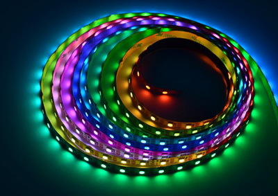
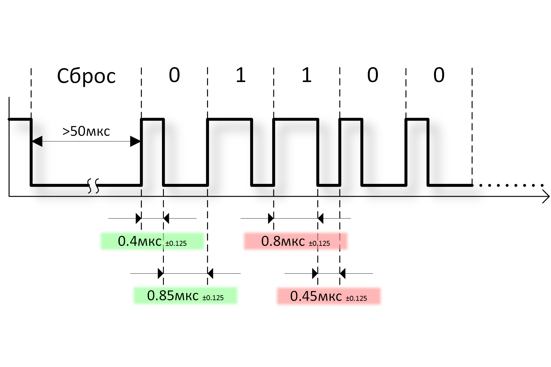
The LED strip on the WS2112B has only one digital input - DIN, connected to the first LED on the strip. A special pulse sequence encoding the bits is applied to it, as shown in the figure. Each LED has one digital output - DOUT connected to the DIN input of the next LED on the bar. Each LED needs to transmit 24 bits (8 bits for each color: red R, green G and blue B). Thus, in order to light all the LEDs, 24 * N bits must be transmitted, where N is the number of LEDs on the strip.
Having accepted the bits, the LEDs light up and statically light until they receive a new bit sequence. Each bit sequence begins with the installation of DIN in the log. zero for at least 50 µs.
As you can see, the bits are encoded with rather short pulses with tight tolerances. A microcontroller trying to generate them with software delays is required at least to disable all interrupts so that, by chance, a reset or a failed bit is not formed. CPU time resources here are also wasted irrationally, in order to light 100 LEDs the processor needs to work 3 ms. If you update the state of the LEDs with a frequency of 100 Hz, then this "protocol" will take 30% of the processor time.
There are suggestions to use the SPI interface to transmit a bitstream to the WS2112B. But here an obstacle can be the insufficient correspondence of the clock frequency of the system bus and the strong errors of the pulse durations.
Meanwhile, in STM32 and in general, all Cortex-M chips have an excellent Direct Memory Access (DMA) mechanism. Bits can be generated using timers in pulse-width modulation mode, and each subsequent bit can be extracted from RAM using DMA.
The figure below shows the scheme of interaction between DMA and timer TIM4 in the STM32F407VET6 chip. Debugging was carried out on my industrial controller with just such a chip, but with the same success, everything can be repeated on any chip of the STM32 family. In this case, it was my conclusion that 8 GPIOB was free, which I used.

Further, the initialization text of the timer and controller:
#define BIT(n) (1u << n) #define LSHIFT(v,n) (((unsigned int)(v) << n)) #define LEDS_NUM 80 #define COLRS 3 INT16U DMA_buf[LEDS_NUM+2][COLRS][8]; /*------------------------------------------------------------------------------ Timer4 PCLK1 72 MHz 3 Compare DMA CCR3 ------------------------------------------------------------------------------*/ void Timer4_init(void) { TIM_TypeDef *tim = TIM4; RCC_TypeDef *rcc = RCC; rcc->APB1RSTR |= BIT(2); // 4 rcc->APB1RSTR &= ~BIT(2); rcc->APB1ENR |= BIT(2); // 4 tim->CR1 = BIT(7); // 1: TIMx_ARR register is buffered. tim->CR2 = 0; tim->PSC = 0; // 72 tim->ARR = 90 - 1; // 1.25 tim->CCMR2 = 0 + LSHIFT(6, 4) // OC3M: Output compare 3 mode | 110: PWM mode 1 - In upcounting, channel 1 is active as long as TIMx_CNT<TIMx_CCR1 else inactive. + LSHIFT(1, 3) // OC3PE: Output compare 3 preload enable + LSHIFT(0, 0) // CC3S: Capture/Compare 3 selection | 00: CC3 channel is configured as output ; tim->CNT = 0; tim->CCR3 = 0; tim->DIER = BIT(11); // Bit 11 CC3DE: Capture/Compare 3 DMA request enable. DMA tim->CR1 |= BIT(0); // tim->CCER = BIT(8); // , DMA } /*------------------------------------------------------------------------------ 2 DMA1 Stream 7 WS2812B TMR4 PWM ------------------------------------------------------------------------------*/ void DMA1_Stream7_Mem_to_TMR4_init(void) { DMA_Stream_TypeDef *dma_ch = DMA1_Stream7; RCC_TypeDef *rcc = RCC; rcc->AHB1ENR |= BIT(21); // DMA1 dma_ch->CR = 0; // dma_ch->PAR = (unsigned int)&(TIM4->CCR3) + 1; // ADC dma_ch->M0AR = (unsigned long)&DMA_buf; dma_ch->NDTR = (LEDS_NUM + 2) * COLRS * 8; dma_ch->CR = LSHIFT(2, 25) + // CHSEL[2:0]: Channel selection | 010: channel 2 selected LSHIFT(0, 23) + // MBURST: Memory burst transfer configuration | 00: single transfer LSHIFT(0, 21) + // PBURST[1:0]: Peripheral burst transfer configuration | 00: single transfer LSHIFT(0, 19) + // CT: Current target (only in double buffer mode) | 0: The current target memory is Memory 0 (addressed by the DMA_SxM0AR pointer) LSHIFT(0, 18) + // DBM: Double buffer mode | 0: No buffer switching at the end of transfer LSHIFT(3, 16) + // PL[1:0]: Priority level | 11: Very high. PL[1:0]: Priority level LSHIFT(0, 15) + // PINCOS: Peripheral increment offset size | 0: The offset size for the peripheral address calculation is linked to the PSIZE LSHIFT(1, 13) + // MSIZE[1:0]: Memory data size | 00: 8-bit. Memory data size LSHIFT(1, 11) + // PSIZE[1:0]: Peripheral data size | 00: 8-bit. Peripheral data size LSHIFT(1, 10) + // MINC: Memory increment mode | 1: Memory address pointer is incremented after each data transfer (increment is done according to MSIZE) LSHIFT(0, 9) + // PINC: Peripheral increment mode | 0: Peripheral address pointer is fixed LSHIFT(1, 8) + // CIRC: Circular mode | 1: Circular mode enabled LSHIFT(1, 6) + // DIR[1:0]: Data transfer direction | 01: Memory-to-peripheral LSHIFT(0, 5) + // PFCTRL: Peripheral flow controller | 1: The peripheral is the flow controller LSHIFT(1, 4) + // TCIE: Transfer complete interrupt enable | 1: TC interrupt enabled LSHIFT(0, 3) + // HTIE: Half transfer interrupt enable | 0: HT interrupt disabled LSHIFT(0, 2) + // TEIE: Transfer error interrupt enable | 0 : TE interrupt disabled LSHIFT(0, 1) + // DMEIE: Direct mode error interrupt enable | 0: Direct mode error interrupt disabled LSHIFT(0, 0) + // EN: Stream enable | 1: Stream enabled 0; dma_ch->FCR = LSHIFT(0, 7) + // FEIE: FIFO error interrupt enable LSHIFT(1, 2) + // DMDIS: Direct mode disable | 1: Direct mode disabled. LSHIFT(1, 0) + // FTH[1:0]: FIFO threshold selection | 01: 1/2 full FIFO 0; dma_ch->CR |= BIT(0); // 1: Stream enabled } After this initialization, the automatic transfer of the bitstream from the DMA_buf array located in RAM to the external output 8 GPIOB begins. Automatically generated and 50 microsecond reset pause. The processor is not involved in the transfer, not even interrupts are used. To light any LED, you just need to write the corresponding word in the array DMA_buf at the appropriate offset. This is done in the project by the function LEDstrip_set_led_state.
This is not to say that this mechanism does not affect the processor at all. His work slows down somewhat. Because it shares with DMA shared access to RAM and system bus. But measurements have shown that this slowdown does not exceed 0.2% in this case.
The MDK-ARM Professional Version: 4.72.1.0 development environment was used to write the project. The processor frequency is 144 MHz, the PCLK1 frequency is 72 MHz. Easily transferred to the STM32 MCU Discovery Kits. The whole project is laid out here.
The project did not use libraries from ST or any other third-party libraries. The project is very compact, everything is written through direct access to the registers, it makes the text shorter, clearer and makes it easier to transfer to other development environments.
And about the rainbow
The fact is that simply linearly incrementing the bytes in a word in the RGB color format (bit representation - 00000000 RRRRRRRR GGGGGGGG BBBBBBBB) cannot be depicted on a LED strip with a hundred LEDs to draw a beautiful rainbow. It is even more difficult for this rainbow to adjust the brightness, making simple manipulations on a 32-bit word with RGB information. For such manipulations use HSV format. For example, the entire rainbow will be represented by simply linearly incrementing the H-component. Then convert HSV to RGB and output to LEDs.
There are two HSV to RGB converters in the project, one is integer and the other is using floating point calculations. Visually, I did not see the differences. Yes, unfortunately, there is no place for STM32 here.
Source: https://habr.com/ru/post/257131/
All Articles