Using the driver keys of the lower and upper levels of the IR2110 - an explanation and examples of schemes
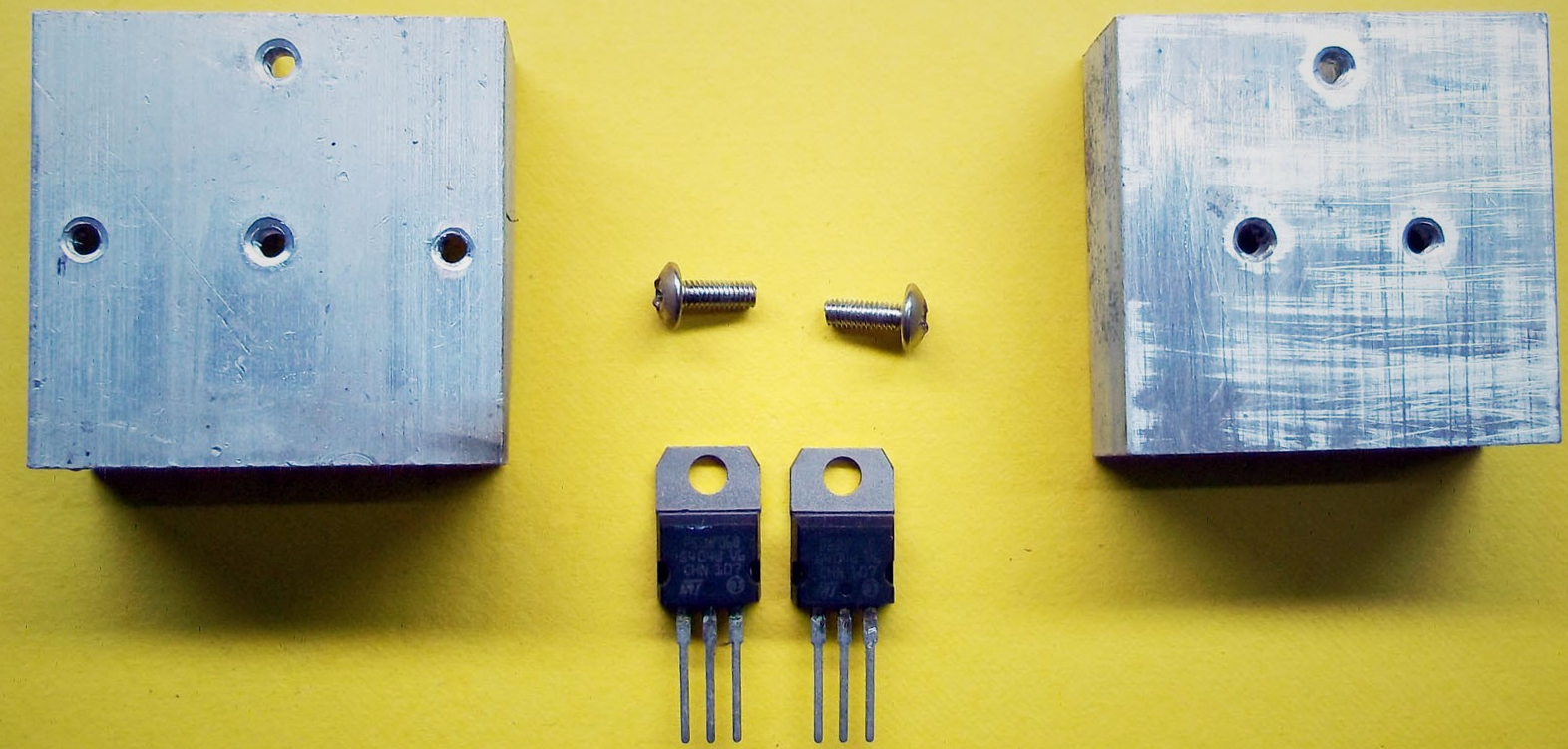
Perhaps, after reading this article, you will not have to put radiators of the same size on transistors.
Translation of this article .
A small appeal from the translator:
Firstly, in this translation there can be serious problems with the translation of terms, I have not done electrical engineering and circuit engineering enough, but I still know something; I also tried to translate everything as clear as possible, so I didn’t use such concepts as a bootstrap, MOS transistor, etc. Secondly, if spelling is now difficult to make a mistake (praise to word processors with an indication of errors), then a mistake in punctuation is quite simple to make.
And on these two points, please kick me in the comments as much as possible.
Now let's talk more about the topic of the article - with all the variety of articles on the construction of various ground-based vehicles (typewriters) on the MK, on the Arduino, on <insert name>, the design of the circuit itself, and even more, the motor connection scheme is not described in sufficient detail. Usually it looks like this:
- we take the engine
- we take components
- we connect components and the engine
- ...
- PROFIT! 1!
')
But for building more complex circuits than for simple torsion of a motor with PWM in one direction through L239x, you usually need knowledge about full bridges (or H-bridges), field-effect transistors (or MOSFET), and of drivers for them. If nothing limits, then p-channel and n-channel transistors can be used for a full bridge, but if the motor is powerful enough, then p-channel transistors will have to be hung with a large number of radiators first, then coolers should be added, but if you really throw them out, then you can try other types of cooling, or just use only n-channel transistors in the circuit. But with n-channel transistors there is a small problem - sometimes it is quite difficult to open them “in an amicable way”.
Therefore, I was looking for something that would help me with drawing up the correct scheme, and I found an article in a blog of a young man, whose name is Syed Tahmid Mahbub. I decided to share this article.
In many situations, we have to use field-effect transistors as top-level switches. Also in many situations we have to use field-effect transistors as the keys of both the upper and lower levels. For example, in bridge circuits. In incomplete bridges we have 1 upper level MOSFET and 1 lower level MOSFET. In complete bridge circuits, we have 2 upper level MOSFETs and 2 lower level MOSFETs. In such situations, we will need to use both high and low level drivers together. The most common way to control field effect transistors in such cases is to use a low and high level key driver for the MOSFET. Undoubtedly, the most popular driver IC is the IR2110. And in this article / tutorial, I will talk about it about him.
You can download the documentation for the IR2110 from the IR site. Here is the download link: http://www.irf.com/product-info/datasheets/data/ir2110.pdf
Let's first take a look at the block diagram, as well as the description and location of contacts:
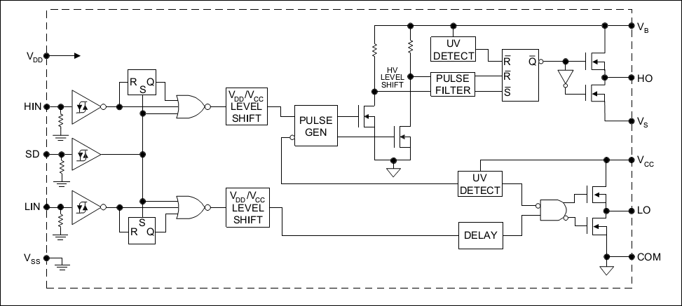
Figure 1 - Functional block diagram of the IR2110
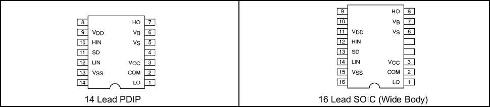
Figure 2 - IR2110 pinout
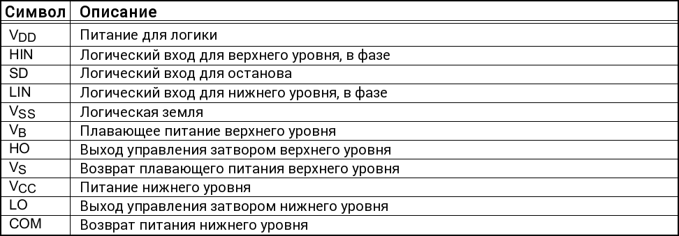
Figure 3 - Description of pins IR2110
It is also worth mentioning that the IR2110 is available in two packages - in the form of a 14-pin PDIP for terminal installation and a 16-pin SOIC for surface mounting.
Now let's talk about the various contacts.
VCC is a low power supply, it should be between 10V and 20V. VDD is a logical power supply for the IR2110, it should be between + 3V and + 20V (relative to VSS). The actual voltage you choose to use depends on the voltage level of the input signals. Here is the schedule:
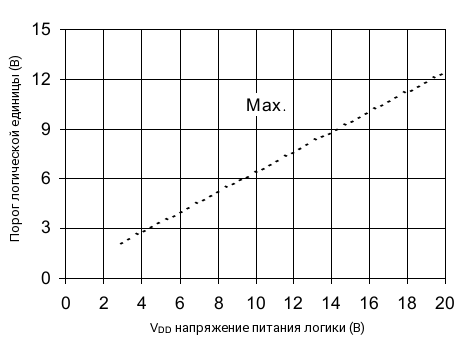
Figure 4 - Dependence of logical 1 on power
A commonly used VDD of + 5V. When VDD = + 5V, the input threshold of logical 1 is slightly higher than 3V. Thus, when the voltage VDD = + 5V, the IR2110 can be used to control the load when the input “1” is higher than 3 (some) volts. This means that the IR2110 can be used for almost all circuits, since most circuits usually have approximately 5V power. When you use microcontrollers, the output voltage will be higher than 4V (because the microcontroller often has VDD = + 5V). When using SG3525 or TL494 or another PWM controller, you will probably have to supply them with a voltage greater than 10V, which means that the outputs will be greater than 8V, with a logical one. Thus, IR2110 can be used almost everywhere.
You can also reduce the VDD to about + 4V if you use a microcontroller or any chip that produces 3.3V at the output (for example, dsPIC33). When designing circuits with the IR2110, I noticed that sometimes the circuit does not work properly when the VDD of the IR2110 was selected to be less than + 4V. Therefore, I do not recommend using VDD below + 4V. In most of my circuits, signal levels do not have a voltage less than 4V as "1", and therefore I use VDD = + 5V.
If for any reason in the circuit the signal level of the logical "1" has a voltage less than 3V, then you need to use a level converter / level translator, it will raise the voltage to acceptable limits. In such situations, I recommend raising to 4V or 5B and using IR2110 VDD = + 5V.
Now let's talk about VSS and COM. VSS is a land for logic. COM is a “low return” - basically a low-level driver ground. It may look like they are independent, and you might think that it would probably be possible to isolate the driver outputs and the driver signal logic. However, that would be wrong. Although not internally connected, the IR2110 is a non-isolated driver, which means that VSS and COM must both be connected to ground.
HIN and LIN are logical inputs. A high HIN signal means that we want to control the upper key, that is, the HO output is high. A low signal on the HIN means that we want to disable the top-level MOSFET, that is, the low-level output is performed on the HO. An exit to HO, high or low, is considered not in relation to the ground, but in relation to VS. We will soon see how the amplifying circuits (diode + capacitor), using VCC, VB and VS, provide floating power to control the MOSFET. VS is a floating power return. At a high level, the level at HO is equal to the level at VB, relative to VS. At a low level, the level at HO is equal to VS, in relation to VS, is actually zero.
A high LIN signal means that we want to control the lower key, that is, a high level output is performed on the LO. A low LIN signal means that we want to disable the low-level MOSFET, that is, a low-level output is provided to the LO. An exit to the LO is relative to land. When the signal is high, the level in LO is the same as in VCC, relative to VSS, actually ground. When the signal is low, the level in LO is the same as in VSS, relative to VSS, actually zero.
SD is used as a stop control. When the level is low, the IR2110 is on - the stop function is disabled. When this pin is high, the outputs are turned off, disabling the IR2110 control.
Now let's take a look at the frequent configurations with the IR2110 for managing MOSFETs as upper and lower keys — half bridge schemes.
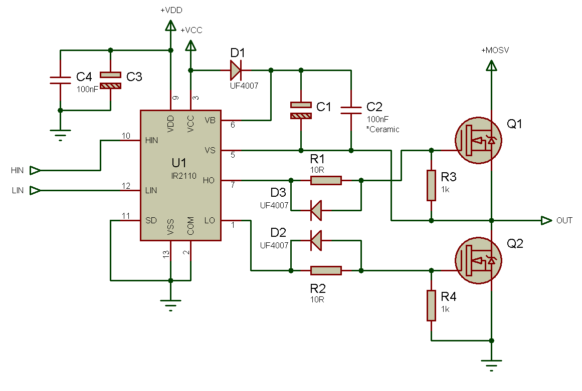
Figure 5 - Baseline on IR2110 for half-bridge control
D1, C1 and C2 together with IR2110 form an amplifying circuit. When LIN = 1 and Q2 is on, C1 and C2 are charged to the level of VB, since one diode is located below + VCC. When LIN = 0 and HIN = 1, the charge on C1 and C2 is used to add additional voltage, VB in this case, above the level of source Q1 to control Q1 in the configuration of the upper key. A sufficiently large capacity must be selected from C1 in order for it to be enough to provide the necessary charge for Q1, so that Q1 has been switched on all this time. C1 also should not have too much capacity, since the charging process will take a long time and the voltage level will not increase sufficiently to keep the MOSFET on. The more time it takes in the on state, the greater the capacity required. Thus, a lower frequency requires a greater capacity of C1. A higher fill factor requires a higher capacity C1. Of course, there are formulas for calculating the capacity, but for this you need to know a lot of parameters, and some of them we may not know, for example, the leakage current of a capacitor. Therefore, I just appreciated the approximate capacity. For low frequencies, such as 50Hz, I use a capacitance from 47µF to 68µF. For high frequencies, such as 30-50kHz, I use a capacitance from 4.7µF to 22µF. Since we use an electrolytic capacitor, the ceramic capacitor should be used in parallel with this capacitor. Ceramic capacitor is optional, if the amplifying capacitor is tantalum.
D2 and D3 discharge gate MOSFETs quickly, bypassing the gate resistors and reducing the shutdown time. R1 and R2 are current-limiting gate resistors.
+ MOSV can be a maximum of 500V.
+ VCC should come from a source without interference. You must install filtering and decoupling capacitors from + VCC to ground for filtering.
Let's now take a look at some examples of circuits with the IR2110.

Figure 6 - Diagram with IR2110 for high-voltage half-bridge
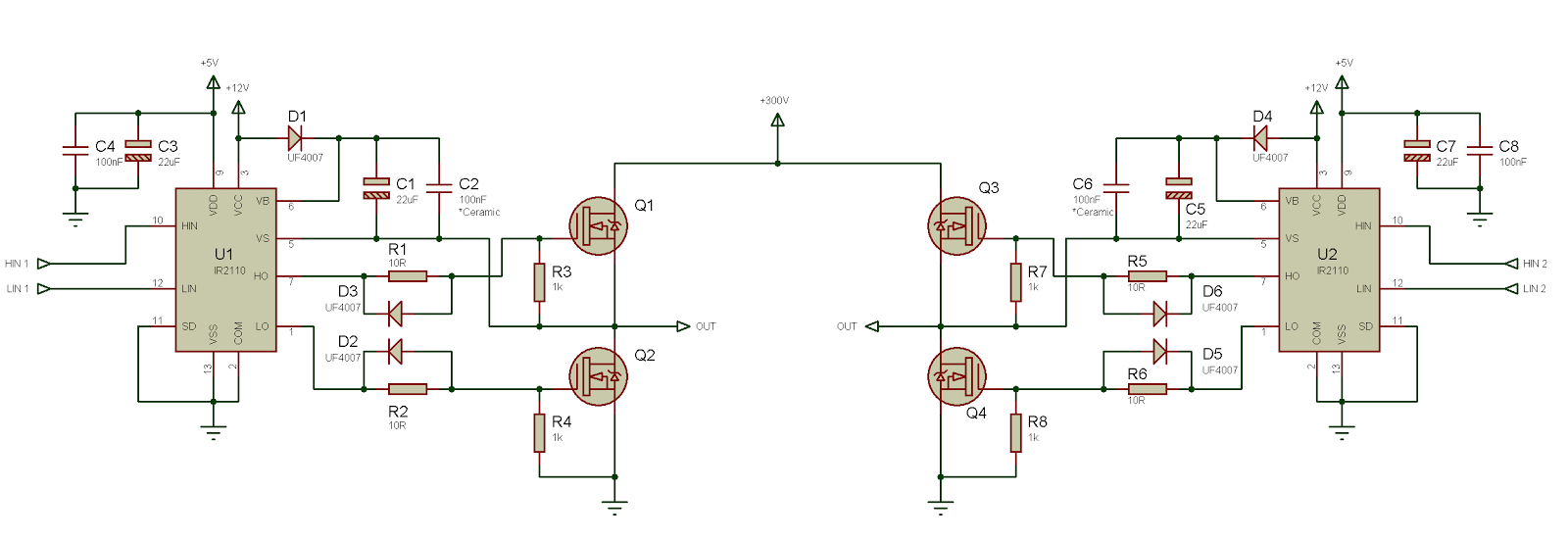
Figure 7 - Diagram with IR2110 for a high-voltage full bridge with independent key management (clickable)
In Figure 7, we see the IR2110 used to control the full bridge. There is nothing complicated in it and, I think, you already understand this now. Also here you can apply a fairly popular simplification: we connect HIN1 with LIN2, and we connect HIN2 with LIN1, thus we get control of all 4 keys using only 2 input signals, instead of 4, this is shown in Figure 8.
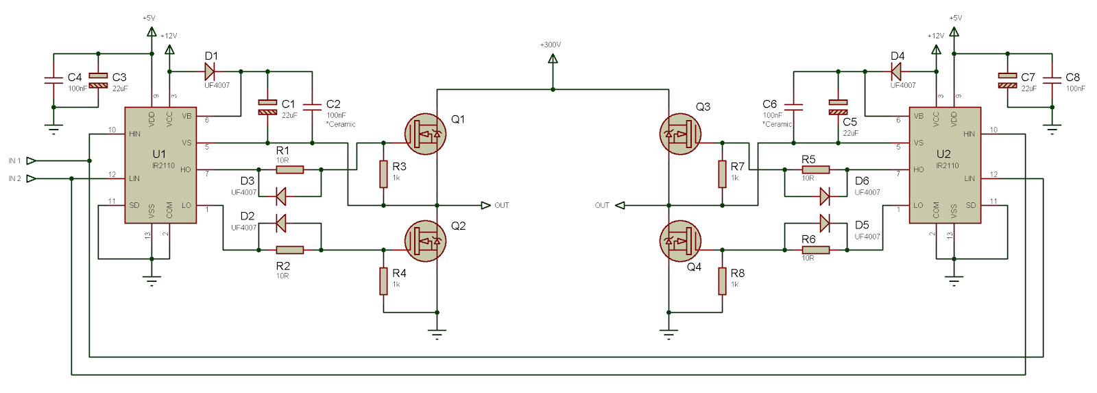
Figure 8 - Diagram with IR2110 for a high-voltage full bridge with key management with two inputs (clickable)
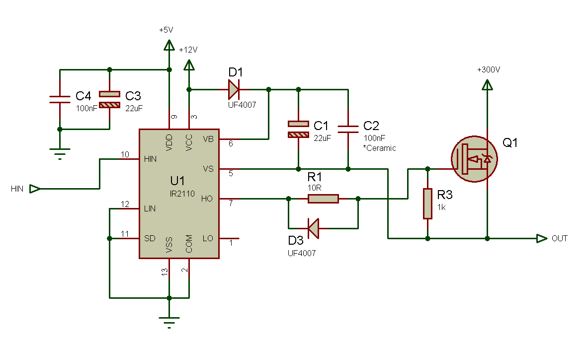
Figure 9 - Circuit with IR2110 as a high-voltage top-level driver
In Figure 9, we see the IR2110 used as the top-level driver. The scheme is quite simple and has the same functionality as described above. There is a thing to consider - since we no longer have a low-level key, there must be a load connected from OUT to the ground. Otherwise, the amplifying capacitor will not be able to charge.
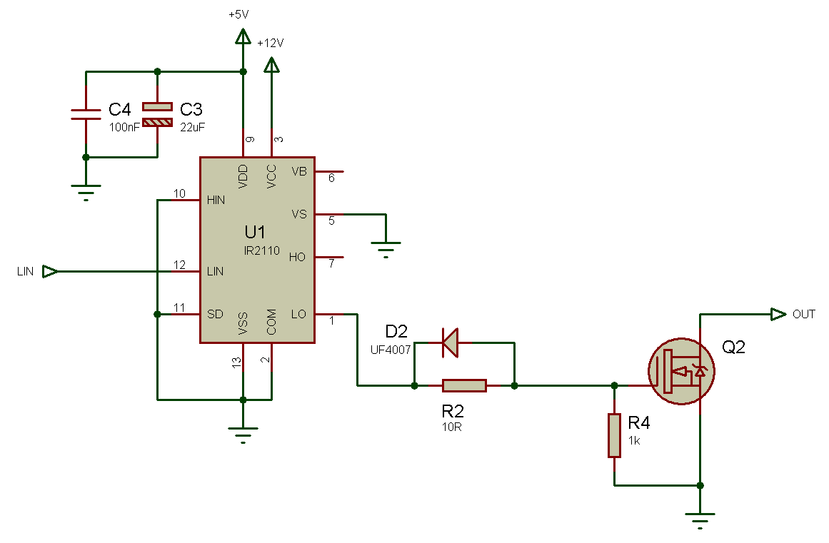
Figure 10 - Diagram with IR2110 as a low-level driver
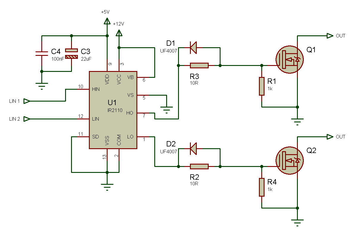
Figure 11 - Scheme with IR2110 as a dual low-level driver
If you have problems with the IR2110 and everything constantly fails, burns or explodes, then I am sure that this is due to the fact that you are not using gate-source resistors, provided, of course, that you designed everything carefully. NEVER FORGET ABOUT THE RESISTOR ON THE VALVE LOCK . If you're interested, you can read about my experience with them here (I also explain the reason why resistors prevent damage): http://tahmidmc.blogspot.com/2012/10/magic-of-knowledge.html
For further reading, I recommend this: http://www.irf.com/technical-info/appnotes/an-978.pdf
I have seen how in many forums, people are struggling with designing circuits on the IR2110. I also had a lot of difficulties before I could confidently and consistently build successful driver circuits on the IR2110. I tried to explain the application and use of the IR2110 quite thoroughly, explaining everything along the way and using a large number of examples, and I hope that this will help you in your endeavors with the IR2110.
Source: https://habr.com/ru/post/256353/
All Articles