Reverse Engineering ESP8266 - Part 1
Having succumbed to the general wave of enthusiasm for the “Smart Home” systems, as well as having a specialized education as an engineer of the automated process control systems, I am pleased to take up this topic in the form of a hobby. In this article I will share with you my experience of reverse engineering of the popular module ESP8266.
Basically, I was interested in the internal structure of SoC, the architecture and system of the processor commands, the procedure for starting and loading the firmware, and other equally interesting things. Starting the study of this module, I was faced with the fact that the necessary information on it is not much, and it is often quite contradictory. Therefore, much had to be rechecked, something to find out empirically, but something just to guess. I will be glad to your comments and additions.
To systematize all the information received, and this article was written.
')
I will not give technical specifications, a lot has been written about this, including on Habré. Those interested can be found, for example, here .
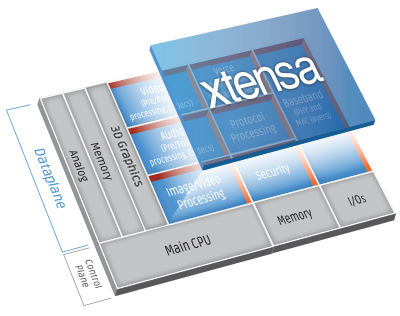
Let's start with the overall system architecture. The module is a Soc, based on the Xtensa processor family - Tensilica's L106 Diamond series manufactured by the American company Cadence , as well as a 512kB flash memory chip. The module itself was developed by the Chinese company Espressif Systems . Thus, the basic official information on ESP8266 comes from Espressif (in Chinese and in translation), and some general information can be obtained from Cadence.
A feature of this family of processors is that they are a designer, from which the customer can use the proposed Xtensa Processor Generator tool to assemble a chip with the characteristics it needs and order it from the manufacturer. Therefore, various modifications can be very different, for example, the number of cores, additional instructions, DSP modules and so on.
As I said above, the model consists of a flash ROM of 512 KB in size and SoC, which, according to unconfirmed data, has RAM up to 248 KB.
In general, all that concerns memory — the location, properties, and attributes of segments — are community searches. For some reason, this question is bypassed in the original Chinese documentation.
One of the options (there are contradictions with other sources) of the currently known memory card can be viewed here . I will cite only the most interesting addresses:
Inner memory:
Different segments of the address space can be RAM, ROM or submapped directly to flash. Podmaplennye areas are cached for speed.
Flash:
Now, before proceeding to the process of launching the module, consider the format of the firmware. To download a custom firmware, it is usually enough to write 2 data blocks: at the address 00000h and 40000h. The remaining blocks may require flashing to reset the configuration, for example, when uploading a new firmware with an incompatible data format.
A block starting with 40000h contains a simple binary code that is loaded and running unchanged. But the block, starting with 00000h, is a structured data about the segments in it and looks like this:
Segment structure:
The final block:
Filled with zeros for alignment to the border of 16 bytes minus 1 byte. After that, the last byte is added, which is the checksum of the data of all segments, calculated by the function xor over all the bytes and the constant `0xEF`.
The firmware format is taken from the description to the esptool utility.
Now, armed with this knowledge, consider the process of starting the ESP8266 module from the point of view of initialization and launch of the firmware.
When power is applied or a reset signal is received, the processor starts executing instructions at address 40000080h (system ROM). At address 40001308h, there is a procedure that reads the 00000h flash block and copies the segments stored in it to the specified addresses.
In the diagram, this process is shown in purple. Here you can see that part of the firmware is executable code, and part of it initializes the data in RAM. Green is a block directly podmaplenny in the address space of the processor.
After all initializations, control is transferred to the address specified in the firmware header. Usually this is the address of the user code 40100000h.
Well, now that we’ve dealt with the architecture and start-up procedure of the ESP8266 module, let's move on to learning its program code. What resources and tools do we have for this?
For the design, development and debugging of products based on SoC Xtensa, there is the Xtensa Xplorer package from the processor manufacturer, which includes many utilities, including the TurboXIM - SoC simulator. Theoretically, this utility could be useful, but even the free version requires license keys issued on request. Having written such a request, I did not receive an answer, so I could not use the simulator. Download the full set of tools here , perhaps you will have more luck.
To develop, build firmware, and upload debug information, it will be useful for us to deploy a development environment as described here .
From traditional tools we use IDA Pro and HIEW.
To study the code of the Xtensa processor, you must use IDA Pro version 6.6 and above with a built-in python interpreter to execute scripts. The list of standardly supported Xtensa processors is not included, therefore, each time IDA Pro is launched, before opening the file being investigated, it is necessary to load the “xtensa.py” script, which can be taken here .
Also, to automatically create segments and name functions of the system ROM, we need a script for IDA Pro. The script and dump of system firmware can be downloaded here .
HIEW will be useful for studying the structure of ELF- and pre-built binary firmware files.
In the next part we will look at the process of downloading the firmware for research.
Update. Continued here .
Content
- Introduction
- ESP8266 Architecture
- Instruments
- Download firmware for research
- ELF
- System firmware module
- Custom firmware
- Xtensa Assembler
- Registers
- Basic operators
- Functions
- Conditional transitions
- Conclusion
- Links
1. Introduction
Basically, I was interested in the internal structure of SoC, the architecture and system of the processor commands, the procedure for starting and loading the firmware, and other equally interesting things. Starting the study of this module, I was faced with the fact that the necessary information on it is not much, and it is often quite contradictory. Therefore, much had to be rechecked, something to find out empirically, but something just to guess. I will be glad to your comments and additions.
To systematize all the information received, and this article was written.
')
2. Architecture ESP8266
I will not give technical specifications, a lot has been written about this, including on Habré. Those interested can be found, for example, here .
Let's start with the overall system architecture. The module is a Soc, based on the Xtensa processor family - Tensilica's L106 Diamond series manufactured by the American company Cadence , as well as a 512kB flash memory chip. The module itself was developed by the Chinese company Espressif Systems . Thus, the basic official information on ESP8266 comes from Espressif (in Chinese and in translation), and some general information can be obtained from Cadence.
A feature of this family of processors is that they are a designer, from which the customer can use the proposed Xtensa Processor Generator tool to assemble a chip with the characteristics it needs and order it from the manufacturer. Therefore, various modifications can be very different, for example, the number of cores, additional instructions, DSP modules and so on.
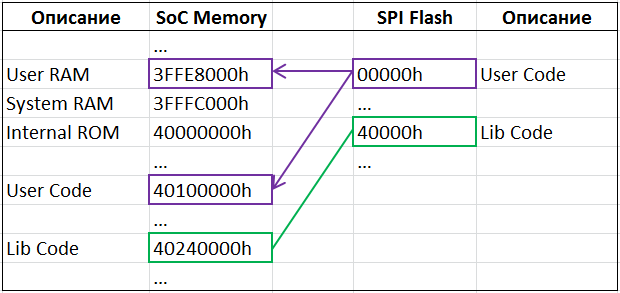
Memory card (address space)
As I said above, the model consists of a flash ROM of 512 KB in size and SoC, which, according to unconfirmed data, has RAM up to 248 KB.
In general, all that concerns memory — the location, properties, and attributes of segments — are community searches. For some reason, this question is bypassed in the original Chinese documentation.
One of the options (there are contradictions with other sources) of the currently known memory card can be viewed here . I will cite only the most interesting addresses:
Inner memory:
| Range | Description |
|---|---|
| 3FFE8000h - 3FFFBFFFh | RAM for user applications. When the module is started, it can be initialized with values from the user firmware. |
| 3FFFC000h - 3FFFFFFFh | system RAM |
| 40000000h - 4000FFFFh | system ROM. From here, the processor starts, the user firmware is loaded, and here are the main system libraries. |
| 40100000h - 4010FFFFh | RAM, contains custom firmware |
| 40240000h - 40271FFFh | The second part of the user firmware. Here are the code of the connected libraries and the SDK. Podampleno to flash at 40000h. |
Different segments of the address space can be RAM, ROM or submapped directly to flash. Podmaplennye areas are cached for speed.
Flash:
| Range | Description |
|---|---|
| 00000h - 3DFFFh | custom firmware download address |
| 40000h - 7BFFFh | SDK library download address (may also be part of user firmware) |
Firmware format
Now, before proceeding to the process of launching the module, consider the format of the firmware. To download a custom firmware, it is usually enough to write 2 data blocks: at the address 00000h and 40000h. The remaining blocks may require flashing to reset the configuration, for example, when uploading a new firmware with an incompatible data format.
A block starting with 40000h contains a simple binary code that is loaded and running unchanged. But the block, starting with 00000h, is a structured data about the segments in it and looks like this:
| Bias | Description |
|---|---|
| 0 | firmware ID, always `0xE9` |
| one | the number of segments in the firmware |
| 2.3 | SPI Flash options |
| 4-7 | firmware launch address (Entry Point) |
| eight... | next are the segment data |
Segment structure:
| Bias | Description |
|---|---|
| 0-3 | segment loading address |
| 4-7 | segment size |
| eight... | next are the segment data |
The final block:
Filled with zeros for alignment to the border of 16 bytes minus 1 byte. After that, the last byte is added, which is the checksum of the data of all segments, calculated by the function xor over all the bytes and the constant `0xEF`.
The firmware format is taken from the description to the esptool utility.
Startup process
Now, armed with this knowledge, consider the process of starting the ESP8266 module from the point of view of initialization and launch of the firmware.
When power is applied or a reset signal is received, the processor starts executing instructions at address 40000080h (system ROM). At address 40001308h, there is a procedure that reads the 00000h flash block and copies the segments stored in it to the specified addresses.
In the diagram, this process is shown in purple. Here you can see that part of the firmware is executable code, and part of it initializes the data in RAM. Green is a block directly podmaplenny in the address space of the processor.
After all initializations, control is transferred to the address specified in the firmware header. Usually this is the address of the user code 40100000h.
3. Tools
Well, now that we’ve dealt with the architecture and start-up procedure of the ESP8266 module, let's move on to learning its program code. What resources and tools do we have for this?
For the design, development and debugging of products based on SoC Xtensa, there is the Xtensa Xplorer package from the processor manufacturer, which includes many utilities, including the TurboXIM - SoC simulator. Theoretically, this utility could be useful, but even the free version requires license keys issued on request. Having written such a request, I did not receive an answer, so I could not use the simulator. Download the full set of tools here , perhaps you will have more luck.
To develop, build firmware, and upload debug information, it will be useful for us to deploy a development environment as described here .
From traditional tools we use IDA Pro and HIEW.
To study the code of the Xtensa processor, you must use IDA Pro version 6.6 and above with a built-in python interpreter to execute scripts. The list of standardly supported Xtensa processors is not included, therefore, each time IDA Pro is launched, before opening the file being investigated, it is necessary to load the “xtensa.py” script, which can be taken here .
Also, to automatically create segments and name functions of the system ROM, we need a script for IDA Pro. The script and dump of system firmware can be downloaded here .
HIEW will be useful for studying the structure of ELF- and pre-built binary firmware files.
In the next part we will look at the process of downloading the firmware for research.
Update. Continued here .
Source: https://habr.com/ru/post/255135/
All Articles