IBM PC do it yourself is easy
After I realized my long-cherished dream and still (albeit with a delay of almost 30 years) built Radio 86RK , for some time it seemed to me that there was quite a decent point on this part of my story.
However, it was found that the disease was not completely cured, and she returned with an even more acute relapse. Probably, both the unexpectedly successful experience of the construction of the 86RK and the fact that during this process I had formed quite a large number of very attractive looking tools, devices and parts, which I really wanted to find a use, affected.
In the end, the breakage became unbearable, and I had to take up the soldering iron again, and also recall some other skills from the past. What came out of this can be seen along with a certain number of pictures and very (I repeat - VERY) with a large number of letters (and not even letters, but pages) further ...
The main question was what to do. On the one hand, the soul was lying to something quite rare, on the other hand I also wanted to try new technologies. Being in heavy thoughts, I periodically looked through a couple of thematic forums dedicated to the old “gland”. At some point, I came across a long stretching topic on how to run an 8086 processor with a minimum of strapping. It was strange that the topic was discussed for more than a year, but it did not move to the practical plane.
')
In my inexperienced glance it seemed that the task was completely trivial, but what if there is something there that I don’t understand at all? As a result, I decided to try to play with this in the hope that this entertainment is exactly what I need for complete happiness.
I didn’t even draw a scheme for myself - everything seems so simple that there were no questions about where to connect. It only remained to decide in what way it is all to collect. I had played enough with MGTF before, I wanted something new. Since everything new is a forgotten old one, I bought the tools and materials for mounting with a wrap and started the process. Which (process), unfortunately, didn’t go anywhere much ... Either my hands were growing from the wrong place, or I understood something wrong, but it wasn’t possible to achieve a stable twist.
However, I did not suffer for long (although perhaps this was the main reason?) - in the process of shifting my treasures from place to place, an unopened bezpayechnaya breadboard with a bunch of very beautiful multicolored wiring was found. The complexity (or rather, the lack thereof) of the project made it possible to easily put everything on this board, which I did quite quickly:
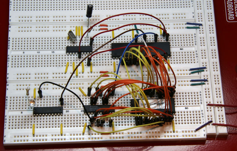
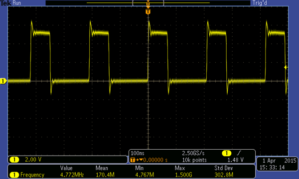
A ten-byte superprogram was written that implements an unparalleled function — the flashing LED. When you first turned on, nothing worked, but it turned out that the problem is only in starting the clock generator. I was too lazy to put the capacitors / resistors specified in the documentation near the quartz, so sometimes to start the generator it was necessary to touch the quartz body with a finger or a screwdriver, after which the LED began to blink regularly.
By the way, I was a little surprised by the blink rate - I already forgot how slow this processor was. At the maximum allowed for the original 8088 clock frequency of 5 MHz, the cycle of 65,536 “empty” operations was performed for about a second ...
Having published the result of my work on the appropriate forum, I was immediately blamed for the connection to 8086, and for me, 8088, which is much simpler and in general!
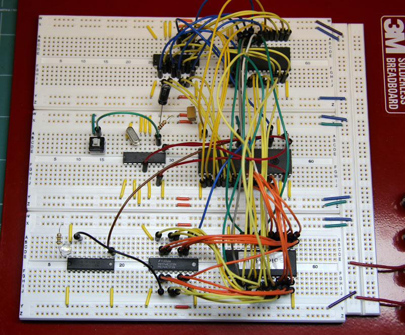
Well, practice is the criterion of truth. I got 8086, spent a little more time (mainly to manually spread the program into two ROM chips, since 8086 is 16-bit, and I had 8-bit ROM) and got another flasher:
Apetite, as we know, comes with eating. So, instead of meeting the satisfaction of what has been achieved, I have a desire to move on. Only here the idea was absolutely firmly established that it is also necessary to try modern technologies. As an example of modern technology, it was decided to use FPGA in combination with the 8088 processor. In one fell swoop it was possible to kill several birds with one stone - the base (processor) is familiar, FPGA technologies are quite modern, and you don’t need to spend time on installation, since all the work can be transferred inside the FPGA.
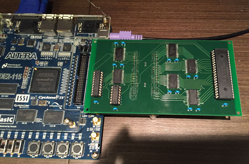
I already had one of the most sophisticated FPGA debugging boards - Terasic DE2-115, on which, besides the rather large Altera Cyclone IV FPGA, the unmeasured number of gadgets, whistles and flashers were also installed:
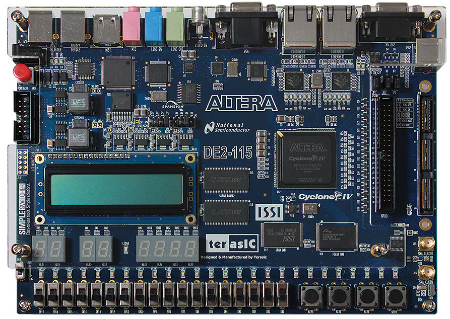
In particular, in addition to regular GPIO in the amount of 36 plus a few more pieces, this board also has an expansion slot, to which you can connect a small fee and get a total of about 100 GPIO, which should be enough for almost any conceivable use (of course, in my modest purposes).
True, there is a nuance - the processor 8088 is 5-volt, but the FPGA has long been abandoned to support TTL 5V, the maximum that is - LVTTL 3.3V
It is good that there is a wide choice of level converters, which was decided to use. First, I stopped on a microcircuit TXB0108 - an 8-bit bidirectional level converter with automatic direction selection. The automatic choice of direction was quite important, since it made it possible not to think about what was happening on the data bus — reading or writing. In addition, the data bus in 8088 is multiplexed with 8 low-order bits of the address bus, which also adds difficulty in determining which direction to transmit signals - from or to the processor.
Since the TXB0108 is rather small, and I didn’t really want to mess around with the wires, I decided to try another new thing for me. The Eagle program for PCB layout was purchased, and my torment began with the development of a new software product in general, and with a very specific Eagle interface in particular.
To do something for the first time in a new area for me personally is very painful for me - you poke like a blind kitten, and your soul is tearing into the open spaces. Preparation of gerber-files for the production of the board (yes, LUT thought about it, and even bought the material, but did not dare) almost caused a nervous breakdown - it immediately seemed like the whole production is standing and laughing, looking at the poor results of my labors ...
It's good that the board was very simple, so it was not even a week (along with the manufacturing time), as I was already holding a freshly soldered piece in my hands:
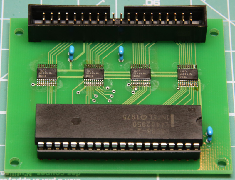
By the way, for soldering level converters, I tried the Ersa “microwave” sting (of course, other manufacturers also have this, and you can do it yourself). I must say, it works quite well, so that the complexity of the soldering was an order of magnitude less than you would expect with such sizes of conclusions.
During the time when the board was made, I was rapidly developing FPGA. In general, I initially bought the debug board to have a little fun with FPGA technologies and, in particular, with VHDL, but this did not go exactly with me. The brain simply refused to think in terms of VHDL, and the maximum that I did was repeat several simple devices in the FPGA, copying their circuits using the circuit design method. The study of the VHDL ended at the level of signal3 <= signal1 and signal2; Further reading of textbooks had a great sleeping effect on me.
Here, too, decided to do everything with the help of circuit design. And in general - what for all these HDLs, when is it so easy to draw a diagram with a mouse, and everything works? At that moment it seemed to me both more correctly and more conveniently. Accordingly, I drew the same flasher in Quartus, but I still had to make an analogue of the 8284 clock generator (I had it in an “iron” form on the breadboard). Fortunately, the documentation found the complete internal structure of this chip, so there were no problems with that. Although one nuance was revealed - in the documentation from Intersil (the manufacturer of outdated microcircuits), the internal structure of 8284 was drawn with an error (the inverse output instead of the direct one, or vice versa, I don’t remember). True, he caught the mistake while considering the scheme, but the fact once again prompted the idea that it was necessary to be guided by the original documents.
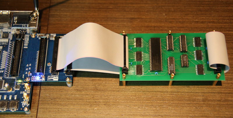
Next, a ROM was generated with the appropriate program, my board with the processor is connected to a flat cable to the debugging board, and the moment of truth came — loading the firmware into the FPGA. Unfortunately, the LED did not blink after that ... After a short trial, it turned out that I applied 0 to one of the processor inputs, whereas there should be 1. This misunderstanding was easily corrected by cutting the track and soldering the jumper. After that, the LED blinked, but it froze in the burning state ...
And here came the real showdown. Unfortunately, I will say right away that I did not understand the reason for the unstable operation of the circuit. I am almost sure that this is due to the fuzzy determination of the directivity of signals through level converters (if only because there is nothing more wrong to work there). The LED could blink for a while, and then generally fail completely, then start working again without any pattern.
All my poking with an oscilloscope did not show anything that could push the real cause, so I had to think about ways to solve the problem in a crucial way - stopping in this place did not allow self-esteem. Since the “self-defined” converters were under a big question, I decided to turn to a more proven solution - 74LVC8T245, level converters with “manual” control of the direction of signal transmission.
In addition, I also decided to expand the task and do everything to the maximum, literally - to start the processor in maximum mode. In this mode, the processor is not the sole owner of the system bus, and can give it to other devices (such as DMA, etc.). It is in this mode that the 8088 works, including in IBM PC compatible computers. To work in the maximum mode, certain signals are necessary, which are usually formed using the 8288 bus controller. Theoretically, these signals could be generated inside the FPGA, but I did not have complete clarity after reading the 8288 documentation quite thoroughly, so it was decided to use “iron” »8288, along with the same 8284 (walk so walk!). The result was a guaranteedly working (as it seemed to me) core, around which it was already possible to build anything.
In the process of thinking about the scheme, once again I came to the conclusion that it was not quite a trivial task to understand the direction of transmission of the address / data bus (precisely because of this, if you remember, I initially tried to use “self-determined” level converters). At first it seems that everything is extremely simple, and there are practically ready signals for this, but on closer examination it turns out that everything is far from being the case (especially if we take into account possible temporary signal scatter and try to fit into them clearly). Therefore, I chose not the most elegant, but the iron-working variant - I allocated a separate level converter for the lower 8 address lines, working in one direction (from the processor) together with a latch (with it, a latch, I got a little excited - it was possible to do FPGA inside) and in parallel to this, another converter was installed on the same lines, whose direction was already controlled by the corresponding signal from 8288 (if we talk only about data, without regard to the address, then everything is unambiguous).
However, due to the fact that the polarity of the direction signal was inverse to what was required for the converter, another 7400 inverter had to be used. But the famous 7400 appeared on the scheme, it is LA3, without which not a single digital device could do at one time .
Once again while the board was in production, I drew a diagram of my supercomputer in Quartus. Unlike the previous version, here I have already decided to add normal address space decoding, to separate memory and I / O, as well as to use RAM. Moreover, instead of a flashing LED, I immediately swung at the whole 7-segment indicator, which was supposed to increase its value in a circle!
Just by the time the drawing scheme was completed, the boards were delivered, the wiring took quite a bit of time, and everything was ready to load the firmware:
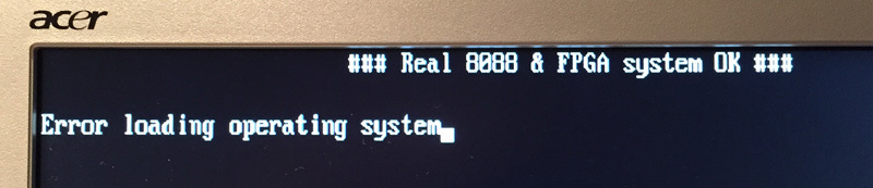
This time, oddly enough, it all worked almost from the "half-poke." The only thing that surprised and alarmed me was the CPU temperature. He really heated up so that after a while it was hardly possible to hold a finger on it. Attempts to look at the oscilloscope, whether there are any conflicts on the tires, led only to the appearance of additional questions, so I turned to one of the professional forums on electronics.
Here you need to make some digression. I have never studied electronics professionally, and I have no education in this field. Moreover, even from an amateur point of view, I had a break in this area for about 20 years (and even before that the experience was rather narrow). Accordingly, I did not know much at all, and understood a lot of what I knew in an idealized form. In particular, the signals in the digital circuit are strictly rectangular, etc. No, I, of course, understood that it was not so, but in practice this understanding could not be applied.
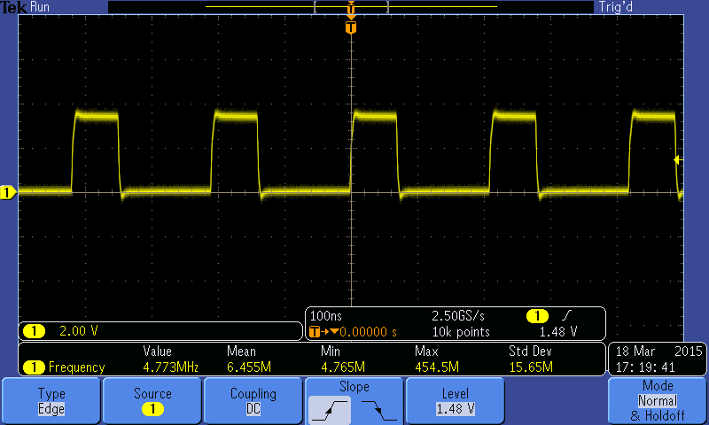
So, on that forum, I opened my eyes to some things that for many will seem to be truisms, but for me it turned out to be a surprise. For example, it seemed to me a strange form of a clock signal coming to the processor with a monstrous amplitude “ringing”:
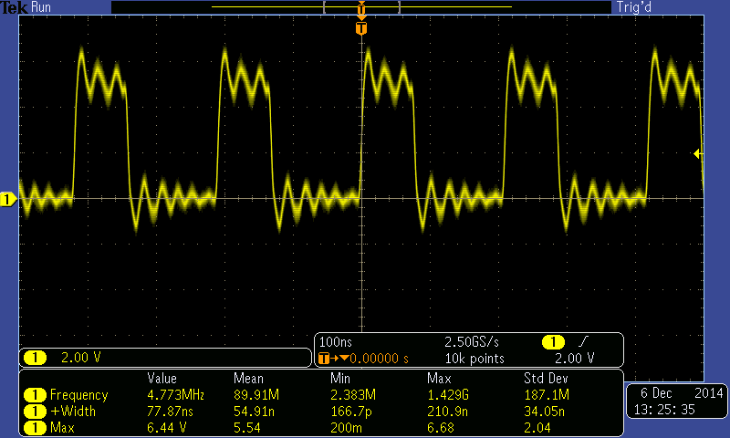
It turned out that this very signal looks completely different, if only the “ground” is taken not where I took it (at the other end of the debug board, as it is more convenient), but directly from the signal receiver (processor):

It seems a trifle, but, in my opinion, it is precisely from such trifles that a true understanding of many processes is formed ...
By the way, about the equipment on which this picture was made. During the fuss with the 86RK, I had a quite good portable oscillograph Fluke, but for some reason I didn’t have a good feeling for it. Why - I don’t know, not that, and that’s all ... So the new project turned out to be a good reason to acquire a new oscilloscope. Having caught fire with the idea, sometimes I make hasty decisions. That is what happened this time. Instead of studying the subject in detail, I got the first device I liked - Tektronix MSO3012. No, I can’t say anything bad about the device, on the contrary - a really convenient interface, a lot of useful functions, a practically full 16-channel analyzer of digital signals, the ability to view signals as a logical bus, connect to a computer both directly and through the network, and .d I just always want more, and one could choose a more modern series - MDO, which, among other things, also offers a built-in arbitrary signal generator. And since the tool is very cool - I already envy those who use such equipment to solve real problems, and not for primitive handicrafts, as in my case ...
Returning to the processor overheating - on the forum I was convinced that for this chip, this temperature is completely normal (just large power consumption). Finally, I calmed down after changing the processor to the one made using more modern technology, and after that it remained completely cold during the whole process.
Having received 8088 with a (potential) heap of peripherals, my hands were very much itching to program something more complicated than managing a 7-segment indicator. True, the question arose of a normal integrated environment for programming in real mode assembler (the only language I knew). And here I was waiting for a big bummer. If for 8080 / Z80, as well as for all modern controllers, there is a mass of both free and commercial IDEs with all imaginable and unimaginable gadgets, then for x86 there was nothing decent at all. There were some abandoned amateur projects, and all. There are several reasons for this, but the fact remains. Ultimately, I stopped at WinAsm (the first thing that somehow worked for me), which I can hardly call a full-fledged IDE (first of all, due to the lack of a debugger), but at least something (like compiling directly from the editor ) he allowed to do. As a debugger at that time I decided to use the old, well-deserved Turbo Debugger, launched in DosBox.
First of all, I wanted to get a normal way to display information for my device, i.e. video adapter Although in a heap of places (including on Habré) you can find articles on the topic “How to write a video adapter on HDL in 5 minutes”, making your module for me was just an unattainable dream. Therefore, I climbed the widely known opencores.org and found the simplest alphanumeric VGA video adapter there, and also on VHDL (most of the projects on opencores are written in Verilog).
Although this module was almost a complete device, nevertheless, to work with my debug board, some refinement was needed (related primarily to the specifics of the digital-analog part of the VGA-interface DE2-115). VHDL, ( ) , - -, , .
- , . FPGA . VGA , . ( ) FPGA. , ( ). , , , ( , ). FPGA – , . , , , – . , – Altera, .
RAM 161M ( , 1024 16- ). ROM, FPGA – flash- , , , .
, 8088 , () . , -.
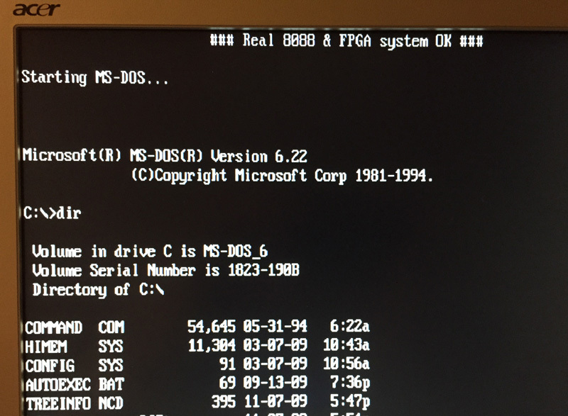
, – «, DOS ?..». , , … , MS-DOS!
, DOS BIOS, «»? , , ( ?) – BIOS' IBM PC. BIOS' DOS, . BIOS , , . , INT 16h, 10h, 13h , .
VHDL PS/2 ( ) . , .
, INT 09h – . . x86 , , . , , mov cmp , . , , - , - . , - -, , … , , - - .
, , , , , , . , …
, INT 09/16 , INT 10h . – .
, . , SD-, , . – , zet.aluzina.org
SD- – SPI .
, SPI , «» , - . , , 8- , , . , , . , , A5, , 0 1 .
SD- , . , , . , — nada-labs.net/2010/using-the-buspirate-with-a-sd-card
, SD ( SDHC - ) . , 0- . INT 13h, INT 19h (boot load) :
0- , ( ), , . – , !
. () . – - ( ). , // , .
, , . , BIOS' , , – . ( – ), . , PC – INT 2F, . , DOS PC, , , , , , . , .
( DOS ), «» ( INT 08h) Shift. :
, – DOS , (- ) ( )!
, . , DOS , Microsoft - . ( , ). – , . DOS, , . , …
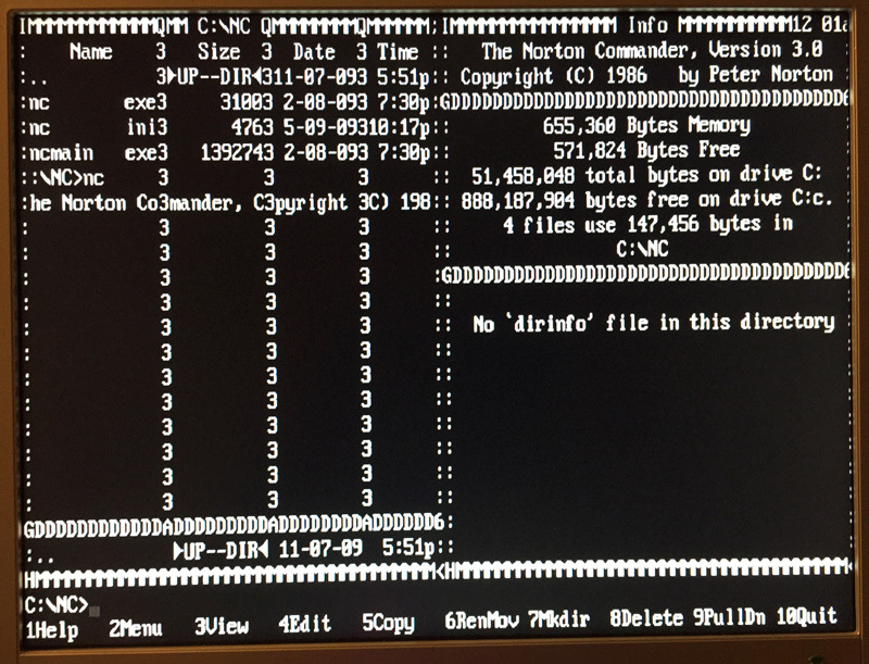
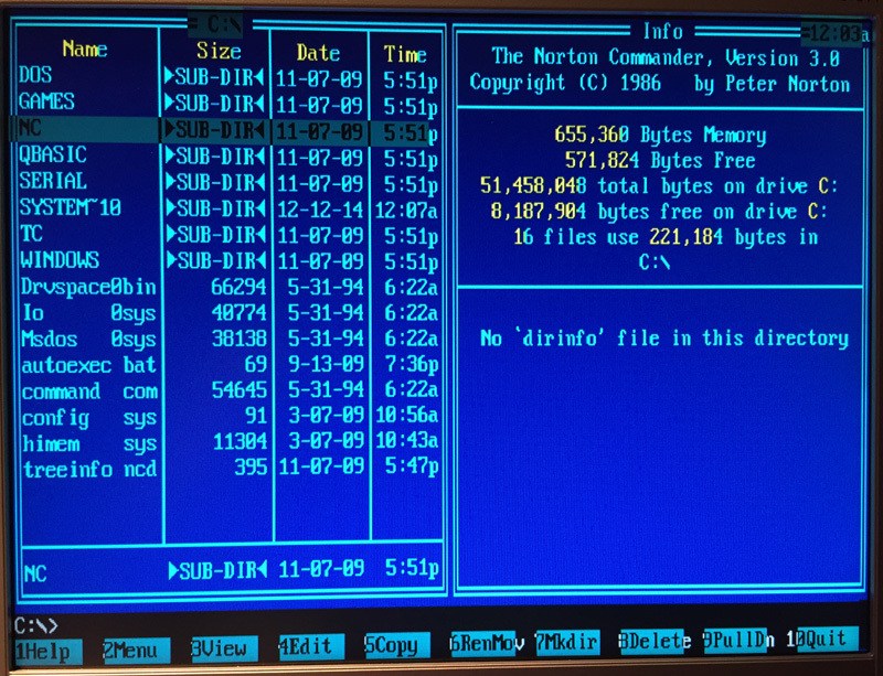
DOS . , , – , , Norton Commander. , , DOS'. NC , , .
, , , NC :
«» :
—
— , ,
— INT 10h.
, ( DOS). , CLS ( ) INT 10h, . , , . , - , . (, ). , …
NC . , , . – ( VHDL ). .
, , VHDL. – - , , , . – 43 ( - ) , 25 . , , VHDL . , , VHDL – -, , - , .
VHDL , - :
, ( ), 80x25 , .
8259. - , ( , , — , , ). IP ( IP Internet Protocol, Intellectual Property), …
() , VHDL. – ( ) , ( ) EOI (End Of Interrupt). , , . , , , - .
, ( ) VHDL – . , ( ) test bench ( , – , ). ModelSim , .
8254 , 18.2 , . , – DOS , NC - . , , .
, – , , . , NC – « ». , , - , , . , , - – , . , , – . , - , .
, , , .. , – , . – , . .
, , , . , . - , , - , , - – , .
. , , – . . . , « , ». – , . - .
, , . , , – 20-30 , . , , . . , . ( ) , ( , ), .
, . , ? FPGA RAM, . , – , . , ! - , , . , , . , – . – , , , .
, . , , – . , , – , , , .
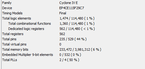
, – , , , , , . , Quartus' , , . , , . , , . , . – , .
– , , , . , …
, DOS , , , , . , - . , , , . , .
. , – , BIOS. , « », - . , , .
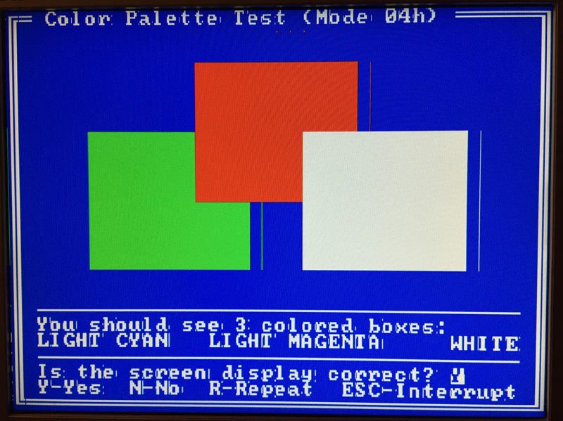
, CGA – EGA , . , - – , , VGA-. , . , , – .
, CGA , VGA 640400, CGA- 320200 , .
– VHDL, , VHDL, . , ( ). , «» FPGA , .
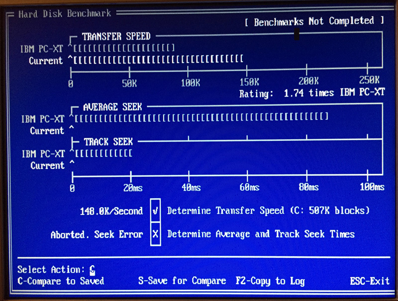
, , , Checkit :
, Checkit – , PC-. Checkit , .
( ) , , , :
– , .
, , «», , - NC QuickBasic. , FPGA , .. , BIOS , . , - ( , ), Turbo Debugger, .
, 8253. ( 2), 0, , .
8253, . . - , opencores . Verilog, , – , VHDL. , VHDL Wishbone – FPGA. Wishbone , Verilog', .
, . , , . , .
. INT 10h . , . , (- , ), « , ». CGA «», BIOS .
, – , . — , . , ( BIOS) , «» .
- , . , 640200 .. , 640200 , . , , :
, …
INT 10h , , .
PC , , . , , . , -, IBM PC. , PC AT, , , -, . , , ( , BIOS). , , (, PC AT PC XT 8051). INT 09/16 , – () -.
VHDL – , , . ( ) VHDL, -. , – . , – .
, . , VHDL ( .., ). – . VHDL ( HDL) , . , , , , , , . , , . – . , , . , , , - .
, -, - VHDL ( Verilog ). , .
, , , . INT 09h, - Checkit' . , 100% .
, . , VHDL, . iMac Retina Windows. , Quartus , . , - . , .
, , . , - , . , , . , VHDL/Verilog. , VHDL vs Verilog – , , /, VHDL. , , . …
VHDL – SPI. , / , . ( INT 13h) 35% PC XT ( Checkit). VHDL , , , .
, DMA (, , ) – DMA , , , . – , . , - , Quartus' SignalTap, , , . , ( ), .
, INT 13h, , . , 5 :
, ( , ) , (, ). , :
— DMA. , DMA ( PC) . DMA
— ( ) / FF. – 00. , ( ) , , ,
— CGA , , , ( ). , , /,
— – Paratrooper. , com/exe . , , , , , 286 . , ( ). , .
, , , , , :
, – . , - Wishbone, VHDL, . , Wishbone Wishbone 8088 – . , . , ( , Wishbone ).
, … , , , ? , :
, , , 2. . 6 , 2. , 2 6 . , 6 2, «»! Those. , . , – . , …
, , , , . , - , 2 . . . , :
, VHDL – . , – . ( ) – , 0 (65536) . 0, , 18.2 . FFFF, .
, () , . , , , - . , , , Verilog.
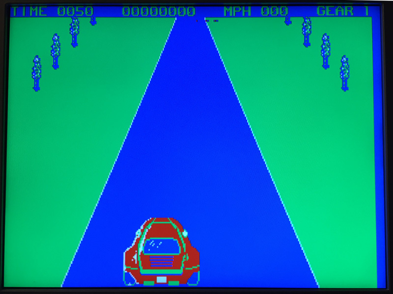
, . , 86 « », «Scientific American», Microsoft – MS Flight Simulator. , , , , ( ).
, 30 , Flight Simulator . , – Flight Simulator, Lotus 1-2-3. , , , .
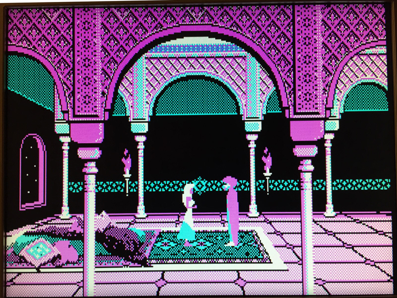
– - , ( , , , ). :

, – - , . , , Microsoft , . , , 320200, , , .
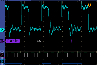
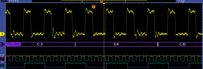
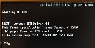
Lotus 1-2-3 , . , , , . , , EMS. , ( , - ), EMS , , . :
. , , Eagle. 4- , , – . , – , FPGA ( , GPIO FPGA – ):
– 8284 (, FPGA, ) - / ( FPGA). , :
, , , . IBM PC, , , .. , «». ( INT 13h) BIOS 3- IBM PC.
- . , — (, ', FPGA ), , , FPGA , ?
, , . , DE2-115, FPGA:
, , , .
( -) – . , , - , , , – , . - - (, ) , VHDL . , – .
Source: https://habr.com/ru/post/254879/
All Articles