FPGA - my first steps
 Recently, I still took my first step to the FPGA and called you after me . My passion for FPGA and the idea that FPGA is the best platform for creating any device has acquired a religious character. My sect PLISovodov preaches a complete rejection of microcontrollers, and a particularly extremist branch preaches a rejection not only of software processors , but also of consecutive calculations!
As always, solving real problems helped comprehend truths. In today's sermon, I would like to tell you about the trials that fall to the lot of the young FPGA. Overcoming trials we comprehend the truth. But there are questions that I have not found the answers. Therefore, I would very much like to see the habrovchane brothers - FPPs with experience, take part in the discussion, extend a helping hand to their younger brethren.
This article is for beginners. In it, I will describe typical problems, questions, delusions, mistakes that may appear at the very beginning of training (because they came to me). However, the context of the article is limited by the fact that the development is carried out on the FPGA from Altera in the environment of Quartus in the Verilog language .
It's hard to live without doing anything, but we are not afraid of difficulties!
One of the reasons why many people are not starting to learn Verilog right now is the lack of a real FPGA. Someone can not order, because it is expensive, but someone because he does not know what to take (the issue of choice is discussed in the previous article ). Someone FPGA still goes by mail.
')
 But in my development I came to the conclusion that I need the presence of a real FPGA at the final stage of development when I need to test the project “in hardware”. The point is that most of the time I spend in debugging my code with the help of simulators.
Therefore, my advice: the absence of FPGAs - this is not a reason to stay inactive. Write and debug modules for FPGA in simulators!
Simulator for Verilog
So, what is to entertain yourself boring long working days (if they are)? Of course we master the FPGA! But how can you drag a whole Altera development environment to work if it weighs 3 monthly Internet limits? You can bring on a flash drive! But if Verilog is the subject of study, then you can limit yourself to a notebook, the Icarus Verilog compiler, and watch the result in GTK Wave.
Try it now
To start working in the Windows environment, simply download the link http://bleyer.org/icarus/ installation file iverilog-20130827_setup.exe (development snapshot) [11.2MB]
Installation does not cause difficulties. Now let's get ahead a bit: create a folder for the project and a couple of files in it with content that is not yet clear:
In the bench.v file, the test module testbench is described, and the test signal source clk (square wave) is created in it. Other modules will be created in separate files, or the logic can be tested first in this module, and then put into a separate module. Then, in the testbench module, instances of these modules will be added, where we will send test signals to their inputs and receive results from them. From the modules we can build a hierarchy, I think this is clear to everyone.
After launching this file, we will see on screen the text specified in $ display (this is debug output), the value of the signals and registers of the circuit will be in the file test.vcd. Click on the file and select the program to view - GTKWave (in my case D: \ iverilog \ gtkwave \ bin \ gtkwave.exe). Just a couple of clicks and we will see our clk.

Installation does not cause difficulties. Now let's get ahead a bit: create a folder for the project and a couple of files in it with content that is not yet clear:
Module file with code for module testing - bench.v
`timescale 1ns / 100 ps module testbench(); reg clk; initial begin $display("start"); $dumpfile("test.vcd"); $dumpvars(0,testbench); clk <= 0; repeat (100) begin #10; clk <= 1; #10; clk <= 0; end $display("finish"); end In the bench.v file, the test module testbench is described, and the test signal source clk (square wave) is created in it. Other modules will be created in separate files, or the logic can be tested first in this module, and then put into a separate module. Then, in the testbench module, instances of these modules will be added, where we will send test signals to their inputs and receive results from them. From the modules we can build a hierarchy, I think this is clear to everyone.
BAT File that compiles and simulates the main module by adding other modules from the current folder - makev.bat
iverilog -o test -I./ -y./ bench.v vvp test pause After launching this file, we will see on screen the text specified in $ display (this is debug output), the value of the signals and registers of the circuit will be in the file test.vcd. Click on the file and select the program to view - GTKWave (in my case D: \ iverilog \ gtkwave \ bin \ gtkwave.exe). Just a couple of clicks and we will see our clk.
 Practically, I create each of my new modules in a notebook and debug IcarusVerilog. The next step after such debugging is checking the modules in Quartus. Although Quartus also has its own simulator, but I use it less often. The reason is the simplicity of updating the code and viewing the result in IcarusVerilog: saved changes in the file, launched BAT, clicked the “refresh” button in GTKWave - that's all! In ModelSim, this requires a little more movement, but it is also not bad, especially on these complex structures.
After the simulation, it is time to launch Quartus. But loading the firmware in the FPGA is still too early. You need to make sure that the divine computer correctly understood the scheme we want to get, setting out our thoughts in the form of Verilog.
The difference between simulation and work in real hardware
At first, I, like a blind kitten, beat my head against the shoals. It would seem that the correct code does not work at all, or it does not work as expected. Either it just worked, but now it has suddenly ceased!
Inquisitive kitten, begins to look for the relationship between their actions and the result ( "dove superstition" ).
Biggest drama
Below is a list of oddities, but first the biggest drama I encountered: not all Verilog constructions can be synthesized in iron . This is due to the fact that Verilog describes not only the hardware logic, which is combined into modules and works in hardware. On the same Verilog, test modules are described that integrate the modules under test, send test signals to their inputs and generally exist only for testing on a computer. The change in signal values over time is given by constructions containing the "#" sign in the Verilog text. This sign means a time delay. In the example above, this is how the CLK signal is generated. And I thought with a sinful deed that in the same way inside this FPGA one can generate, for example, a sequence of bits for sending a message via RS232. After all, the input of the FPGA is a signal from the 50 MHz generator! Maybe she somehow focuses on him. As it turned out, I am not the only one who hoped for a miracle: 1 , 2 , 3 , 4 , 5 . Reality, as always, turns out to be more severe: FPGA is a set of logic and a time delay in it may appear when using a counter, the value of which increases in cycles from the generator to the specified value, or in some other way (but always in hardware).
The list of found oddities
Amazing things, however, reading the books [1,2] sheds light on this devilry. Moreover, grace is gained.
If to designate reg, then not the fact that it will be created
How did I come to the problem? Suppose there is one module, to the input of which I must supply a value (according to the type of the parameter). In the future, this parameter will have to change in time depending on some external events. Therefore, the value must be stored in the register (reg). But the implementation of the reception of external events has not yet been implemented, so I do not change the register, but simply give it the initial value, which does not change later.
// 8 reg [7:0] val; // initial val <= 8'd0240; //wire wire [7:0] out_data; // , bbox // bb_01 // , in_data out_data // val, wire - out_data bbox bb_01(.in_data(val), .out_data(out_data)); It would seem that the catch? In imperative PL, we often set variables as constants and then never change them and everything works. What do we see in the gland?
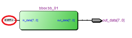
First, we do not see the register. Secondly, the input of the module is 8'hFF instead of our 8'd0240! And this is enough for the scheme to work differently than we planned. The fact that there is no register is normal. In Verilog, you can describe logic in different ways, at the same time, the synthesizer always optimizes the hardware implementation. Even if you write an always block and work with registers in it, but the output value will always be determined by the input, then the use of the register will be superfluous here and the synthesizer will not deliver it. Conversely, if for some values of the input data the output value does not change, then there is no way to do without the register-latch and the synthesizer will create it. (Book 1 pp. 88-89). What follows from this? If we start changing the value of the register, for example, depending on the button presses, the gerister will already be created and everything will work as it should. If it turns out that the buttons do not change anything, then the synthesizer will again throw it out and again everything will break. What to do with the constant? You need to submit it directly to the input of the module:
bbox bb_01(.in_data(8'd0240), .out_data(out_data)); Now at the input of the module we have the correct value:

It remains a mystery why, when reducing the register, its value in initial is not substituted to the input of the module.
The dimension of wire is better to ask yourself.
When developing in the Quartus environment, it is allowed not to define the wire lines in advance. In this case, they will be created automatically, but a warning will be issued about this. The problem is that the wire width will be 1-bit, and if the ports have a bit more than 1 bit, the value will not be transmitted.
bbox bb_01(.in_data(8'd0240), .out_data(int_data)); other_bbox bb_02(.in_data(int_data), .out_data(out_data)); A warning
Warning (10236): Verilog HDL Implicit Net warning at test.v(15): created implicit net for "int_data" Result:
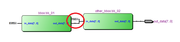
As you can see, one bit is connected, and the remaining 7 bits are not connected (NC). To avoid such a problem - you need to create wire yourself. It is not for nothing that the IcarusVerilog compiler produces not a warning, but an error if the wire is not specified in advance.
wire [7:0] int_data; bbox bb_01(.in_data(8'd0240), .out_data(int_data)); other_bbox bb_02(.in_data(int_data), .out_data(out_data)); 
The computer will not climb on the modules, look, what is the port width. In addition, the bit may be different, and not all the bits are taken to the input of the module or from the output, but some bits.
You cannot use the output of a logic function as a clock signal.
Sometimes in the project it is required to reduce the clock frequency, or to introduce a time delay in N cycles. A novice can apply a counter and an additional scheme for determining whether a counter reaches a certain value (comparison circuit). However, if you directly use the output from the comparison circuit as a clock, problems may arise. This is due to the fact that the logic circuit takes some time to set a stable value at the output. This delay shifts the front of the signal passing through different parts of the logic circuit relative to the clock, as a result we get the race, metastability, asynchronous. It was even possible once to hear a replica of this as a critique of the FPGA: “permanent problems with the FPGAs are signal races”
If you read at least a couple of articles:
Trigger metastability and inter-cycle synchronization
A few words about pipelines in FPGA
then it becomes clear how the FPGA devices are developed: the whole task is divided into hardware blocks, and the data between them move along the conveyors, snapping synchronously in the registers by the clock signal. Thus, knowing the total clock frequency, the synthesizer calculates the maximum frequency of all combinatorial circuits, determines whether their speed is within the tact period and concludes whether the FPGA circuit will or will not work. All this happens at the stage of synthesis. If the schemes fit into the parameters, it is possible to flash the FPGA.
For a complete understanding, it is worthwhile to read the Altera handbook on the subject of “clock domains”, as well as to figure out how to set the calculation parameters of TimeQuest for the project.
Thus, all the necessary methodologies have been created for developers of FPGA-based devices, and if they are followed, then there will be no problems.
And what if I want to go against the system?
The order of development and the behavior of the synthesizer circuits leads us to the conclusion that what is a FPGA at the hardware level. These are synchronous circuits. Therefore, among the goals of the synthesizer - to meet the time intervals. To do this, for example, it simplifies logical expressions, throws out of the synthesis of part of the schemes that are not used by other schemes and are not tied to the physical conclusions of the FPGA. Asynchronous solutions and analog tricks are not welcome, because their work can be unpredictable and depend on anything (voltage, temperature, process technology, batch, FPGA generation), and therefore does not provide a guaranteed, repeatable, portable result. And everyone needs a stable result and common approaches to design!
But what to do if you do not agree with the opinion of the synthesizer that you need to throw out immutable registers, reduce logic circuits? What if you want to make circuits with asynchronous logic? Need some tweaking? Or maybe you yourself want to assemble a circuit on low-level FPGA components? Easy! Thanks to Altera developers for this opportunity and detailed documentation!
How to do it? You can try the graphical editor of schemes. You may have heard that Quartus allows you to draw diagrams? You can choose the standard blocks yourself and connect them. But this is not the solution! Even the drawn scheme will be optimized by the synthesizer, if it will be possible.
As a result, we come to the old truth: if nothing helps, read the instructions . Namely “Altera Handbook” part called “Quartus II Synthesis Options” .
To begin with, by describing the architecture on Verilog in a certain way, you can get a certain result. Here are some code examples for obtaining a synchronous and asynchronous RS trigger:
// RS module rs(clk, r, s, q); input wire clk, r,s; output reg q; always @(posedge clk) begin if (r) begin q <= 0; end else if (s) begin q <= 1; end end endmodule In this case, a synchronous trigger will be obtained.

If you do not take into account the clock signal and switch depending on any changes in r and s, then the result is an element with an asynchronous set of values - a latch.
// RS module ModuleTester(clk, r, s, q); input wire clk, r,s; output reg q; always @(r or s) begin if (r) begin q <= 0; end else if (s) begin q <= 1; end end endmodule 
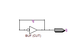
But you can go even further and create a latch from a primitive yourself (primitives are available just like any other Verilog module):
module ModuleTester(clk, r, s, q); input wire clk, r,s; output reg q; DLATCH lt(.q(q), .clrn(~r), .prn(~s)); endmodule As a result, the whole "body kit" at the entrance of the latch, which the synthesizer deemed necessary, will disappear and we will get exactly what we wanted:

A list of existing primitives can be found on the Altera website.
And now a small example about asynchrony and reduction. I thought, for example, to make a generator on the same principle as it was customary to do before, but only on FPGAs:
But to increase the period, I will take 4 elements, but only one of them will be with inversion:
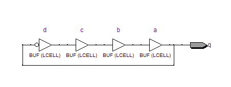
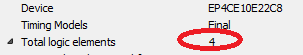
module ModuleTester(q); output wire q; wire a,b,c,d; assign a = b; assign b = c; assign c = d; assign d = ~a; assign q = a; endmodule But it turns out a reduction (1 element, instead of four). What is logical. But we then conceived the delay line.

But if we put the condition to the synthesizer that the lines a, b, c, d are not shortened, then we get what we have in mind. Directives are used to prompt the synthesizer. One way to indicate this is the text in the comment:
module ModuleTester(q); output wire q; wire a,b,c,d /* synthesis keep */; // ^^^--- assign a = b; assign b = c; assign c = d; assign d = ~a; assign q = a; endmodule And here is the result - a chain of four elements:
And that's not all! I leave it to the joy of self-study: work with a case and a directive to implement it as a RAM / ROM or logic circuit; work with built-in memory blocks (RAM / ROM); the choice of the implementation of multiplication - a hardware multiplier or a logic circuit.
findings
To quote the article , I want to say that “FPGAs / FPGAs are not processors,“ programming ”FPGAs (filling the FPGA configuration memory) you create an electronic circuit (hardware), while programming a processor (fixed hardware) you slip a chain of sequential instructions written by the program (software) to him . ”
And, as if I initially did not want to strongly not be attached to a specific piece of iron, but sometimes, in order to use resources more efficiently and economically, I have to work at a low level. Often this can be avoided if you design synchronous circuits correctly. However, completely forget that this iron - does not work.
I also want to say that fanaticism and maximalism diminished with time. At first, I tried to perform all actions and calculations on the FPGA in one clock cycle, because FPGA allows it. However, this is not always required. I have not yet been able to use computational cores of software processors, but using state machines to work on a specific algorithm has become the norm. Calculations are not per 1 clock, time delays of a few clock cycles due to the use of pipelines are the norm.
Books that helped me a lot
1. V.V. Soloviev - Fundamentals of the language of designing digital equipment Verilog. 2014
2. Altera: Quartus II Handbook
3. Altera: Advanced Synthesis Cookbook
4. Altera: Designing with Low-Level Primitives
Articles on the FPGA, Altera and Verilog
FPGA industry news
Microsoft moves to proprietary processors
Intel is going to release Xeon server processors with integrated FPGA
Intel plans to buy Altera
RBC: Intel bought chip maker Altera for $ 16.7 billion
Bing search optimized using neural network on FPGA
Bing search optimized using neural network on FPGA
Intel Xeon processors equip FPGA Altera
Theory
Development of digital devices based on VLSI programmable logic
Hardware features
Trigger metastability and inter-cycle synchronization
FPGA timing analysis or how I mastered Timequest
A few words about pipelines in FPGA
Verilog. RAM wrappers and why it is needed
Designing synchronous circuits. Quick Start with Verilog HDL
Examples
We make a timer or the first project on the FPGA
FPGA clock with Quartus II and some Verilog
How I did a USB device
Color music based on FPGA
FPGA programming. The study of the phenomenon of "contact bounce" and the method of getting rid of it (VHDL!)
Digital IIR filter implementation on Verilog
Verilog. Digital filter on ram
FPGA is easy or do it yourself
VGA adapter on FPGA Altera Cyclone III
The study of the processor and its functional simulation
NES, implementation on FPGA
Video generation by mathematical function on FPGA
Hardware Number Sorter Verilog
Simple SDR receiver on FPGA
Autonomous SDR receiver on FPGA
A look at 10G Ethernet by an FPGA developer
A simple FM radio transmitter based on FPGA
We do tetris under FPGA
Minesweeper on FPGA
Making an IBM PC on FPGA
PS
Thanks to everyone who read to this place. I hope that with this article the principle of operation and use of FPGA will become at least a little closer and more understandable. And as an example of application in a real project,
Source: https://habr.com/ru/post/252261/
All Articles