Time constraints and static time analysis FPGA on the example of Microsemi SmartTime
Even while studying at the university, designing various test gadgets and performing laboratory work on digital circuitry, I got into a situation where the seemingly correct rechecked project several times refuses to work “in hardware”. At that time, at the dawn of learning programmable logic, I somehow very rarely got to get to the last points of Design Flow, in which, probably, the trouble lay. If I accidentally clicked Timing Analyzer with an accidental click, then after a few seconds, a quick glance became boring, and I would return to the bullying over the debug board and write new frenzy on VHDL.
When the time came for more or less adequate and serious projects, there were more problems, respectively, I began to use Google more intensively and search for answers to my questions. Then I increasingly began to come across such terrible phrases as “timing analysis” and “design constraints”, when I read and penetrated a little, I realized that I had missed something very important. At first, I was terribly afraid of these unknown constraints, and without them, the first projects worked successfully, since the frequency there was no more than a couple of tens of MHz. But when it comes to higher frequencies and more complex projects, we can’t do without thorough time analysis and optimization. As I communicated with people, I was surprised to find that not all of our developers are sufficiently familiar with these processes, which is probably due to the very small amount of documentation and explanations in Russian. Therefore, I decided to share what I had accumulated during the work with the FPGA, using tools from the company Microsemi (probably better known as Actel). This post in no case claims 100% completeness and accuracy, just the result of the desire to decompose knowledge on the shelves and, perhaps, help someone to do the same. All comments and suggestions are welcome.
So, as a rule, we are dealing with synchronous circuits. Such schemes consist of the following elements:
')
The connections of these elements constitute the paths of the signals that pass through the device during operation. Actually, I have already identified the key concept - the way . They just determine the performance of the device, in particular, they determine the maximum clock frequency, one of the basic requirements of the project and what developers have been fighting for so long.
The signals begin their journey from the input pins of the microcircuit, pass through sequential and combinational elements and arrive at the output pins. The clock frequency source (CLK) clocks all the triggers of the circuit, which remember the state at its input by the edge of the clock signal (most often on the front). Between the triggers (as well as between I / O ports) is the combinational logic. On the way the signal is prevented by two types of delays:
Usually their ratio is 50/50, that is, the path in the wilds of combinational circuits in half is divided between the delay from the next gate's input to its output and the propagation of the signal along the communication lines. The maximum delay in the circuit corresponds to the critical path , that is, the longest path, which determines the longest period and, accordingly, the maximum frequency of the device. Here it is necessary to consider a few basic concepts.
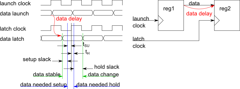
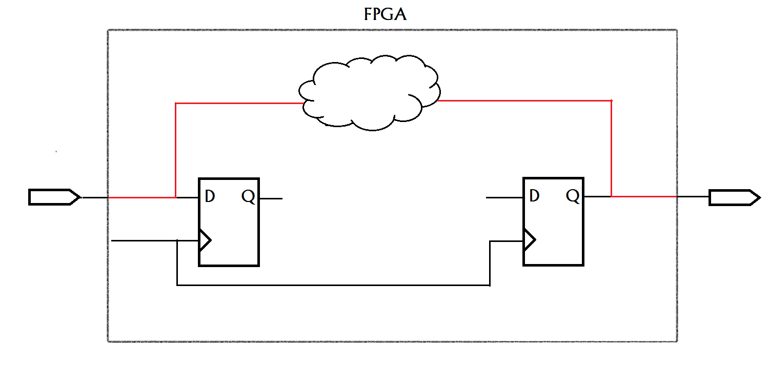
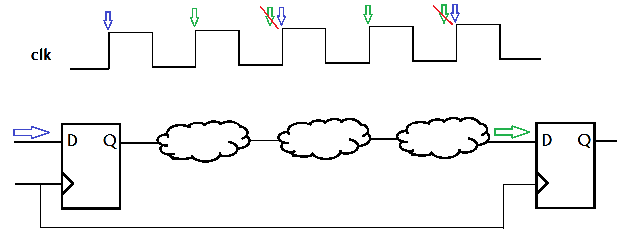
Naturally, when transmitting a signal, two sides of the interaction appear in an obvious way - the source and the receiver. These are the end points of the path. Endpoints can be I / O ports and triggers. Let's stop on triggers. In our case, they are clocked by one clock signal, and the path runs from the output Q of one trigger to the input D of the second. Although the clock signal is one, in this example we give it two names:
Since the data is distributed with a delay caused by the above factors, the signal at the input D of trigger 2 does not appear immediately. This implies the following characteristics:
t su and t h form a kind of corridor, the core of which is the front latch clock. Now the requirements for the signal at the input D of the receiver are simple - it should not change within this corridor. That is, in the ideal case, to be established long before its left border and change the value to a new one some time after the right border. This very time reserve is called Slack. If Slack is a positive number, then everything is in order, and the data will have time to arrive at the receiver input at the required time, if negative - the specified path does not satisfy the time characteristics, that is, the data arrive at the input outside the required time interval, which means the device will not work correctly .
Actually, here the difficulties begin. If you do not have a training scheme with a couple of dozen triggers, but a complicated HDL description that causes headaches when viewing a graphical RTL model, the likelihood of such long paths that dramatically undermine performance increases significantly. In order to control this process and tell the IDE your wishes regarding the project’s time characteristics, the latter contain several handy tools.
Before starting to design a new device, the developer should have as much information as possible about the requirements for this device and its performance. First of all, it is the time characteristics of this system. And when they are known to him, you need to report this to the design tool, and then time limits or time lines come to the rescue . Time constraints are information about the requirements for the project’s time characteristics, set out in a language that is understandable, most often Synopsis Design Constraints, SDC . This is the de facto standard for describing temporal (and not only) constraints for FPGAs, based on Tcl, which, by the way, is in itself commonly used to automate equipment development.
These descriptions are placed in the * .sdc file and attached to the project. Consumers of this file are all kinds of optimizers, who are trying to dilute the crystal so that it meets the requirements of the developer, as well as the time analyzers, which will be discussed further. Sdc files are simple; in fact, this is a list of commands with arguments and their values. When describing, you can (and should) use the Tcl syntax, including special characters, for example, to place a single command on several lines.
So, we list a few basic commands and see what they describe. The first team and definitely must have for absolutely any design:
This command defines the clock signal in the circuit and describes its characteristics:
Name of the string
Period
Duty ratio (default is 2), square brackets indicate an optional argument
Signal source (pin, port)
Knowledge of CAD tools on the clock signal is most important, since without this there can be no analysis and optimization of speech. Then you can further refine the information about the clock signal using the commands set_clock_latency, set_clock_uncertainty, etc., but here we will not consider this, relying on the default values set in the environment. As an example:
This command creates a clock signal with a period of 6 ns, within which the front will be at 0 ns, and the decay at the 3rd.
Another useful command related to the clock signal:
It describes the clock signal that is generated inside the chip, usually in phase-locked loop (PLL) circuits. Actually, the arguments for the most part repeat the settings specified in the PLL — the source of the original signal, the division and multiplication coefficients, the signal inversion, etc. Since PLL is used everywhere, this is also quite an important command, which is common.
Let us proceed to the consideration of the commands that set the limitations and design requirements. The first pair of teams:
Important limitations if the design interacts with external devices (and this is always the case). Sets the delay for the external to the FPGA signal (input or output) with reference to the clock signal. Interacting with other devices, we must take into account their temporal characteristics, for which these two constructions serve. For example, there is our FPGA, any device that exchanges data with us, a clock generator that serves as a common source of clock pulses. In order to effectively conduct a time analysis and tracing, it would be nice to know how the signal will come to us and how we give it to the outside. Usually such information is described in the corresponding datasheets for products, so the task usually comes down to viewing the documentation and rewriting the characteristics into our * .sdc file.

The arguments here are simple - the value of the delay in nanoseconds, the clock signal, optionally indicating whether the delay is maximum or minimum, we can indicate that the binding is declining, and the last is a list of ports to which to apply.
The next pair of commands sets the minimum and maximum delay on the internal path, respectively:
The arguments are, again, simple - the value of the delay in nanoseconds, the starting point and the ending point. Typically, such restrictions apply to purely combinational paths from chip inputs to outputs. This takes into account set_input_delay and set_output_delay and create_clock, if at least one of the end points is a synchronous element. It can also be used for circuits with several clock domains, providing a reliable transition between them.
We will finish the consideration of the timelines by two teams, which serve to determine the paths, the passage of which takes more than one clock cycle and the false paths. Here it is necessary to retreat again to tell what these paths are.
Multicycle path is a path whose endpoints are triggers, which require more than one clock period for the data passing through it to reach the destination point. It is very important to identify such paths, since by default all optimization tools consider the circuit as one-cycle, that is, they try to bring all paths like a trigger-trigger to one clock cycle. For example, some source provides data with a frequency of two times less than the clock frequency. Then there is no point in catching data on every clock cycle, so this path is marked as multicycle and the signals passing through it are given the privilege to stay at 2 clock cycles. If this is not done, our instrument will try in vain to optimize this path, while others may suffer, who just require a pass in one measure.
Flase path - false paths, such paths even though they physically exist, but there is a reason why we want to exclude them from the optimization and time analysis processes, for example, if during the operation of the device the signal never passes through them. A simple example: we have a 4-bit counter, but we only need to count to 9, then the counter is always reset. But it turns out that the increment on larger numbers involves paths with significant delays. They are present, but, in fact, not needed. Such paths are marked as a false path and are thus excluded from optimization and temporal analysis. As in the example with multicycle, if you leave everything as it is, these paths will be optimized with all the ensuing consequences for the rest of the paths.
Commands to tame the above paths:
In both teams, the end points are specified as arguments, and in the case of multicycle, the number of ticks, which are given to the signal to go through the path.
So, we have considered some commands with which you can set time limits and describe the requirements for the time characteristics of the project. Their correct task and attentiveness are the key to success when developing devices on an FPGA, but they might as well create significant difficulties and mistakes that are difficult to track down and fix if you describe unrealistic requirements. Of course, the above is only a drop in the ocean, but it also gives an initial idea and foundation for future study. More information about these commands and their keys can be read for example in [2] . We now turn to the practical part and see how the time analysis looks in Libero SoC, the design tool for the Microsemi / Actel FPGA.
Create requirements and introduce time constraints - this is still half the problem. In this place begins a long and complex process of temporary analysis and the struggle for megahertz. With more or less adequate complexity of the project from the first time to achieve the desired result will not work. Therefore, you will have to revise the requirements, make changes to the constraint file and modify the project itself. Sometimes it is possible to change the FPGA, for example, with the same one, but with greater speedgrade. But in order not to change and immediately understand which chip meets the needs of the project, there are means of static time analysis.
Now the timing analyzer (timing analyzer) is included in every modern CAD equipment development. With the help of this program, the developer can find out whether his aspirations correspond to the capabilities of the newly born (or maybe already a hundred times recompiled) devices before the FPGA firmware and tests on the full-scale sample. In modern CAD systems, they have a convenient graphical interface and are amenable to quick mastering.
Consider the time analyzer on the example of SmartTime enabled in Libero SoC. To do this, we will create in the Libero SoC environment a variation of the classic hello world project for the FPGA with a counter and, using his example, let's look at what the time analyzer allows.
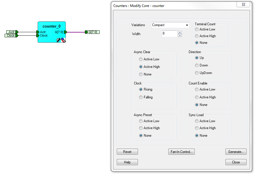
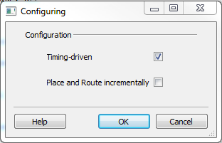
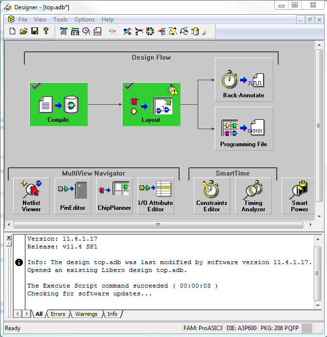
The project selected a simple crystal of the third generation of FPGA Microsemi - ProASIC3 A3P600 with standard speedgrade in the PQ 208 package. To begin with, let's get the project through Design Flow as it is. At the same time in the settings of Place & Route you need to select the optimization criteria for time characteristics (Timing-driven).
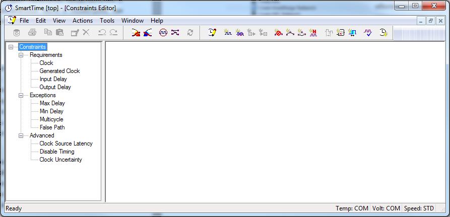
After that, we will have the Designer tool available, which, among other things, contains a shell for managing time constraints and temporal analysis - SmartTime. It is represented by two subsystems - Constraints Editor and Timing Analyzer.
Having opened the Constraints Editor, we can use the user-friendly graphical interface to set the very requirements and restrictions mentioned above and then export the * .sdc file. So do. As indicated above, the first and, of course, the necessary construction is the creation of clock signals with the required characteristics. We have just one, to describe it, follow the menu: Actions -> Constraint -> Clock.
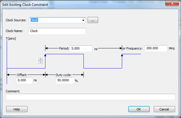
We indicate the pin from which the signal should come and imagine that we need the project to operate at 200 MHz. After clicking OK we will see how the shred appeared in the editor.
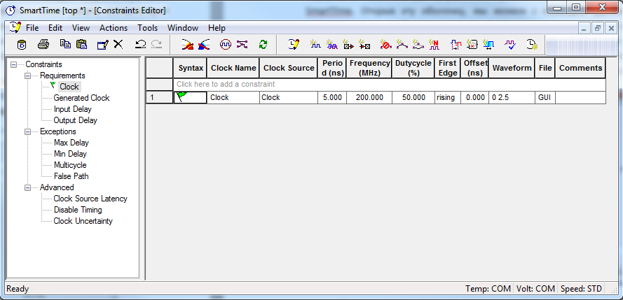
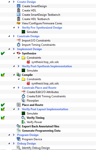
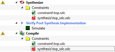
In order for the changes to take effect, click File -> Commit, and from the Designer window, export the file of restrictions by File -> Export -> Constraint Files .... By default, it is placed in the constraint folder in the project root. Let's go back to Design Flow and mark the appeared file top.sdc as used in the Synthesize and Compile sub-items and open it.
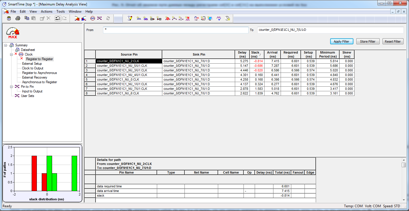
We see a specially formatted file, in which our create_clock is present, and the rest of the fields are empty (the corresponding commands can be in their place if you specify them). Well, we launch Design Flow once again, to the Verify Timing point. Open Designer again and launch the second subsystem - Timing Analyzer. By default, the Maximum Delay Analysis View opens, that is, the time delays calculated based on the worst conditions. Look at the results.
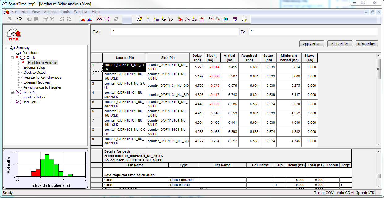
Many have long developed a reflex: red color is bad. There are exceptions, but not in this case. Let's go to the Register-to-Register sub-paragraph, which contains information about the paths between the triggers in the only created clock domain in tabular form. We have some bad results on such paths, a negative Slack has appeared, the time of arrival of the signal at the trigger receiver is more than the calculated maximum allowed. How this threatens is described in the theoretical part at the beginning of the post. The benefit here is not so bad - only five ways showed a negative result. The Slack distribution can be seen in the histogram in the lower left of the window. Let's start to understand. To begin with, let's remember what conditions we asked and see what the analyzer said to that.
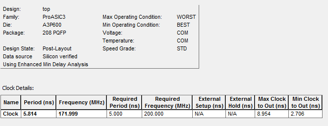
So, we got excited, and our 200 MHz were lowered to 172 MHz f max for this project. Now let's take a closer look at one of the bad ways, for this we will double click on it.
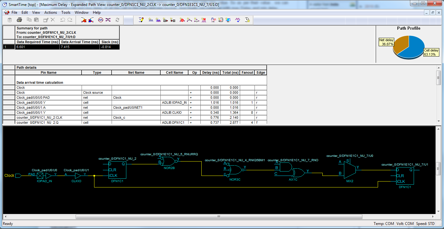
This opens detailed path information. We are shown information about the required time of arrival of data (Data Required Time), time of actual arrival of data (Data Arrival Time) and time margin (Slack). In this case, the path is disclosed in the form of a table with a detailed indication of where and how much the signal is delayed, as well as an image of the connections between the source trigger and the trigger trigger. The tool also shows how it calculates Data Required Time. In the upper right corner you can also see a pie chart showing the ratio of the delays on the valves and the delays on the lines of connections.
Analyzing the results, we come to the conclusion that the delays on the valves of the combination chain on the way from the trigger of the 2nd digit to the trigger of the 7th digit of the counter do not allow the circuit as a whole to operate at the specified frequency. Too long and complex combinational way, data do not have time to arrive at the right time, Slack has a negative value. Such a situation arises at the higher digits for an obvious reason - in order to establish one, the seventh digit needs to make sure that all the others have already been established, respectively there are 8 ways (from all digits, including feedback), and some of them will be unacceptable.
Thus, because of just a few ways, the design does not work at the desired frequency. It's a shame. How to deal with this? The most common way to improve the performance of synchronous circuits is to eliminate a large number of combinational logic between triggers by dividing the process into stages, this is called pipelining . In the general case, with this approach, the input data stream arrives as usual, passes through several stages of the conveyor and appears at the exit after a time dependent on the depth of the conveyor. Depth, that is, the number of steps, is selected based on performance requirements.
Let's return to our project and try to apply this approach to achieve the goal that was set. We divide one 8-bit timer into two 4-bit ones, add a transfer output and a clock enable input. Connect the transfer output of the first timer with the enable input clock of the second timer via a D-flip-flop. We get a two-stage pipeline, the first timer represents the lower digits, the second timer represents the older ones.

Launch the compilation and go to SmartTime. Voila Negative Slacks are gone, there are no errors, the frequency has risen to 227 MHz, which is even much more than we needed.
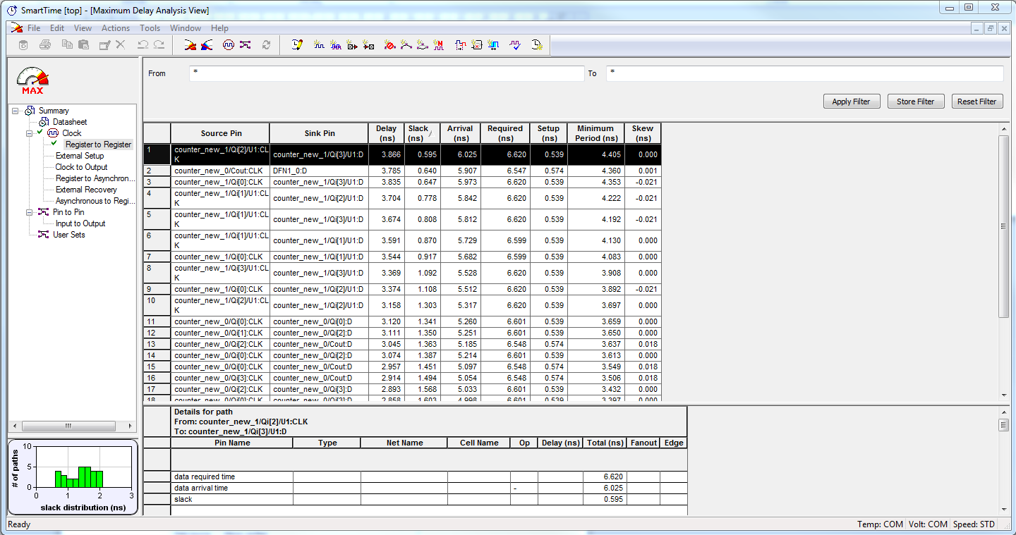
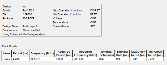
So, using the conveyor technique, we overclocked the frequency of the project with the counter from 172 MHz to 227 MHz, while the functionality was fully preserved, as was the used crystal.
Of course, we looked at a very simple case, and this is all very far from real projects and the actual optimization process, when the red head in the time analyzer window starts to hurt, and it takes days to debug the project. When the example becomes a bit more complicated, a lot of new questions will appear. How to effectively catch multicycle and false paths? How to deal with multiple clock domains? Maybe you can somehow fix the wiring of some elements and fix their temporal characteristics?
But this is a good starting point for beginners to master this difficult task. And, of course, you should try to do the same thing yourself and try to optimize a more complex project.
1. www.microsemi.com , actel.ru - the official website of Microsemi with documentation, the site of the official distributor (information in Russian)
2. www.microsemi.com/index.php?option=com_docman&task=doc_download&gid=131597 - about lines.
3. www.vlsi-expert.com/p/static-timing-analysis.html - about static time analysis.
4. vhdlguru.blogspot.ru/2011/01/what-is-pipelining-explanation-with.html - about pipelining.
5. www.microsemi.com/index.php?option=com_docman&task=doc_download&gid=130940 - SmartTime tutorial.
When the time came for more or less adequate and serious projects, there were more problems, respectively, I began to use Google more intensively and search for answers to my questions. Then I increasingly began to come across such terrible phrases as “timing analysis” and “design constraints”, when I read and penetrated a little, I realized that I had missed something very important. At first, I was terribly afraid of these unknown constraints, and without them, the first projects worked successfully, since the frequency there was no more than a couple of tens of MHz. But when it comes to higher frequencies and more complex projects, we can’t do without thorough time analysis and optimization. As I communicated with people, I was surprised to find that not all of our developers are sufficiently familiar with these processes, which is probably due to the very small amount of documentation and explanations in Russian. Therefore, I decided to share what I had accumulated during the work with the FPGA, using tools from the company Microsemi (probably better known as Actel). This post in no case claims 100% completeness and accuracy, just the result of the desire to decompose knowledge on the shelves and, perhaps, help someone to do the same. All comments and suggestions are welcome.
Synchronous schemes and basic definitions
So, as a rule, we are dealing with synchronous circuits. Such schemes consist of the following elements:
')
- I / O ports;
- consecutive elements (triggers);
- combinational logic (gates).
The connections of these elements constitute the paths of the signals that pass through the device during operation. Actually, I have already identified the key concept - the way . They just determine the performance of the device, in particular, they determine the maximum clock frequency, one of the basic requirements of the project and what developers have been fighting for so long.
The signals begin their journey from the input pins of the microcircuit, pass through sequential and combinational elements and arrive at the output pins. The clock frequency source (CLK) clocks all the triggers of the circuit, which remember the state at its input by the edge of the clock signal (most often on the front). Between the triggers (as well as between I / O ports) is the combinational logic. On the way the signal is prevented by two types of delays:
- cell delay;
- propagation delay;
Usually their ratio is 50/50, that is, the path in the wilds of combinational circuits in half is divided between the delay from the next gate's input to its output and the propagation of the signal along the communication lines. The maximum delay in the circuit corresponds to the critical path , that is, the longest path, which determines the longest period and, accordingly, the maximum frequency of the device. Here it is necessary to consider a few basic concepts.
Naturally, when transmitting a signal, two sides of the interaction appear in an obvious way - the source and the receiver. These are the end points of the path. Endpoints can be I / O ports and triggers. Let's stop on triggers. In our case, they are clocked by one clock signal, and the path runs from the output Q of one trigger to the input D of the second. Although the clock signal is one, in this example we give it two names:
- Launch clock - on the front, new data arrive at output Q of trigger 1;
- Latch clock - on the front trigger 2 remembers what is currently at input D.
Since the data is distributed with a delay caused by the above factors, the signal at the input D of trigger 2 does not appear immediately. This implies the following characteristics:
- Setup time (t su ) - the time for which the signal should be set to the front of clk receiver;
- Hold time (t h ) - the time that the signal should be held after the front clk of the receiver;
- Slack determines the time margin for t su and t h .
t su and t h form a kind of corridor, the core of which is the front latch clock. Now the requirements for the signal at the input D of the receiver are simple - it should not change within this corridor. That is, in the ideal case, to be established long before its left border and change the value to a new one some time after the right border. This very time reserve is called Slack. If Slack is a positive number, then everything is in order, and the data will have time to arrive at the receiver input at the required time, if negative - the specified path does not satisfy the time characteristics, that is, the data arrive at the input outside the required time interval, which means the device will not work correctly .
Actually, here the difficulties begin. If you do not have a training scheme with a couple of dozen triggers, but a complicated HDL description that causes headaches when viewing a graphical RTL model, the likelihood of such long paths that dramatically undermine performance increases significantly. In order to control this process and tell the IDE your wishes regarding the project’s time characteristics, the latter contain several handy tools.
Timing Constraints
Before starting to design a new device, the developer should have as much information as possible about the requirements for this device and its performance. First of all, it is the time characteristics of this system. And when they are known to him, you need to report this to the design tool, and then time limits or time lines come to the rescue . Time constraints are information about the requirements for the project’s time characteristics, set out in a language that is understandable, most often Synopsis Design Constraints, SDC . This is the de facto standard for describing temporal (and not only) constraints for FPGAs, based on Tcl, which, by the way, is in itself commonly used to automate equipment development.
These descriptions are placed in the * .sdc file and attached to the project. Consumers of this file are all kinds of optimizers, who are trying to dilute the crystal so that it meets the requirements of the developer, as well as the time analyzers, which will be discussed further. Sdc files are simple; in fact, this is a list of commands with arguments and their values. When describing, you can (and should) use the Tcl syntax, including special characters, for example, to place a single command on several lines.
So, we list a few basic commands and see what they describe. The first team and definitely must have for absolutely any design:
create_clock -name name -period period_value [-waveform edge_list] source This command defines the clock signal in the circuit and describes its characteristics:
Name of the string
-name name Period
-period period_value Duty ratio (default is 2), square brackets indicate an optional argument
[-waveform edge_list] Signal source (pin, port)
source Knowledge of CAD tools on the clock signal is most important, since without this there can be no analysis and optimization of speech. Then you can further refine the information about the clock signal using the commands set_clock_latency, set_clock_uncertainty, etc., but here we will not consider this, relying on the default values set in the environment. As an example:
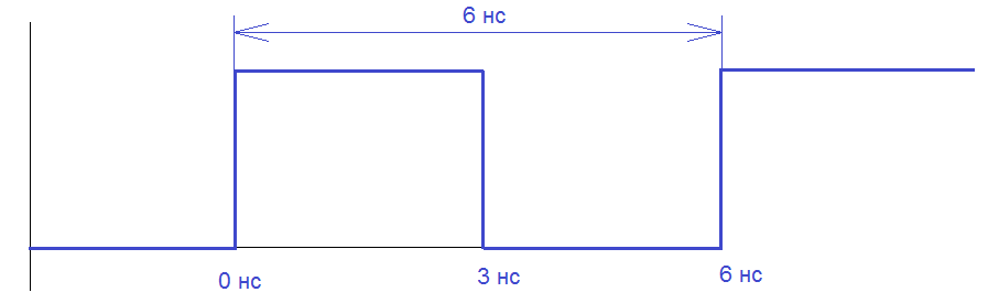
create_clock -name {my_clock} –period 6 –waveform {0 3} {CLK} This command creates a clock signal with a period of 6 ns, within which the front will be at 0 ns, and the decay at the 3rd.
Another useful command related to the clock signal:
create_generated_clock -name {name -source reference_pin [-divide_by divide_factor] [-multiply_by multiply_factor] [-invert] source It describes the clock signal that is generated inside the chip, usually in phase-locked loop (PLL) circuits. Actually, the arguments for the most part repeat the settings specified in the PLL — the source of the original signal, the division and multiplication coefficients, the signal inversion, etc. Since PLL is used everywhere, this is also quite an important command, which is common.
Let us proceed to the consideration of the commands that set the limitations and design requirements. The first pair of teams:
set_input_delay delay_value -clock clock_ref [–max] [–min] [–clock_fall] input_list set_output_delay delay_value -clock clock_ref [–max] [–min] [–clock_fall] output_list Important limitations if the design interacts with external devices (and this is always the case). Sets the delay for the external to the FPGA signal (input or output) with reference to the clock signal. Interacting with other devices, we must take into account their temporal characteristics, for which these two constructions serve. For example, there is our FPGA, any device that exchanges data with us, a clock generator that serves as a common source of clock pulses. In order to effectively conduct a time analysis and tracing, it would be nice to know how the signal will come to us and how we give it to the outside. Usually such information is described in the corresponding datasheets for products, so the task usually comes down to viewing the documentation and rewriting the characteristics into our * .sdc file.
The arguments here are simple - the value of the delay in nanoseconds, the clock signal, optionally indicating whether the delay is maximum or minimum, we can indicate that the binding is declining, and the last is a list of ports to which to apply.
The next pair of commands sets the minimum and maximum delay on the internal path, respectively:
set_min_delay delay_value [-from from_list] [-to to_list] set_max_delay delay_value [-from from_list] [-to to_list] The arguments are, again, simple - the value of the delay in nanoseconds, the starting point and the ending point. Typically, such restrictions apply to purely combinational paths from chip inputs to outputs. This takes into account set_input_delay and set_output_delay and create_clock, if at least one of the end points is a synchronous element. It can also be used for circuits with several clock domains, providing a reliable transition between them.
We will finish the consideration of the timelines by two teams, which serve to determine the paths, the passage of which takes more than one clock cycle and the false paths. Here it is necessary to retreat again to tell what these paths are.
Multicycle path is a path whose endpoints are triggers, which require more than one clock period for the data passing through it to reach the destination point. It is very important to identify such paths, since by default all optimization tools consider the circuit as one-cycle, that is, they try to bring all paths like a trigger-trigger to one clock cycle. For example, some source provides data with a frequency of two times less than the clock frequency. Then there is no point in catching data on every clock cycle, so this path is marked as multicycle and the signals passing through it are given the privilege to stay at 2 clock cycles. If this is not done, our instrument will try in vain to optimize this path, while others may suffer, who just require a pass in one measure.
Flase path - false paths, such paths even though they physically exist, but there is a reason why we want to exclude them from the optimization and time analysis processes, for example, if during the operation of the device the signal never passes through them. A simple example: we have a 4-bit counter, but we only need to count to 9, then the counter is always reset. But it turns out that the increment on larger numbers involves paths with significant delays. They are present, but, in fact, not needed. Such paths are marked as a false path and are thus excluded from optimization and temporal analysis. As in the example with multicycle, if you leave everything as it is, these paths will be optimized with all the ensuing consequences for the rest of the paths.
Commands to tame the above paths:
set_multicycle_path ncycles [-from from_list] [–through through_list] [-to to_list] set_false_path [-from from_list] [-through through_list] [-to to_list] In both teams, the end points are specified as arguments, and in the case of multicycle, the number of ticks, which are given to the signal to go through the path.
So, we have considered some commands with which you can set time limits and describe the requirements for the time characteristics of the project. Their correct task and attentiveness are the key to success when developing devices on an FPGA, but they might as well create significant difficulties and mistakes that are difficult to track down and fix if you describe unrealistic requirements. Of course, the above is only a drop in the ocean, but it also gives an initial idea and foundation for future study. More information about these commands and their keys can be read for example in [2] . We now turn to the practical part and see how the time analysis looks in Libero SoC, the design tool for the Microsemi / Actel FPGA.
Time Analysis in Libero SoC SmartTime
Create requirements and introduce time constraints - this is still half the problem. In this place begins a long and complex process of temporary analysis and the struggle for megahertz. With more or less adequate complexity of the project from the first time to achieve the desired result will not work. Therefore, you will have to revise the requirements, make changes to the constraint file and modify the project itself. Sometimes it is possible to change the FPGA, for example, with the same one, but with greater speedgrade. But in order not to change and immediately understand which chip meets the needs of the project, there are means of static time analysis.
Now the timing analyzer (timing analyzer) is included in every modern CAD equipment development. With the help of this program, the developer can find out whether his aspirations correspond to the capabilities of the newly born (or maybe already a hundred times recompiled) devices before the FPGA firmware and tests on the full-scale sample. In modern CAD systems, they have a convenient graphical interface and are amenable to quick mastering.
Consider the time analyzer on the example of SmartTime enabled in Libero SoC. To do this, we will create in the Libero SoC environment a variation of the classic hello world project for the FPGA with a counter and, using his example, let's look at what the time analyzer allows.
The project selected a simple crystal of the third generation of FPGA Microsemi - ProASIC3 A3P600 with standard speedgrade in the PQ 208 package. To begin with, let's get the project through Design Flow as it is. At the same time in the settings of Place & Route you need to select the optimization criteria for time characteristics (Timing-driven).
After that, we will have the Designer tool available, which, among other things, contains a shell for managing time constraints and temporal analysis - SmartTime. It is represented by two subsystems - Constraints Editor and Timing Analyzer.
Having opened the Constraints Editor, we can use the user-friendly graphical interface to set the very requirements and restrictions mentioned above and then export the * .sdc file. So do. As indicated above, the first and, of course, the necessary construction is the creation of clock signals with the required characteristics. We have just one, to describe it, follow the menu: Actions -> Constraint -> Clock.
We indicate the pin from which the signal should come and imagine that we need the project to operate at 200 MHz. After clicking OK we will see how the shred appeared in the editor.
In order for the changes to take effect, click File -> Commit, and from the Designer window, export the file of restrictions by File -> Export -> Constraint Files .... By default, it is placed in the constraint folder in the project root. Let's go back to Design Flow and mark the appeared file top.sdc as used in the Synthesize and Compile sub-items and open it.
################################################################################ # SDC WRITER VERSION "3.1"; # DESIGN "top"; # Timing constraints scenario: "Primary"; # DATE "Mon Feb 16 10:48:26 2015"; # VENDOR "Actel"; # PROGRAM "Microsemi Libero Software Release v11.4 SP1"; # VERSION "11.4.1.17" Copyright (C) 1989-2014 Actel Corp. ################################################################################ set sdc_version 1.7 ######## Clock Constraints ######## create_clock -name { Clock } -period 5.000 -waveform { 0.000 2.500 } { Clock } ######## Generated Clock Constraints ######## ######## Clock Source Latency Constraints ######### ######## Input Delay Constraints ######## ######## Output Delay Constraints ######## ######## Delay Constraints ######## ######## Delay Constraints ######## ######## Multicycle Constraints ######## ######## False Path Constraints ######## ######## Output load Constraints ######## ######## Disable Timing Constraints ######### ######## Clock Uncertainty Constraints ######### We see a specially formatted file, in which our create_clock is present, and the rest of the fields are empty (the corresponding commands can be in their place if you specify them). Well, we launch Design Flow once again, to the Verify Timing point. Open Designer again and launch the second subsystem - Timing Analyzer. By default, the Maximum Delay Analysis View opens, that is, the time delays calculated based on the worst conditions. Look at the results.
Many have long developed a reflex: red color is bad. There are exceptions, but not in this case. Let's go to the Register-to-Register sub-paragraph, which contains information about the paths between the triggers in the only created clock domain in tabular form. We have some bad results on such paths, a negative Slack has appeared, the time of arrival of the signal at the trigger receiver is more than the calculated maximum allowed. How this threatens is described in the theoretical part at the beginning of the post. The benefit here is not so bad - only five ways showed a negative result. The Slack distribution can be seen in the histogram in the lower left of the window. Let's start to understand. To begin with, let's remember what conditions we asked and see what the analyzer said to that.
So, we got excited, and our 200 MHz were lowered to 172 MHz f max for this project. Now let's take a closer look at one of the bad ways, for this we will double click on it.
This opens detailed path information. We are shown information about the required time of arrival of data (Data Required Time), time of actual arrival of data (Data Arrival Time) and time margin (Slack). In this case, the path is disclosed in the form of a table with a detailed indication of where and how much the signal is delayed, as well as an image of the connections between the source trigger and the trigger trigger. The tool also shows how it calculates Data Required Time. In the upper right corner you can also see a pie chart showing the ratio of the delays on the valves and the delays on the lines of connections.
Analyzing the results, we come to the conclusion that the delays on the valves of the combination chain on the way from the trigger of the 2nd digit to the trigger of the 7th digit of the counter do not allow the circuit as a whole to operate at the specified frequency. Too long and complex combinational way, data do not have time to arrive at the right time, Slack has a negative value. Such a situation arises at the higher digits for an obvious reason - in order to establish one, the seventh digit needs to make sure that all the others have already been established, respectively there are 8 ways (from all digits, including feedback), and some of them will be unacceptable.
Thus, because of just a few ways, the design does not work at the desired frequency. It's a shame. How to deal with this? The most common way to improve the performance of synchronous circuits is to eliminate a large number of combinational logic between triggers by dividing the process into stages, this is called pipelining . In the general case, with this approach, the input data stream arrives as usual, passes through several stages of the conveyor and appears at the exit after a time dependent on the depth of the conveyor. Depth, that is, the number of steps, is selected based on performance requirements.
Let's return to our project and try to apply this approach to achieve the goal that was set. We divide one 8-bit timer into two 4-bit ones, add a transfer output and a clock enable input. Connect the transfer output of the first timer with the enable input clock of the second timer via a D-flip-flop. We get a two-stage pipeline, the first timer represents the lower digits, the second timer represents the older ones.
Launch the compilation and go to SmartTime. Voila Negative Slacks are gone, there are no errors, the frequency has risen to 227 MHz, which is even much more than we needed.
So, using the conveyor technique, we overclocked the frequency of the project with the counter from 172 MHz to 227 MHz, while the functionality was fully preserved, as was the used crystal.
Conclusion
Of course, we looked at a very simple case, and this is all very far from real projects and the actual optimization process, when the red head in the time analyzer window starts to hurt, and it takes days to debug the project. When the example becomes a bit more complicated, a lot of new questions will appear. How to effectively catch multicycle and false paths? How to deal with multiple clock domains? Maybe you can somehow fix the wiring of some elements and fix their temporal characteristics?
But this is a good starting point for beginners to master this difficult task. And, of course, you should try to do the same thing yourself and try to optimize a more complex project.
References:
1. www.microsemi.com , actel.ru - the official website of Microsemi with documentation, the site of the official distributor (information in Russian)
2. www.microsemi.com/index.php?option=com_docman&task=doc_download&gid=131597 - about lines.
3. www.vlsi-expert.com/p/static-timing-analysis.html - about static time analysis.
4. vhdlguru.blogspot.ru/2011/01/what-is-pipelining-explanation-with.html - about pipelining.
5. www.microsemi.com/index.php?option=com_docman&task=doc_download&gid=130940 - SmartTime tutorial.
Source: https://habr.com/ru/post/252247/
All Articles