SoC: we raise simple DMA on FPGA
Good afternoon! In the last article I described how to “raise” SoC from Altrera from scratch .
We stopped at measuring the bandwidth between the CPU and the FPGA when copying is done by the processor.
This time we will go a little further and implement a primitive DMA in FPGA.
Who cares - welcome under cat.
Iron used
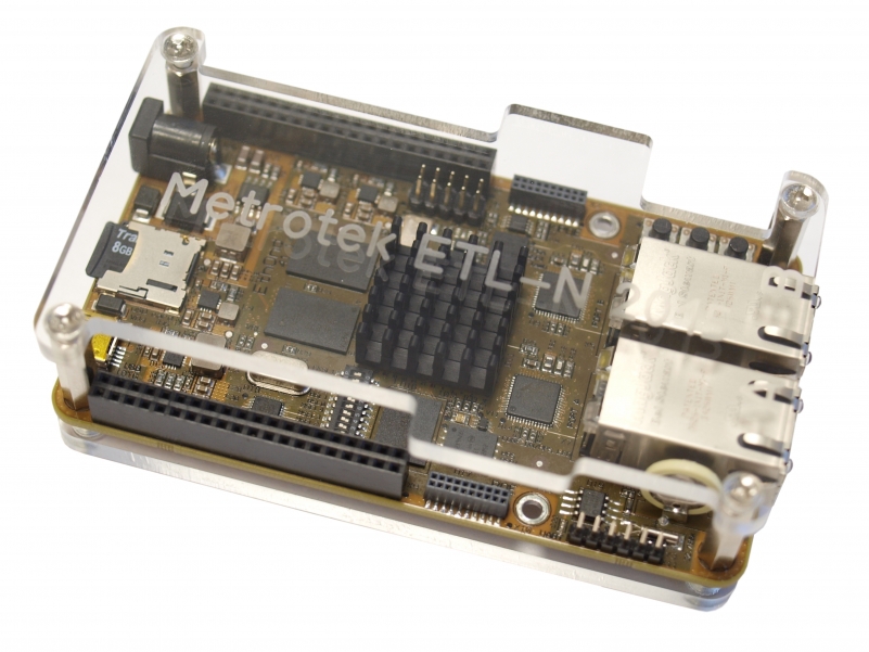
Last time we used the SoCrates fee from EBV .
This time I will use our own development board - it is this one that is represented in the photo.
')
The main difference is in our motherboard 2 Gigabit Ethernet interfaces and they are not installed on the CPU, but on the FPGA.
This allows very flexible traffic handling. Plus, the connectors displayed a large number of pins.
But these differences will become fundamental for us only in the following articles.
In one we will implement NIC in FPGA - for this, of course, we will use gigabit interfaces. In the other we will write support for the framebuffer for the ILI9341 display, again, in the FPGA - this will require an expansion card.
And to perform the actions described below, any board with SoC Cyclone V
Source
In the course of the article I will give only important pieces of code with explanations.
The whole source code can be viewed on github
Detailing
Details of building the kernel, getting the bootloader and other actions described in the last article , I will not give.
A note about the kernel - it is better to use a more recent kernel version 3.18 from here:
git clone git://git.rocketboards.org/linux-socfpga.git git checkout remotes/origin/socfpga-3.18 We think about the implementation
Choosing a DMA Controller
So, our goal is to transfer data from the FPGA to the processor and / or back with the maximum bandwidth and minimum CPU load.
The copying option by the processor immediately disappears, you need to use DMA. But who can fulfill the role of a DMA controller?
For our SoC, there are two options - either FPGA or DMA-330 controller built into the HPS .
Judging by the discussions on the network, the DMA-330 is not very productive, and the corresponding driver may not even be fully functional.
Maybe someday we will try to revive the DMA-330, but now our choice is FPGA
Interface selection
To perform the functions of a DMA controller, the FPGA must be a master. This is possible to implement on one of two interfaces:
- FPGA-to-HPS ( fpga2hps )
- FPGA-to-HPS SDRAM ( fpga2sdram )
Block diagram of the HPS components and the interfaces between them:
HPS architecture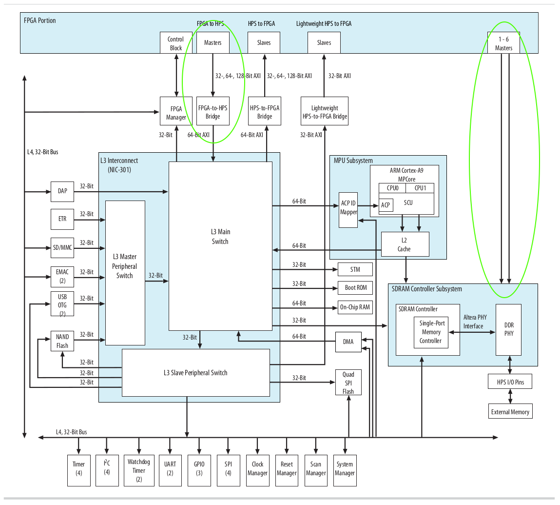
Let's see what the advantages and disadvantages of each option.
fpga2hps allows wizards in FPGA to access almost all of the slaves in the system. That is, not only as a memory, but also to a diverse periphery.
fpga2sdram allows FPGA to work with DDR-memory, "owned" HPS. In this case, access is limited to RAM only.
fpga2sdram allows you to get more bandwidth.
When using fpga2hps exchange occurs through a single interface. If the FPGA requires multiple masters, then arbitration is required. So you need to either write your own modules, or use those generated with Qsys, and they are quite resource-intensive.
On the other hand, in fpga2sdram you can create up to 6 independent ports, and all issues with arbitration will be decided by the DDR controller.
Attention: the number 6 is not quite “fair” - 6 command ports are available, 4 ports for writing and 4 ports for reading.
In this case, one 128-bit interface requires the use of the 1st command port, 2 ports for writing and 2 ports for reading.
Both fpga2hps and fpga2sdram must be initialized to write to the appropriate registers before use. Unfortunately, for fpga2sdram this needs to be done after the FPGA firmware, but at the moment when no transactions on the interface occur. In fact, when using Linux , this means that you need to flash FPGAs in the U-boot. Details can be read here .
When working with fpga2hps, the master in FPGA must use the byte address; when working with fpga2sdram , the address of the word.
More information can be found in the Cyclone V Device Handbook Volume 3: Hard Processor System Technical Reference Manual .
Chapters 8 HPS-FPGA Bridges and 11 SDRAM Controller Subsystem .
For our task there is no fundamental difference what to use. Let's select fpga2sdram in the hope of getting more bandwidth.
Choice of implementation of the DMA controller
We have decided that we will implement the DMA controller in the FPGA and with what interface it will work.
But how are we going to do the controller itself? You can use one of the open "crusts", for example , this one , which is also available through Qsys.
This is a good DMA controller, which has many useful features. We will return to it when we implement our NIC .
But now for our task such a controller is an unnecessary functionality and excessive complexity.
For the learning task, it is much better to sketch a couple of counters in the FPGA, in order to realize that the essence of the DMA controller is very simple.
Upper level
From the software side, everything is also quite simple - we need a driver that will allocate memory, get the bus address of this memory, configure and run the DMA controller in the FPGA, wait for the transaction to complete, and receive data.
And we will write it. But we will start not with the driver, but with a slightly strange program in the userspace , which will perform the same functions.
This will allow us to work with DMA controllers in FPGAs without having to write something at the kernel level.
For “production”, such solutions are usually not used, but for debugging it is sometimes convenient.
For simplicity, the firmware in the FPGA will transfer data in the direction of FPGA -> CPU.
Data transmission in the opposite direction is almost completely similar, with the exception of one nuance, which will be discussed below.
With the direction of CPU -> FPGA, we will work when implementing a framebuffer for LCD .
So the plan:
- FPGA Firmware
- Program in userspace
- Kernel driver
FPGA firmware implementation
Let's start with our beloved Qsys. We need three IP peels:
- Processors and Peripherals -> Hard Processor Systems -> Arria V / Cyclone V Hard Processor System
- Basic Functions -> Bridges and Adapters -> Memory Mapped -> Avalon-MM Pipeline Bridge
- Basic Functions -> Bridges and Adapters -> Clock -> Clock Bridge
For HPS, we leave it almost the same as in the previous article.
On the FPGA Interfaces tab, you need to add the FPGA-to-HPS SDRAM interface.
Choose type Avalon-MM Bidirectional , width - 128 bits.
You also need to check the box next to Enable FPGA-to-HPS Interrupts .
This will allow our DMA controller to “inform” the CPU of the completion of a transaction through an interrupt.
Also, the width of the HPS-to-FPGA interface must be set to 64 bits. This is the interface through which the CPU will configure the DMA controller.
Its width can be any, we set 64 bits simply because I had chosen such a width, and the source code, described below, is set to this value.
This is what should happen:
FPGA Interfaces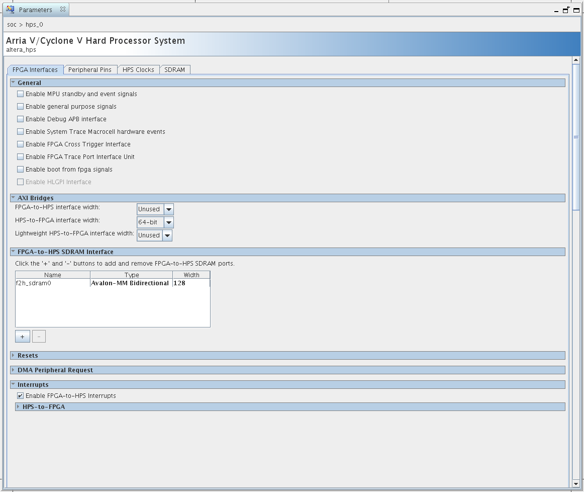
Go to Avalon-MM Bridge .
This peel will act as a converter. We need to export the HPS-to-FPGA from the auto-generated Qsys module to the outside.
But if we just do this, we get the AXI interface, which is much more complicated than Avalon-MM . And we don’t want to work with them at all. After adding this module, Qsys automatically converts AXI to Avalon. It will take some resources, but it will be much more convenient to work.
You need to configure the module as follows:
Avalon-MM Bridge
Go to the last module. It is needed so that we can export the shred from the HPS to the outside and synchronize the DMA controller over this shred. Its setup is primitive - you just need to specify the number of clocks equal to 1.
After that you need to connect all our modules (note the names in the Export column):
Qsys Connections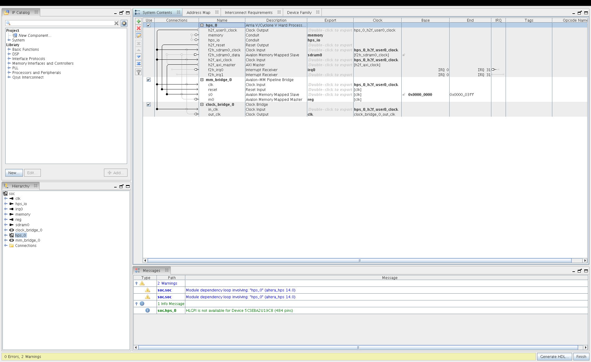
It remains to save and generate files.
The time has come to implement our primitive DMA controller. How are we going to customize it?
To configure, we will use the so-called Control and Status Registers (Control and Status Register, CSR )
These are fixed-size blocks that are read / write (control) or read-only (status) CPUs available.
Access to these registers will be via HPS-to-FPGA .
Since the interface is 64 bits wide, you can either make registers of the same width or add a converter.
Making registers 64-bit is very expensive. Indeed, very often in the whole register only a few bits are used.
It is better to make the registers 16-bit, and if it becomes necessary to have a word of high resolution use 2 or 4 adjacent registers.
Theoretically, it was possible to use a converter generated by Qsys, specifying a 16-bit width for the Avalon-MM Bridge peel, but in practice this could not be done - Qsys generated a non-working module. No problem, we will use our own :)
The avalon_width_adapter.sv module is used as a converter, and the registers themselves are implemented in the regfile_with_be.v module .
The logic of the register module is extremely simple - depending on the address, we put the contents of the necessary register on the bus read data. If the recording signal also came, then we save the input data in the register. The address specifies the register number, not the byte number. The method of dividing into control and status registers is set by the parameter during assembly — either by the high-order bit of the address (the address space in this case is divided equally between the control and status registers) or by the number of registers specified by the parameters.
Go directly to the DMA-controller. For simplicity, it is located in the top module .
All that our DMA controller will consist of is three counters and a pair of signals.
Let me remind you that the data our controller issues on the interface Avalon-MM . A detailed description can be found here , but in general it is a fairly simple interface.
In order to record the data, you need to set the following signals:
- sdram0_address is an address (I remind you that for fpga2sdram this should be the address of a word).
- sdram0_writedata - data to write.
- sdram0_byteenable - a signal indicating which bytes from the data to write. For simplicity, we set it equal to 16'hFFFF .
- sdram0_burstcount - signal to control the burst. Again, for simplicity, we set it equal to 1.
- sdram0_write - this signal must be set to 1 to execute a write transaction
The only caveat to remember is the presence of the sdram0_waitrequest signal. If it is equal to 1, this means that the slave cannot process the transaction at the moment and the master must leave all its signals unchanged. Exactly how often the sdram0_waitrequest signal will be set to 1 and will ultimately determine the throughput of our DMA.
So, we describe the used counters. The first is the address counter, addr_cnt . When a DMA transaction starts, it is set to the address specified by the CPU. After each successful transaction (when sdram0_waitrequest is not equal to 1), this counter is incremented by 1.
The second is a data_cnt counter for data emulation. You can write to the data whatever you want. The main condition is that after the completion of a transaction, the software must read out the same data from the memory that was recorded. Therefore, recording a simple counter is not very correct - there will be a lot of zeros in the data and it will be difficult to check the validity of the record. It would be ideal to write a pseudo-random sequence, but for simplicity, the counter and its inverted value will suffice.
The third counter, the cycle counter, cycle_cnt , will be reset to 0 when the DMA transaction starts and further increases by 1 in each clock cycle.
It is needed so that we can find out how many clocks our DMA transaction took and calculate the bandwidth.
So for counters, we get the following code:
Description of counters
// For emulate data logic [63:0] data_cnt; // Current address on SDRAM iface logic [31:0] addr_cnt; // Overall cycles count. logic [31:0] cycle_cnt; // Form pseudo-data always_ff @( posedge clk_w ) if( !test_is_running ) data_cnt <= '0; else if( !sdram0_waitrequest ) if( data_cnt != ( dma_data_size - 1 ) ) data_cnt <= data_cnt + 1; // Increase address if no waitrequest always_ff @( posedge clk_w ) if( run_test_stb ) addr_cnt <= dma_addr; else if( !sdram0_waitrequest ) addr_cnt <= addr_cnt + 1; always_ff @( posedge clk_w ) if( test_is_running_stb ) cycle_cnt <= '0; else if( test_is_running ) cycle_cnt <= cycle_cnt + 1; Let's go back to the signals. We only need:
- test_is_running - a signal indicating whether a DMA transaction is in progress.
- run_test_stb - strobe signal, active for 1 clock cycle at the moment when the CPU starts the DMA controller
- test_finished - a signal indicating that the required amount of data has been recorded. Also start up the interrupt.
The formation of these signals is trivial.
What do we need to configure the DMA controller (these will be our control registers)?
- Buffer address where to copy data
- Record size
- The signal to start a transaction, from which we then select the front
Status registers will be:
- DMA controller busy signal
- Counter value cycle_cnt
So here’s our register ad:
Register declaration
// Control registers `define DMA_CTRL_CR 0 `define DMA_CTRL_CR_RUN_STB 0 `define DMA_ADDR_CR0 1 `define DMA_ADDR_CR1 2 `define DMA_SIZE_CR0 3 `define DMA_SIZE_CR1 4 // Status registers `define DMA_STAT_SR 0 `define DMA_STAT_SR_BUSY 0 `define DMA_CYCLE_CNT_SR0 1 `define DMA_CYCLE_CNT_SR1 2 And here is the purpose of the registers:
Register Assignment
// Control from CPU -- bit for start, DMA buffer address and transaction size. assign run_test = cregs_w[`DMA_CTRL_CR][`DMA_CTRL_CR_RUN_STB]; assign dma_addr = { cregs_w[`DMA_ADDR_CR1], cregs_w[`DMA_ADDR_CR0] }; assign dma_data_size = { cregs_w[`DMA_SIZE_CR1], cregs_w[`DMA_SIZE_CR0] }; // Status for CPU -- current state and overall cycles count. assign sregs_w[`DMA_STAT_SR][`DMA_STAT_SR_BUSY] = test_is_running; assign { sregs_w[`DMA_CYCLE_CNT_SR1], sregs_w[`DMA_CYCLE_CNT_SR0] } = cycle_cnt; Everything, it is possible to compile the project. First, let's do Analysis & Synthesis .
After that we will create the SignalTap file - with its help we will be able to watch the values of the signals inside the FPGA
To do this, go to File -> New -> SignalTap II Logic Analyzer File and click OK.
In the window that appears, you need to add the necessary signals. It should turn out something like:
SignalTap File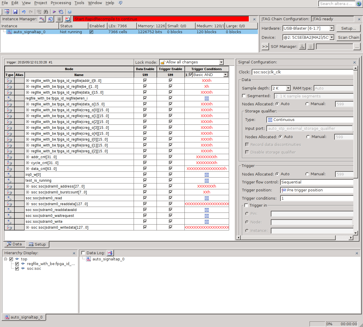
Save the file, add it to the project and perform a complete assembly.
After the end of the build, we need to get the .rbf file:
quartus_cpf -c etln.sof dma.rbf Everything, the firmware is ready. Go to the software part.
Attention: remember that after changing the settings in Qsys (in particular after turning on fpga2sdram ), you need to regenerate and rebuild the Preloader .
Also note that in the githaba for FPGA, only files with Verilog-code and a file with Qsys settings are laid out.
Project files (.qpf, .qsf, etc.) are missing due to the fact that they do not carry any really useful information.
Implementation of the userspace program
What do we need in order to work with the DMA controller from the software side?
First, we need to be able to configure and run a DMA controller. For this we use the mem program from the previous article.
Secondly, we need to get a memory area, the address of which we will be able to transfer to the DMA controller.
Here you need a small digression. Usually, all processes in userspace and even the majority in the kernel work with so-called virtual addresses. But the DMA controller needs to pass the physical address (more precisely, the bus address, but for the platforms we use it is equal to the physical one)
In the core for performing such tasks there is a set of special functions that allow you to get a physical (and vice versa) virtual address or allocate a memory area and get two addresses at once that point to it.
What to do in userspace ? We will be helped by a wonderful file / proc / [PID] / pagemap , which contains information about the mapping of all virtual pages to physical for any process.
Information for each page in this file is equal to 8 bytes. At the same time, the lower 55 bits contain the so-called physical page number - Page Frame Number ( PFN ), and the higher 9 bits contain various flags (page presence, being in a swap, etc.). A detailed description can be found here or in man proc
Thus, knowing the virtual address and page size, it is easy to calculate the virtual page number. After that, from the file / proc / [PID] / pagemap you just need to read 8 bytes at the desired offset and in the lower 55 bits will be the number of the physical page. And it is already easy to translate it into a physical address, which we will write to the DMA controller.
If our memory area starts on the page border, then everything becomes a little easier.
Therefore, instead of the malloc () function, it is better to use the posix_memalign () function, which allows you to set the desired offset.
Also, in order to prevent unloading data from RAM to swap, it is advisable to use the mlock () function
The things described above are performed by the phys_addr.c program .
Important note - pages adjacent to a virtual address space will not necessarily be contiguous in RAM.
Therefore, in this method, we cannot write data with a DMA controller that is larger than the page size.
We can get around this limitation when we write the driver.
Interim check
So, the firmware and test program are ready, time to test them a bit.
Copy the binaries to the SD-card, connect the USB-Blaster and run our board.
I wrote above that you need to enable the fpga2sdram interface before booting Linux . This is true, but not always.
If you turn on the interface already in Linux and try to read data from the FPGA in memory, the system will completely freeze.
But write the data work. Naturally, this option is clearly not to be used on the combat system and below I will write how to correctly initialize the fpga2sdram interface. But for intermediate testing, this is fine for us.
To get started, flash the FPGA:
cat dma.rbf > /dev/fpga0 Now enable the HPS-to-FPGA interface:
echo 1 > /sys/class/fpga-bridge/hps2fpga/enable If we start SignalTap now , we will see that the sdram0_waitrequest signal constantly hangs at 1. This is due to the fact that the fpga2sdram interface is turned off.
Turn it on:
./mem.o 0xFFC25080 0x3fff Writing units to the register bits 0xFFC25080 includes the corresponding ports of the fpga2sdram interface. A description of which bits for which ports are responsible is given in the above Handbook . For simplicity, we just need to include all the ports (a total of 14 bits are used in the register).
Now in SignalTap, the sdram0_waitrequest signal has become 0.
Run the phys_addr utility:
./phys_addr It allocates a buffer and displays its physical address. I have it 0x2d593000 .
We remember that when using the fpga2sdram interface, you need to be addressed by words.
Since the words are 128-bit, the address of the word is calculated as follows:
0x2d593000 / 16 = 0x2d59300 We write this address in the FPGA registers:
./mem.o 0xC0000002 0x2d59300 For the address we use control registers numbered 1 and 2. Each address is 16 bits or 2 bytes. Since the HPS-to-FPGA begins with the address 0xC0000000 , the first control register in the first control register will be 0xC0000002
Let me remind you that the mem.c utility uses exactly byte addresses.
After that, we write the length of the DMA transaction in control register number 3. The length should not exceed the page size, and for us it is 4096 bytes. Since our fpga2sdram interface is 128 bits wide, and we specify the size of the transaction in words, we have to write the number 256 in the third register:
./mem.o 0xC0000006 256 Next, we configure SignalTap to capture on the negative edge of the test_is_running signal and run the DMA controller.
To do this, write to the zero bit of the zero register first 0 (if it is not there), and then 1. At the same time, remember that the mem.o utility performs transactions of 4 bytes, and these are 2 of our registers. Therefore, if we are not careful, we wipe the data in the neighboring register.
So, we need to first read the data at 0xC0000000 , and then write them down, but with the zero bit set.
We read:
./mem.o 0xC0000000 I read 0x93000000
We write down:
./mem.o 0xC0000000 0x93000001 After that, we should get something like this in SignalTap :
SignalTap Result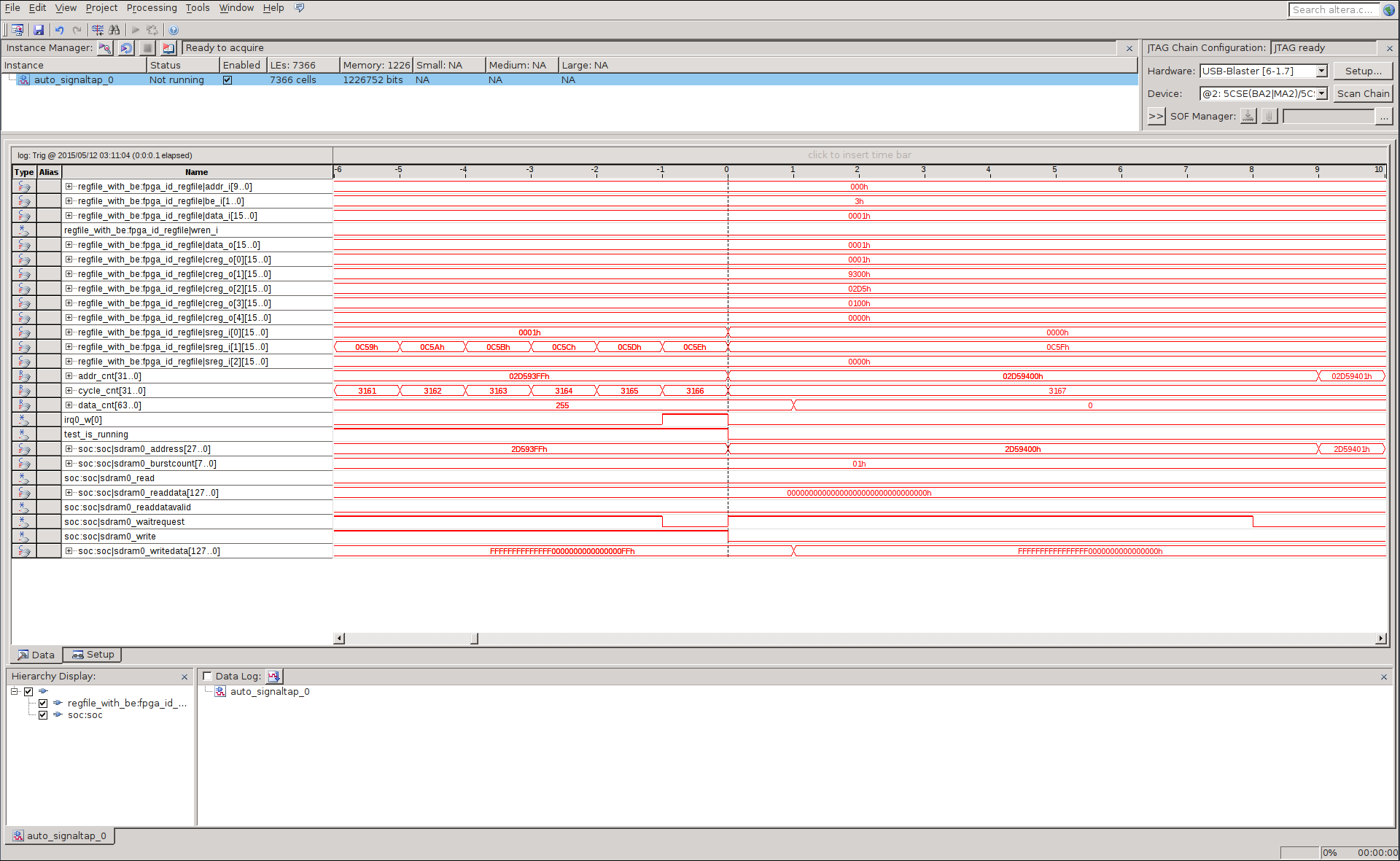
As you can see, the value of the cycle_cnt counter at the time of the end of the transaction is 3167.
Let's calculate the bandwidth. The frequency of the clock signal in my project is 150 MHz (to be able to change the frequency over a wider range, I do not use the clock from HPS, but import it there, I took it with the PLL. These changes are trivial, but they are not in the github).
Width - 128 bits. For 3167 cycles, 256 words were transmitted. Total:
128 * 150 / (3167/256) = 1551 /c UPDATE: Such a small bandwidth obtained due to a typo, details in the conclusions.
It remains to make sure that the data is recorded correctly. “Remove” the phys_addr utility from a pause by pressing Enter.
We should see this text:
Phys_addr execution result
0: 0x0 1: 0xffffffffffffffff 2: 0x1 3: 0xfffffffffffffffe ... 507: 0xffffffffffffff02 508: 0xfe 509: 0xffffffffffffff01 510: 0xff 511: 0xffffffffffffff00 If you saw, then everything went well.
Having experimented with different parameters, I saw that the frequency of the clock signal has almost no effect on throughput.
It remains approximately the same as for 25 MHz, which is for 150 MHz.
But the width of the fpga2sdram interface , on the contrary, gives an almost linear relationship - tested at 64 and 128 bits. For 256 did not check.
Naturally, due to the fact that the amount of recorded data is small (only 4096 bytes), the measurement error is quite large.
We can increase the size of the DMA transaction by writing our primitive driver.
Driver writing
The article came out a little more than I expected, so I’ll tell you about the driver very briefly.
Especially because with him we still have to work in the following articles.
But the code is on a githaba who is interested - you can see the details.
The basic idea is simple - when launching the driver, we set the parameter what size of the transaction we need.
The driver allocates memory and writes the bus address and transaction size to the FPGA.
The driver also registers an interrupt handler, which we specified in the FPGA firmware.
After this, the driver creates two char devices:
- / dev / etn-ctrl - to run a DMA transaction
- / dev / etn-data - to get data
When reading from the / dev / etn-ctrl file , a DMA transaction starts.
After that, the call is blocked until the arrival of an interrupt from the FPGA.
When the interrupt arrives, the call ends. This means that the data is written and can be read from the / dev / etn-data file .
For the driver to work in the .dts file, add the following lines:
Changes to .dts
fpga { compatible = "mtk,etn"; interrupts = <0x0 0x28 0x1>; }; The first line specifies a compatible driver, and the second line indicates the number and type of interrupt from the FPGA.
When using a transaction of 4MB in size, the bandwidth goes to about
findings
A primitive DMA controller was written in the FPGA and its throughput was measured.
UPDATE:
The small bandwidth is due to a typo in the DDR3 settings.
Namely, the fact that the PLL clock was set to 125 MHz, and not 25 MHz, as it really is.
Because of this, the multiplier and divider coefficients for the PLL were calculated incorrectly.
As a result, DDR3 worked at 66 MHz instead of the 333 MHz.
With the correct coefficients and interface width of 256 bits, the bandwidth is about 16-17 Gbit / s, which corresponds to the theoretical for the DDR3 interface with a width of 32 bits and a frequency of 333 MHz.
I will describe in more detail in the next article.
A further outline of the articles is this, if, of course, they are interesting to someone:
- Implementing the framebuffer for ILI9341 in FPGA
- Working with SGDMA Controller
- Implementing a gigabit 2-port NIC in FPGA using an SGDMA controller
Thanks to those who got to the end! Good luck.
Source: https://habr.com/ru/post/248145/
All Articles