Core PCI-express in Achronix FPGA - quick start
This post was written to show developers of FPGA design how to start working with the PCI-express bus on the Ahronix Speedster22i platform with the least amount of time and effort. The article describes the organization of the project, the adaptation of which to the specific requirements of the developer is reduced to a simple modification of the source text of just one module, which allows you to connect to the host's PCIe bus in literally 1 hour. Hopefully, developers on other platforms will find this article just as interesting.
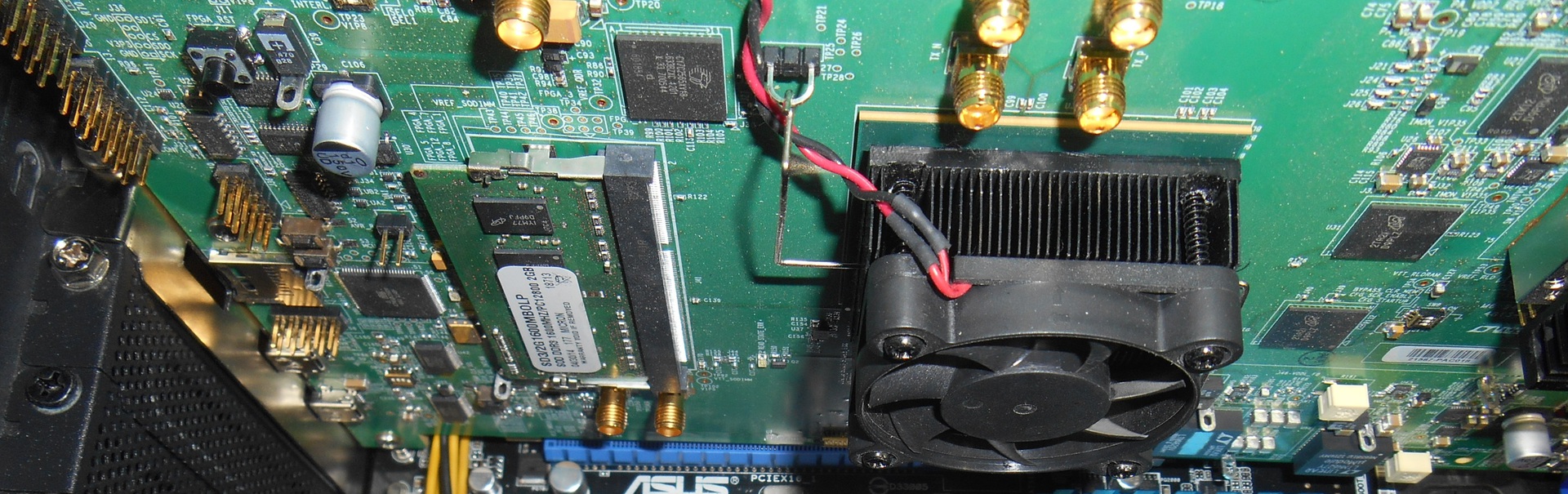
The Speedster22i HD1000 FPGA has two PCIe hardware cores certified by PCI-SIG compliant with the PCIe 3.0 specification, and the Speedster22i HD1000 Development Kit (which I wrote about in a previous post ) has one of these cores connected to the PCIe connector. Through the PCIe interface it is very convenient to interact with the debug board with the host computer. In fact, this is the only high-speed solution for this purpose. An alternative to using PCIe for communicating a debug card with a host computer can only be the built-in com port, which is several orders of magnitude slower. All other solutions require more or less hardware sophistication; at a minimum, signal level converters will be required.
Achronix has a reference design that demonstrates how the PCIe hardware core works in all its glory - the kernel works in target mode with access both to the CPU itself and through the DMA mechanism for reading and writing. I checked, everything works fine. But this design turned out to be quite difficult to modify for its own purposes due to insufficient modularity and excessive complexity of the code in the Verilog language . Therefore, it was decided on the basis of corporate design to create your own version, removing from it everything related to the exchange via DMA , as well as structuring it in such a way as to explicitly select in it modules with unchangeable code and modules whose code needs to be modified in order to adapt to specific tasks of the developer. The result was a simple, well-structured project, the adaptation of which for the specific tasks of the developer comes down to a simple change in the code of just one module.
Achronix's FPGA feature is the presence of hardware-implemented IP cores of controllers of such interfaces as PCIe , DDR3 , 100/40 / 10G Ethernet and Interlaken . These hardware cores provide everything that is necessary for the operation of these interfaces, the only thing that is required of the developer is to write your own interface modules with these controllers. As a result, the amount of work is dramatically reduced. In addition, the achievement of the required timing is greatly simplified. In the case of a PCIe design, it took just a few interface modules, most of which were taken from proprietary reference design.
')
Brief description of the project
The project has access to three 128-bit registers. The PCIe core is configured for 3 BARs: BAR0 - 64KB, BAR1 and BAR2 - 8 KB each. Access to registers is carried out through BAR1. The presence of 3 BARs is due to compatibility requirements with the driver used. A description of the registers is given below:
| Name | Offset in AP BAR1 | type of | Description |
|---|---|---|---|
| R0 | 0 | RO | {4 {32'hDEADBEEF}} |
| R1 | 20h | Rw Rw | Bits [7: 0] - output to the line of LEDs Bits [127: 8] - not used |
| R2 | 40h | RO Rw | Bits [7: 0] - reading the switch range Bits [127: 8] - not used |
When upgrading the project, the first thing that was done was to delete the code associated with the exchange of data through DMA . After that, the read and write channels target_read and target_write were used to connect to the kernel. Further, the structure of the modules shown in the figure was determined:

A total of 4 modules turned out (some of them include submodules)
The composition of the modules:
- pcie_g3x4.v is a wrapper for the PCIe hardware core. It determines its parameters, such as VendorID , the number of lanes, the width of the local bus, etc. This module is generated using the kernel of the ACE development environment.
- pci_target_bus_ctrl.v is a wrapper module that matches the target channel of the hardware core and the local bus on which the registers are located that are accessible via the PCI bus . Since the target channel consists of two independent subchannels: write and read, this module combines two modules: pci_target_bus_write_ctrl.v and pci_target_bus_read_ctrl.v , implementing write and read operations, respectively.
- lbus_registers.v is the module containing the user registers themselves. The only module that requires modification of the code for a specific project.
- ACX_SNAPSHOT.v is an auxiliary module for in-circuit debugging. At the end of debugging can be excluded from the project.
In this project, to achieve the necessary developer functionality, it is required to change the source code of just one module - lbus_registers.v . All other modules are used as is, without any alteration. At the same time, the lbus_registers.v module can be used as a template to which the developer needs the functionality. Thus, in order to get a working interface with several registers on a PCIe bus , the time required to write the module code is no more than an hour.
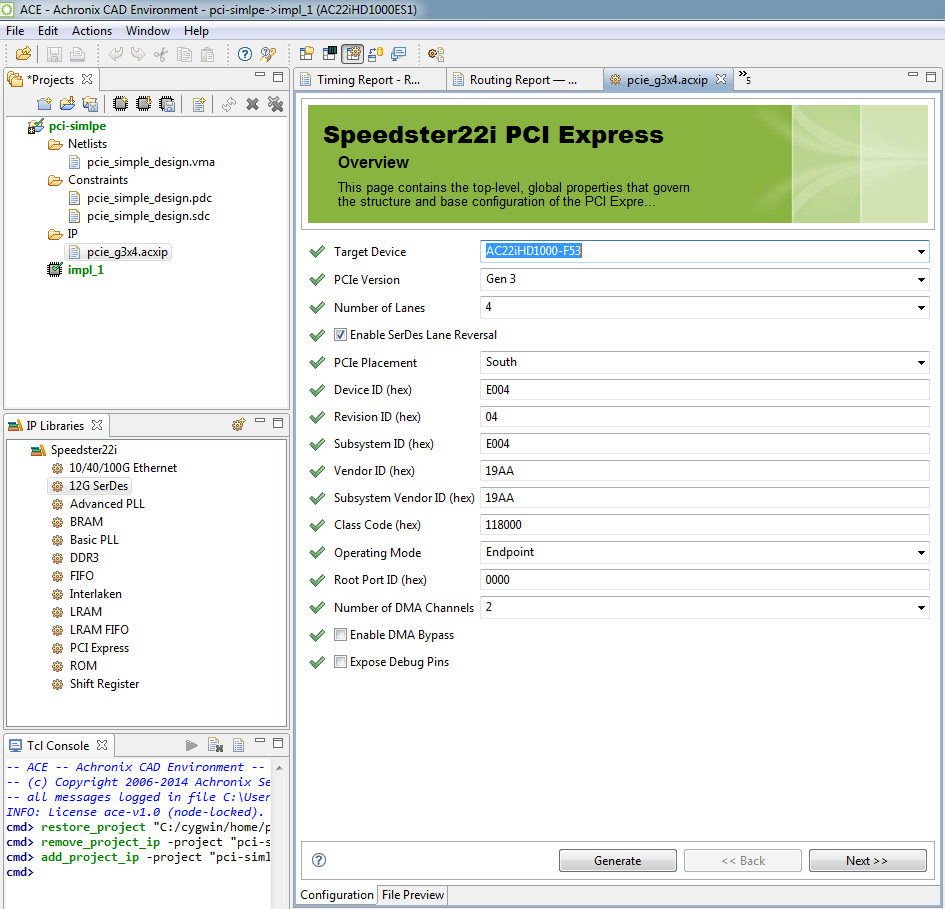
PCIe kernel generation
To generate a kernel, you can use the ACE shell generator. All specified parameters are saved in a file with the .axip extension, which can be edited at any time. The result of the generator are text files in Verilog and VHDL . A screenshot of the kernel generation process is shown below:
Pcie kernel target interface
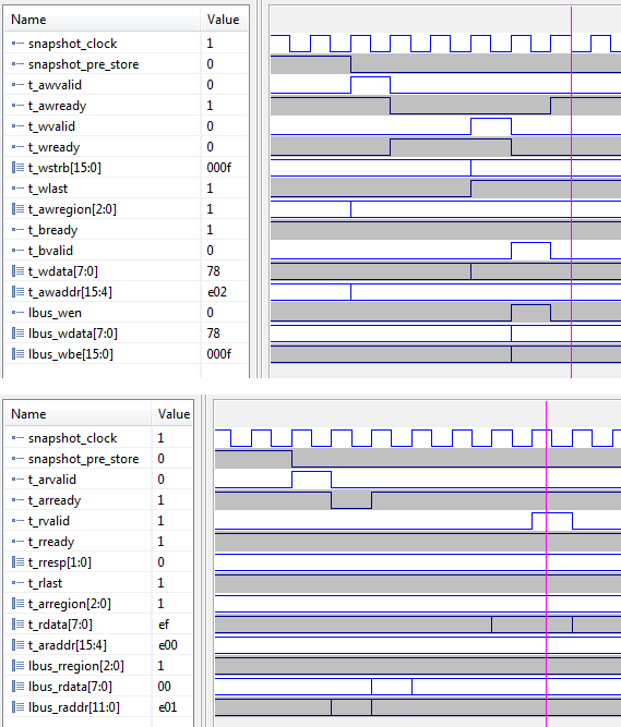
The PCI hardware core includes several interfaces, but we are interested in the target interface. Registers acting as passive devices are connected via this interface, and the processor acts as an active device. The target interface consists of 4 channels: set the write address, write data, set the read address and read data. The writing and reading channels operate independently of each other. Below are timing charts of write and read transactions. The same diagrams show local bus signals.
Local bus
The local bus has a very simple structure. It consists of two independent channels - writing and reading and can be configured to different word widths. This project uses 128-bit words.
The local bus interface implemented in the lbus_registers.v module provides for writing to the registers without delay and reading with a delay of 1 clock cycle. The real delays, however, are somewhat higher, since submodules included in the pci_target_bus_ctrl.v module contribute to the latency of write and read transactions.
Implementation
The implementation of the project consists of two stages - the synthesis phase and the trace phase.
Directory structure
The following directory organization was chosen for implementation:
 pci_simple
     | --- src
     | --- syn
     | --- tr
     | --- tools
The src directory contains source files in the Verilog language . The syn directory contains the files needed for synthesis using the synplify program, and the tr directory contains the files needed for the trace step. Also in this directory by default are generated kernels. The tools directory contains drivers and the PciExpress program, which can be used to read and write data to the registers connected to the PCIe bus .
Synthesis
The syn directory contains the pcie_simple_design.prj project file . This file must be indicated by the synopsys synplify-pro synthesis program. The result of this program is the pcie_simple_design.vma file in the syn / rev_1 subdirectory . This file is input to the next stage - tracing. A screen shot during the execution of the synthesis step is shown below:

Tracing
The tracing step is performed by Achronix’s own ACE program. The tr directory contains the pci-simple.prj project file, which must be specified by the ACE program. At the end of the tracing step, the pci-simple-design.jam firmware file will appear in the tr / impl_1 / output subdirectory , which is loaded directly into the FPGA. Screenshot during tracing step:

The counters
There are only two files of constraints - one describes the clock circuits, and the other defines the I / O pins used. The files are in the tr directory and have the names pcie_simple_design.sdc and pcie_simple_design.pdc, respectively. They are already connected through the project files to the synthesis and trace programs.
results
Timing
| Trace results | |||
|---|---|---|---|
| Frequency (MHz) | |||
| Clock / Group | Target | Achieved | Meets timing |
| user_clk | 212.5 | 308.5 | yes (+ 45.2%) |
| core_clk | 212.5 | 433.5 | yes (+ 104.0%) |
| sbus_clk | 50.0 | 138.7 | yes (+ 177.5%) |
| Tck | 10.0 | 175.4 | yes (+ 1653.6%) |
We are interested in the user_clk clock group to which the user registers are connected. As can be seen, at a given frequency of 212.5 MHz, a result of 308.5 MHz was achieved, i.e. 45% higher than required.
Recycling
| Resource | Busy |
|---|---|
| RLBs | 0.520% |
| LUT4 Sites | 0.410% |
| DFF Sites | 0.520% |
| MUX2 Sites | 0.010% |
| ALU Sites | 0.170% |
| LRAM Sites | 1.280% |
| BRAM Sites | 0.190% |
| BMULT Sites | 0.000% |
| I / O Pad Sites | 1.980% |
| Data pads | 1.740% |
| Clock pads | 12.50% |
| Reset pads | 0.000% |
Connect to host computer
A driver is required to connect to the host computer. Under certain conditions, you can use the driver from the corporate reference design. With this driver, the application PciExpress.exe works , through which you can access registers connected to the PCIe bus . To be able to use these tools, you need to preserve the structure of the BARs of the original design and save the values of the VendorID and DeviceID parameters.
To start working with a Windows host computer, you must perform the following steps:
- Connect the debug board to the computer via the PCIe bus . Requires a PCIe x8 slot or wider. Connection should be made on switched off devices in compliance with antistatic protection measures. The debug board is powered from an external power source.
- Turn on the power of the computer and the board. The power on procedure is not significant.
- Download firmware to FPGA.
- Using the device manager, find a new device on the PCI bus and install a driver for it.
- Reboot
- After rebooting, using the PciExpress program, you can write / read registers.
The following figure shows the result of reading the register with an offset of 0 in the address space BAR1:

Customization of the lbus_registers.v module
In order for the source code to be used in your own projects, you need to enter into the design the registers needed by the developer. All user registers are in the lbus_registers.v module and when customizing it, the following simple steps are required:
- Write code for each user register
- Set the address of each register in the parameter list
- Write the address decoder code for each register
- Connect each register to write and read buses
We show how to implement these actions in practice.
• Define the register name and its length:
reg [AXI_DATA_WIDTH-1:0] my_register; • Define the read and write gates for this register:
wire selw_my_register; wire selr_my_register; • Write an always-block for this register. This is conveniently done using the generate statement.
In the simplest case, the code looks like this:
genvar i; generate for (i = 0; i < AXI_BE_WIDTH; i = i + 1) begin: leds_lanes always @( posedge clk or negedge rst_n ) if (!rst_n) my_register [7+ 8*i: 8*i] <= 8'h0; else if (selw_my_register && lbus_wr_be[i] ) my_register[7+ 8*i: 8*i] <= lbus_wr_data[7+ 8*i: 8*i]; else my_register [7+ 8*i: 8*i] <= my_register [7+ 8*i: 8*i]; end endgenerate If more complex processing of individual bits is required, then the always-block will naturally become more complicated and it may be easier to write the code explicitly without using the generate statement.
• Add a line to the list of parameters:
parameter ADDR_MY_REGISTER = 32'h1234_5678 ,where - instead of 32'h1234_5678 we specify the real offset in bytes in the required address space
• We write formulas for register selection signals:
selw_my_register = reg_wr_hit & (lbus_wr_addr[REG_ADDR_WIDTH-1:0] == ADDR_MY_REGISTER [REG_ADDR_WIDTH+AXI_REMAIN_WIDTH-1:AXI_REMAIN_WIDTH]); selr_my_register = reg_rd_hit & (lbus_rd_addr[REG_ADDR_WIDTH-1:0] == ADDR_MY_REGISTER [REG_ADDR_WIDTH+AXI_REMAIN_WIDTH-1:AXI_REMAIN_WIDTH]); • In the always_comb block
always_comb begin case (1'b1) … endcase end Add a new branch inside the case statement:
selr_my_register: c_reg_rd_data = my_register; The above steps are repeated for each user register.
Module interface
The module interface is defined as follows:
module lbus_registers #( parameter BAR_NMB = 3'd0 parameter AXI_DATA_WIDTH = 128, parameter AXI_BE_WIDTH = AXI_DATA_WIDTH/8, // AXI Len Width parameter LBUS_ADDR_WIDTH = 12, // 64 KB expected for NWL Reference Design parameter REG_ADDR_WIDTH = LBUS_ADDR_WIDTH, // 64 KB expected for NWL Reference Design parameter ADDR_R0 = 32'h000_0000, parameter ADDR_R1 = 32'h000_0020, parameter ADDR_R2 = 32'h000_0040 ) ( input wire rst_n, input wire clk, // input wire [7:0] switches, output wire [AXI_DATA_WIDTH-1: 0] rg1_out, output wire [AXI_DATA_WIDTH-1: 0] rg2_out, output wire [71: 0] debug_bus, // Local Bus channel input wire [LBUS_ADDR_WIDTH-1:0] lbus_wr_addr, input wire [2:0] lbus_wr_region, input wire lbus_wr_en, input wire [AXI_BE_WIDTH-1:0] lbus_wr_be, input wire [AXI_DATA_WIDTH-1:0] lbus_wr_data, // input wire [LBUS_ADDR_WIDTH-1:0] lbus_rd_addr, input wire [2:0] lbus_rd_region, output wire [AXI_DATA_WIDTH-1:0] lbus_rd_data ); Settings
The settings for the lbus_registers.v module are listed in the table:
| Parameter name | Default value | Value range | Description |
|---|---|---|---|
| BAR_NMB | 3'd0 | 3'd0-3'd7 | BAR number to which the address selector is configured |
| AXI_DATA_WIDTH | 128 | 128, 256 | Data bus size |
| AXI_BE_WIDTH | AXI_DATA_WIDTH / 8 | - | Do not change manually |
| LBUS_ADDR_WIDTH | 12 | 8-15 | Specifies the local address bus width. Usually corresponds to the size of the AP of the largest BAR |
| REG_ADDR_WIDTH | LBUS_ADDR_WIDTH | <= LBUS_ADDR_WIDTH | Sets the bit depth of the local address bus AP corresponding to the selected BAR |
| ADDR_R0 ADDR_R1 ADDR_R2 | 32'h000_0000 | Depends on BAR size | Register address R0 (R1, R2). Register addresses are always specified in bytes and correspond to their offset in the address space of the BAR |
Debugging
Debugging is performed using an internal signal analyzer, for which the project uses the ACX_SNAPSHOT.v module, which is enabled by the conditional compilation directive `define USE_SNAPSHOT . Documentation on the organization of in-circuit debugging is located on the Achronix website in the Snapshot User Guide.pdf file.
Conclusion and conclusions
Even such a difficult task as connecting to the PCI-express bus is solved on the Achronix Speedster22i platform easily and, most importantly, quickly. Creating a working project based on the PCIe hardware core was not easy, but very simple.
The story about other hardware cores of the Achronix Speedster22i FPGA is planned as they are learned. In subsequent posts will be told about the core DDR-3 and 100G Ehernet .
Links
1. Achronix announces the compliance of its PCI Express hardware cores in the FPGA Speedster22i to the PCI-SIG specification (English) www.achronix.com/wp-content/uploads/pr/2014_May_PCI-SIG.pdf
2. HD1000 dev kit debug board (English) 22iHD1000_Development_Board_Schematic.pdf
3. Guide to using PCIe controllers on Speedster22i (English) www.achronix.com/wp-content/uploads/docs/Speedster22i_PCIe_User_Guide_UG030.pdf
4. Snapshot User Guide (English) www.achronix.com/wp-content/uploads/docs/Speedster22i_Snapshot_User_Guide_UG016.pdf
5. Original reference design: Speedster22i_PCIe_Demo_Design.zip
6. The source files of the described project: drive.google.com/file/d/0B9Gt8fTYH6s-VGhfbk5RQWM4bk0
Source: https://habr.com/ru/post/244997/
All Articles