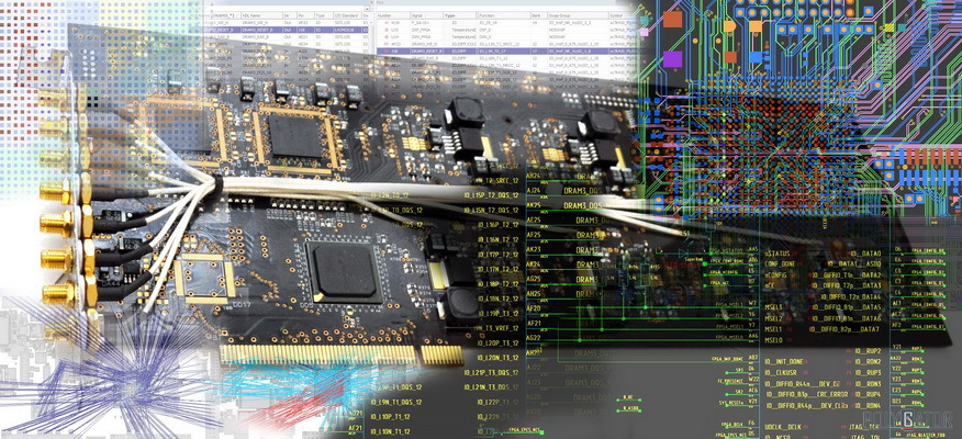
Scheme> board> FPGA
On Habré there are articles for beginner FPGAs, there are articles with reviews of the PCB tracers. I already referred to some of them in my first article about the creation of printed circuit boards . In the second article about SimBank in the comments I had a dialogue about the complexity of developing FPGAs and supporting projects with it. It has been suggested that it is easier to assemble several simple devices instead of a single one. Sometimes it's really easier. When it comes to two, four, eight devices. The series can be continued with the frequency you are used to. To overcome the threshold of comfort. Two is a bunch? And what if there is a wish for 100 or 200 devices of the same type?
To use or not to use FPGA in this or that problem, everyone decides on his own (or with colleagues).
Today I want to bring to your attention an article about the features of creating a PCB with FPGA. We take the tool “IO Designer” from the company Mentor Graphics as a basis.
Someone may be useful material, someone just interesting, but someone may not agree with me.
For some CAD systems, for example, Altium Designer, updates with the bases of new microcircuits periodically come out. (If you are a subscriber for updates). For Cadence and OrCAD, component manufacturers often lay out the library elements of circuit symbols and cells for printed circuit boards. For ExpeditionPCB from Mentor Graphics, this luxury is the exception rather than the rule. About PADS (another product for the end-to-end design of printed circuit boards from Mentor Graphics) I will not say, I did not have to work with it. In the design system itself is a very convenient library component manager. There is a very successful “LP Wizzard” program for building footprints of components for printed circuit boards in accordance with the requirements of the IPC-7351 standard. (Land pattern wizzard). To create graphic schematic symbols of simple and not-so-many components, it is possible to import from a file. And for FPGA, there is an “IO Designer”, which combines the symbolic, schematic, paid (from the printed circuit board) and Verilog (VHDL) parts of the project.
IO Designer contains a knowledge base about most FPGA and CPLD of such FPGA manufacturers as Xilinx, Altera, Lattice and Acctel. Along with the release of new families from the FPGA manufacturers, MG releases updates to the FPGA databases. But the new documentation on the microcircuit families will still have to be studied.
Suppose we chose FPGA, studied (familiarized) its features and are ready to create.
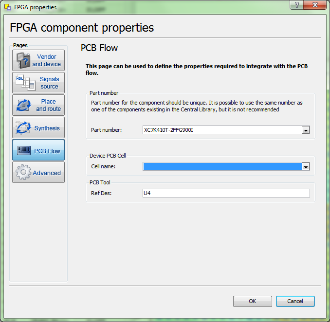
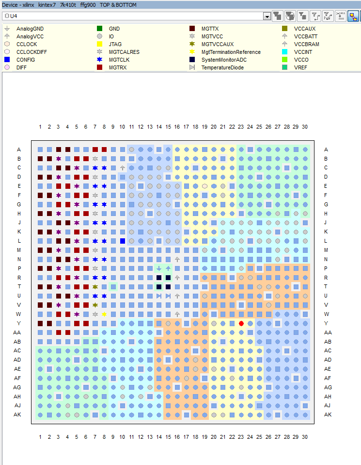
When creating a project, we can choose the FPGA manufacturer, the FPGA family, the type of body, and the number of elements. And also specify the speed of the components (to set the exact Part Number).

In FPGAs, most contacts can be configured, both on the output and on the input. At first glance, connect - I do not want. This is where we bring the SD card controller, here is the RGMII for Ethernet PHY, and so on. That was not the case. With such a bold detour of contacts for convenience, we can stumble upon a mass of pitfalls. Reading the documentation will avoid most of them, but it will not make it easier to assign contacts. And the project of the board can turn into a continuous mess.

In this image, everything is not so bad, because it was created “artificially” on the basis of a well-developed project. It’s usually not so smooth the first time. And at the stage of adding FPGA, not all elements are placed on the board. But it is specially noted that the signals from the lower left connector do not come to the lowest corner of the FPGA. As a result, they intersect with other signals and, when tracing, may require both additional vias and additional board layers. As a result, will increase the cost of production.
The ability to customize contacts is also very limited. It is good if our board is created for one specific product. There are conclusions of adjacent elements, we create response buses / signals for them in the FPGA. Launched a trial project in CAD for FPGA. If everything succeeds, then you can give it to the trace.
As a digression: EMNIP on Xilinx Spartan-6 were specially assigned pins for DDR memory, which were then conveniently traced with the proper mutual placement of chips on the board. And there was no need to move them afterwards.
')
Often, according to the TOR, it is necessary to create some kind of versatility and our fee will be used for several projects in the future. We have so designed a central board with a processor for working with many other devices, a kind of debug board with FPGAs, a processor and an OS “for our own”. And there is a lot to be foreseen. Leave, if you need one contact on the connector to feed the clock, or to output a signal from the PLL. Determined with the directions of the signals on the bus: input, output or bidirectional. If we have a central board is always a master, then such signals to the address bus or managers can be made only at the output.
If we have a response from a slave board like WAIT or BUSY on the bus, then on the master board, you can assign them to outputs that can only be inputs. You can also do with the findings determine the presence of the board.
Such a mission, at first glance, limits the possibilities for subsequent tracing and shuffling of signals. But as practice shows, it is better to know such restrictions in advance. And not just assign all the signals “Inout”.
We can select a file from which to draw a list of signals. This can be a test project, a file on Verilog or VHDL.

If the trial project has not been done yet, then we can not specify such a file. And then just create signals in the program window. Types of signals by default. For single signals and for differential.
Next, we can assign a place where we will then upload the file with our location of contacts.
Then you need to decide how we want to work with the scheme, whether we need full-fledged symbols or just create chains in the circuit design, and the descriptions of all contacts will be transmitted only as an exchange file with CAD FPGA.
I always liked the option when you do not need to create schematic elements, and all exchanges go through unknown internal paths. But, working in a team, one has to accept more mundane rules of the game. Thus, according to the corporate standard for the design of schemes, I always had to divide the symbol by bank, separate configuration chains, land, power, and others. There are pros in this division, but there are also disadvantages. Circuit symbol had to do me. For a FPGA with 484 contacts, it is not so difficult to make a schematic symbol correctly, as it may seem to someone. But for a chip with 1172 contacts, this activity is very tiring. Most contact names have long and similar names and are easily confused. You can generate all the characters automatically. But then they do not coincide with the "corporate" preferences. In IOD, you can easily create a symbol in the database of elements simply by dragging the mouse from the contact list window to the symbol window. I will not say that it is also just like playing the “Farm Farm”, but at this stage we can simply assign signals to the contacts of the microcircuit with the mouse. In this case, you can specify how to designate the name, functional purpose, contact number or in its own way. I usually choose a display by function. Since, in my opinion, this name is more informative and then the diagram shows what kind of signal you can get here.
From the observations I can note that the latest names for Xilinx (for families of the 6th and 7th series) are quite meek and informative.
IO_L6N_T0_VREF_13
IO - I / O pin
L6N - designation of a differential pair
T0 - byte designation inside which you can swap data signals for memory (this point needs to be clarified!)
VREF - an external reference voltage can be supplied here if the standard of the selected signal for the bank requires it and there is no possibility to connect it inside the FPGA.
13 - bank number.
Altera also sometimes comes across normal functional designations, but more often (my subjective opinion) difficult-to-reproduce contact names, which then do not fit on the sheet with the scheme. Perhaps, if I made circuits with large amounts of memory, multipliers, or some colliders, I would need such a name.
IO_DIFFIO_T18p__DATA15_DQ3T0_X9__DQ3T9_X18_DQ5T27_X36
In this case, it helps to specify a Custom Label for the contact name. And enter the necessary name with your hands. I usually copy the functionality and reduce it to the form
IO_T18p_DATA15_DQ
In this case
IO - can be used for I / O signals
T18p is the number of the differential pair in the upper segment.
DATA15 - this contact can be used for parallel loading of the configuration.
DQ - tells me that this is an abbreviation of the functional purpose of the contact (there may still be DM and DQS)
This is one example of how a contact can be called on the basis of its functionality and for any particular project, some other sign will be displayed in the first place.
So, for example, with Altera, when using LVDS signals, you need to use an external load. For some banks, this is a load resistor only on the receiving side, and for others it is also needed at the output. This can be noted on the schematic symbol in the Custom Label property. The same applies to PCI signals type. Not all banks can be assigned standard bus 3.3V-PCI. And this can also be noted on the symbol. Despite the ever-increasing displacement of its standard PCIe in desktop systems, in the industrial performance, it is still popular. And some customers are looking for devices in this version.
You can add an inscription in the symbol for all contacts at once. This will reduce the amount of text inside the symbol. Since any additional information will overload the symbol and scheme, a compromise is needed here. I did this for Xilinx microcircuits, which have microcircuits that are compatible with the contacts inside one case with a different number of logic elements, but some of the contacts are not involved in the “small” microchips. Then, in the project, a part of the circuit was not soldered and it was possible to put a more “light” chip. Given this in the distribution of contacts, then you can save on the missing components and the price of the FPGA.
For convenience, I make banks-split characters. An exception can be made for contact configuration. If the project has a complex synchronization structure, then the CLK inputs — local, global, and others — can be assembled into a separate symbol. The power contacts of the VCCO banks are placed on the symbol with the bank or on a separate one - at the request of the PRIME developer.
Contacts power core, VCCAUX, land and other things, most often, stand on separate characters.
Allegedly, it is now possible for all power contacts to create only a circuit in the circuit and not to overload the circuit with a large number of contacts of the same type. We have not done so, so I am not familiar with such options. This can be found in the reference documentation or from webinars and online training materials on the site of Mentor Graphics and its representatives.
I transmit the created symbols directly to the design of the circuit, indicate the type of the enclosure, annotate the board and the chip is attached to the board, the circuit and the IODesigner.
Creating and assigning signals
As described above, we can export signals from a file or create them ourselves.
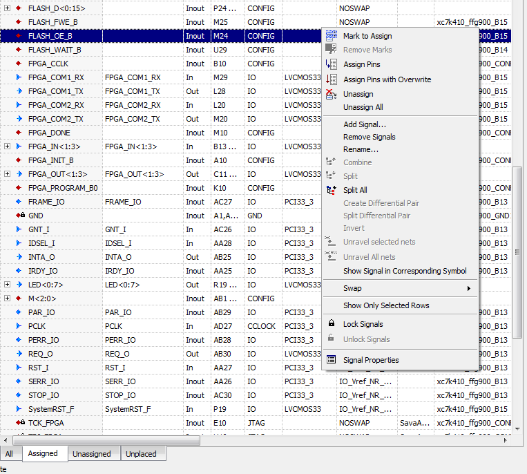
Signals can be assigned either by mouse or via import / export. By pressing the SHIFT, CTRL or ALT keys you can reassign signals to already assigned contacts. Or assign all selected signals to one bank. Visually, banks are displayed in different colors. Contacts of different types are displayed with different icons. You can enable the display of differential pairs. Over time, busy signals will be painted over.
We update the scheme and see the symbols on the diagram already with signals.
See how they are connected on the board. This is usually already shown above “porridge”.
Sometimes I immediately make a simple list of signals so that they are automatically created in the system, then I drag them to the circuit editor to other elements.
There is an option to import the list of signals from the scheme.
By synchronizing the design of the scheme, the board and the IO Designer, we can trigger the display of signals in the IO Designer window. With reaching chains from FPGA to the components connected to it.
Now we can comb our signals. And all this will be done automatically in accordance with the rules introduced by us. Configuration signals will not go anywhere. We can also pre-fix the signals to prevent a change in their location.

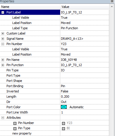
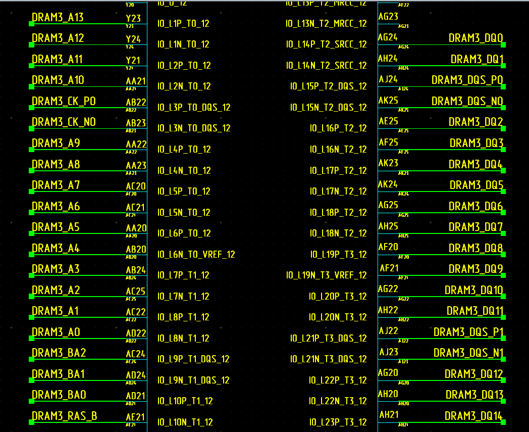
Please note that the DRAM3_RESET_B signal, to which the input / output standard LVCMOS_1.35V must be assigned and it cannot be located in the same bank with SSTL standard signals, is assigned to bank 17, and all other DRAM3 * signals to bank 12. As in the system Since only four signals with LVCMOS_1.35V, they are assigned the standard LVCMOS1.8V and supplied with a level converter.
Despite the seeming confusion of the signals, they are now straightened out in accordance with the rules assigned. For the convenience of working with the project in Quartus.
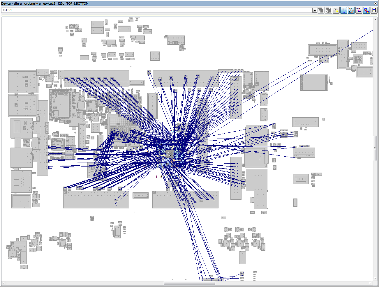
The image shows the placed components, and the lines drawn to them from the FPGA. Sometimes, if not all components are placed, it is impossible to expand all contacts for the first time without a trace. Although it all depends on the task.
After such a distribution of contacts, it is already possible to return the circuit to the final trace, or to trace it yourself.
You can also export to Verilog / VHDL file. We can export to * .ucf, * .pin or another file. To give it to the FPGA designer for a trial project, suddenly something was not taken into account. But in a small team it is not always possible to do this right away due to the heavy workload of other projects. (Old improvements, new wishes of customers or parallel projects).
Limitations.
This method has limitations, which I do not always know how to get around. But basically they are connected with the need to do a lot of things for versatility and in reserve. We have to invent crutches and stuff. So with Altera, by default, the differential signal should not be located near the differential signal. The compiler will issue a warning. We can bypass it by setting the parameter SLEW_RATE = 0 MHz in Pin Planner Quartus. After which the compilation will complete successfully. Even if in fact we have the signal will hang with a frequency of 20 MHz. There is no such parameter in IODesigner. As a result, on the diagram, these contacts are used by the latter or I set the type of signal to them so that it does not cause a conflict, for example, a PCB signal or a configuration one.
There are other limitations that are usually bypassed. But in general, I have a positive attitude towards them, since they force me to once again look into the documentation on the microcircuit much earlier than the ready payment arrives.
For those who work in other design systems, some things may not seem obvious and perhaps not necessary. So, as far as I know (heard), Altium allows you to customize the compilation of the project for the FPGA right in the project with the circuit and the board. I am not aware of all its capabilities. And for people who design it, they do not need import into Quartus or ISE. But we have a project of the printed circuit board is made by one person, projects for the FPGA by other people. When I give the circuit for tracing, I try to describe the signals as correctly as possible, while giving the PCB designer some freedom of action to change the contacts. We agree on any warnings that occur as they accumulate.
Finally, I would like to say that “IO Designer” is not a panacea. It does not turn the design of the circuit, board and project on the FPGA into an interactive game and does not exempt from studying the documentation on the chip. But working with such a tool is much more pleasant. The article does not describe all of its benefits. Also, I can not judge the completeness of libraries for all chips, since I only had to work with some of the Altera and Hilinx families. C Lattice I somehow managed to work a little bit on the debugging kit, but it didn’t get to the scheme, and even less to the board. With Actel, I did not work at all. From the comments on Xilinx, I can note that in my version there is no direct transfer of the file restrictions to / from Vivado. Maybe with the updates will be released. But since I am not leading the FPGA Xilinx project, I didn’t understand exactly what the problem was. We managed export through a * .csv file.
This publication does not claim to be a textbook on “IODesigner”, for this there are many lessons from Mentor Graphics. I know that in Russian the training is conducted by the company Megratek. www.megratec.ru .
Also, as far as I know, Mentor Graphics is preparing to introduce to the market xPedition - a new version of the design system. What is there to add specifically on IODesigner ʻu time will tell. Of those presentations that I saw, I was impressed by the update of the 3D display in the boards and the design of devices with several boards in one project.
Also, besides the CADs I mentioned, there are others for printed circuit boards. Each one has a list of advantages and a list of “what in Y is lacking as in X”. And if I did not name their advantages in comparison with the option of working through IOD - do not be offended. You can write about it in the comments. Or an article about how you design FPGAs in your CAD system.
To use or not to use FPGA in this or that problem, everyone decides on his own (or with colleagues).
Today I want to bring to your attention an article about the features of creating a PCB with FPGA. We take the tool “IO Designer” from the company Mentor Graphics as a basis.
Someone may be useful material, someone just interesting, but someone may not agree with me.
For some CAD systems, for example, Altium Designer, updates with the bases of new microcircuits periodically come out. (If you are a subscriber for updates). For Cadence and OrCAD, component manufacturers often lay out the library elements of circuit symbols and cells for printed circuit boards. For ExpeditionPCB from Mentor Graphics, this luxury is the exception rather than the rule. About PADS (another product for the end-to-end design of printed circuit boards from Mentor Graphics) I will not say, I did not have to work with it. In the design system itself is a very convenient library component manager. There is a very successful “LP Wizzard” program for building footprints of components for printed circuit boards in accordance with the requirements of the IPC-7351 standard. (Land pattern wizzard). To create graphic schematic symbols of simple and not-so-many components, it is possible to import from a file. And for FPGA, there is an “IO Designer”, which combines the symbolic, schematic, paid (from the printed circuit board) and Verilog (VHDL) parts of the project.
IO Designer contains a knowledge base about most FPGA and CPLD of such FPGA manufacturers as Xilinx, Altera, Lattice and Acctel. Along with the release of new families from the FPGA manufacturers, MG releases updates to the FPGA databases. But the new documentation on the microcircuit families will still have to be studied.
Suppose we chose FPGA, studied (familiarized) its features and are ready to create.
When creating a project, we can choose the FPGA manufacturer, the FPGA family, the type of body, and the number of elements. And also specify the speed of the components (to set the exact Part Number).
In FPGAs, most contacts can be configured, both on the output and on the input. At first glance, connect - I do not want. This is where we bring the SD card controller, here is the RGMII for Ethernet PHY, and so on. That was not the case. With such a bold detour of contacts for convenience, we can stumble upon a mass of pitfalls. Reading the documentation will avoid most of them, but it will not make it easier to assign contacts. And the project of the board can turn into a continuous mess.
In this image, everything is not so bad, because it was created “artificially” on the basis of a well-developed project. It’s usually not so smooth the first time. And at the stage of adding FPGA, not all elements are placed on the board. But it is specially noted that the signals from the lower left connector do not come to the lowest corner of the FPGA. As a result, they intersect with other signals and, when tracing, may require both additional vias and additional board layers. As a result, will increase the cost of production.
The ability to customize contacts is also very limited. It is good if our board is created for one specific product. There are conclusions of adjacent elements, we create response buses / signals for them in the FPGA. Launched a trial project in CAD for FPGA. If everything succeeds, then you can give it to the trace.
As a digression: EMNIP on Xilinx Spartan-6 were specially assigned pins for DDR memory, which were then conveniently traced with the proper mutual placement of chips on the board. And there was no need to move them afterwards.
')
Often, according to the TOR, it is necessary to create some kind of versatility and our fee will be used for several projects in the future. We have so designed a central board with a processor for working with many other devices, a kind of debug board with FPGAs, a processor and an OS “for our own”. And there is a lot to be foreseen. Leave, if you need one contact on the connector to feed the clock, or to output a signal from the PLL. Determined with the directions of the signals on the bus: input, output or bidirectional. If we have a central board is always a master, then such signals to the address bus or managers can be made only at the output.
If we have a response from a slave board like WAIT or BUSY on the bus, then on the master board, you can assign them to outputs that can only be inputs. You can also do with the findings determine the presence of the board.
Such a mission, at first glance, limits the possibilities for subsequent tracing and shuffling of signals. But as practice shows, it is better to know such restrictions in advance. And not just assign all the signals “Inout”.
We can select a file from which to draw a list of signals. This can be a test project, a file on Verilog or VHDL.
If the trial project has not been done yet, then we can not specify such a file. And then just create signals in the program window. Types of signals by default. For single signals and for differential.
Next, we can assign a place where we will then upload the file with our location of contacts.
Then you need to decide how we want to work with the scheme, whether we need full-fledged symbols or just create chains in the circuit design, and the descriptions of all contacts will be transmitted only as an exchange file with CAD FPGA.
I always liked the option when you do not need to create schematic elements, and all exchanges go through unknown internal paths. But, working in a team, one has to accept more mundane rules of the game. Thus, according to the corporate standard for the design of schemes, I always had to divide the symbol by bank, separate configuration chains, land, power, and others. There are pros in this division, but there are also disadvantages. Circuit symbol had to do me. For a FPGA with 484 contacts, it is not so difficult to make a schematic symbol correctly, as it may seem to someone. But for a chip with 1172 contacts, this activity is very tiring. Most contact names have long and similar names and are easily confused. You can generate all the characters automatically. But then they do not coincide with the "corporate" preferences. In IOD, you can easily create a symbol in the database of elements simply by dragging the mouse from the contact list window to the symbol window. I will not say that it is also just like playing the “Farm Farm”, but at this stage we can simply assign signals to the contacts of the microcircuit with the mouse. In this case, you can specify how to designate the name, functional purpose, contact number or in its own way. I usually choose a display by function. Since, in my opinion, this name is more informative and then the diagram shows what kind of signal you can get here.
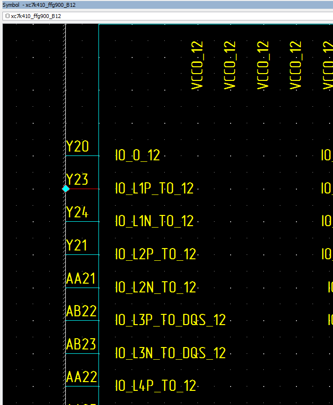
From the observations I can note that the latest names for Xilinx (for families of the 6th and 7th series) are quite meek and informative.
IO_L6N_T0_VREF_13
IO - I / O pin
L6N - designation of a differential pair
T0 - byte designation inside which you can swap data signals for memory (this point needs to be clarified!)
VREF - an external reference voltage can be supplied here if the standard of the selected signal for the bank requires it and there is no possibility to connect it inside the FPGA.
13 - bank number.
Altera also sometimes comes across normal functional designations, but more often (my subjective opinion) difficult-to-reproduce contact names, which then do not fit on the sheet with the scheme. Perhaps, if I made circuits with large amounts of memory, multipliers, or some colliders, I would need such a name.
IO_DIFFIO_T18p__DATA15_DQ3T0_X9__DQ3T9_X18_DQ5T27_X36
In this case, it helps to specify a Custom Label for the contact name. And enter the necessary name with your hands. I usually copy the functionality and reduce it to the form
IO_T18p_DATA15_DQ
In this case
IO - can be used for I / O signals
T18p is the number of the differential pair in the upper segment.
DATA15 - this contact can be used for parallel loading of the configuration.
DQ - tells me that this is an abbreviation of the functional purpose of the contact (there may still be DM and DQS)
This is one example of how a contact can be called on the basis of its functionality and for any particular project, some other sign will be displayed in the first place.
So, for example, with Altera, when using LVDS signals, you need to use an external load. For some banks, this is a load resistor only on the receiving side, and for others it is also needed at the output. This can be noted on the schematic symbol in the Custom Label property. The same applies to PCI signals type. Not all banks can be assigned standard bus 3.3V-PCI. And this can also be noted on the symbol. Despite the ever-increasing displacement of its standard PCIe in desktop systems, in the industrial performance, it is still popular. And some customers are looking for devices in this version.
You can add an inscription in the symbol for all contacts at once. This will reduce the amount of text inside the symbol. Since any additional information will overload the symbol and scheme, a compromise is needed here. I did this for Xilinx microcircuits, which have microcircuits that are compatible with the contacts inside one case with a different number of logic elements, but some of the contacts are not involved in the “small” microchips. Then, in the project, a part of the circuit was not soldered and it was possible to put a more “light” chip. Given this in the distribution of contacts, then you can save on the missing components and the price of the FPGA.
For convenience, I make banks-split characters. An exception can be made for contact configuration. If the project has a complex synchronization structure, then the CLK inputs — local, global, and others — can be assembled into a separate symbol. The power contacts of the VCCO banks are placed on the symbol with the bank or on a separate one - at the request of the PRIME developer.
Contacts power core, VCCAUX, land and other things, most often, stand on separate characters.
Allegedly, it is now possible for all power contacts to create only a circuit in the circuit and not to overload the circuit with a large number of contacts of the same type. We have not done so, so I am not familiar with such options. This can be found in the reference documentation or from webinars and online training materials on the site of Mentor Graphics and its representatives.
I transmit the created symbols directly to the design of the circuit, indicate the type of the enclosure, annotate the board and the chip is attached to the board, the circuit and the IODesigner.
Creating and assigning signals
As described above, we can export signals from a file or create them ourselves.
Signals can be assigned either by mouse or via import / export. By pressing the SHIFT, CTRL or ALT keys you can reassign signals to already assigned contacts. Or assign all selected signals to one bank. Visually, banks are displayed in different colors. Contacts of different types are displayed with different icons. You can enable the display of differential pairs. Over time, busy signals will be painted over.
We update the scheme and see the symbols on the diagram already with signals.
See how they are connected on the board. This is usually already shown above “porridge”.
Sometimes I immediately make a simple list of signals so that they are automatically created in the system, then I drag them to the circuit editor to other elements.
There is an option to import the list of signals from the scheme.
By synchronizing the design of the scheme, the board and the IO Designer, we can trigger the display of signals in the IO Designer window. With reaching chains from FPGA to the components connected to it.
Now we can comb our signals. And all this will be done automatically in accordance with the rules introduced by us. Configuration signals will not go anywhere. We can also pre-fix the signals to prevent a change in their location.
Please note that the DRAM3_RESET_B signal, to which the input / output standard LVCMOS_1.35V must be assigned and it cannot be located in the same bank with SSTL standard signals, is assigned to bank 17, and all other DRAM3 * signals to bank 12. As in the system Since only four signals with LVCMOS_1.35V, they are assigned the standard LVCMOS1.8V and supplied with a level converter.
Despite the seeming confusion of the signals, they are now straightened out in accordance with the rules assigned. For the convenience of working with the project in Quartus.
The image shows the placed components, and the lines drawn to them from the FPGA. Sometimes, if not all components are placed, it is impossible to expand all contacts for the first time without a trace. Although it all depends on the task.
After such a distribution of contacts, it is already possible to return the circuit to the final trace, or to trace it yourself.
You can also export to Verilog / VHDL file. We can export to * .ucf, * .pin or another file. To give it to the FPGA designer for a trial project, suddenly something was not taken into account. But in a small team it is not always possible to do this right away due to the heavy workload of other projects. (Old improvements, new wishes of customers or parallel projects).
Limitations.
This method has limitations, which I do not always know how to get around. But basically they are connected with the need to do a lot of things for versatility and in reserve. We have to invent crutches and stuff. So with Altera, by default, the differential signal should not be located near the differential signal. The compiler will issue a warning. We can bypass it by setting the parameter SLEW_RATE = 0 MHz in Pin Planner Quartus. After which the compilation will complete successfully. Even if in fact we have the signal will hang with a frequency of 20 MHz. There is no such parameter in IODesigner. As a result, on the diagram, these contacts are used by the latter or I set the type of signal to them so that it does not cause a conflict, for example, a PCB signal or a configuration one.
There are other limitations that are usually bypassed. But in general, I have a positive attitude towards them, since they force me to once again look into the documentation on the microcircuit much earlier than the ready payment arrives.
For those who work in other design systems, some things may not seem obvious and perhaps not necessary. So, as far as I know (heard), Altium allows you to customize the compilation of the project for the FPGA right in the project with the circuit and the board. I am not aware of all its capabilities. And for people who design it, they do not need import into Quartus or ISE. But we have a project of the printed circuit board is made by one person, projects for the FPGA by other people. When I give the circuit for tracing, I try to describe the signals as correctly as possible, while giving the PCB designer some freedom of action to change the contacts. We agree on any warnings that occur as they accumulate.
Finally, I would like to say that “IO Designer” is not a panacea. It does not turn the design of the circuit, board and project on the FPGA into an interactive game and does not exempt from studying the documentation on the chip. But working with such a tool is much more pleasant. The article does not describe all of its benefits. Also, I can not judge the completeness of libraries for all chips, since I only had to work with some of the Altera and Hilinx families. C Lattice I somehow managed to work a little bit on the debugging kit, but it didn’t get to the scheme, and even less to the board. With Actel, I did not work at all. From the comments on Xilinx, I can note that in my version there is no direct transfer of the file restrictions to / from Vivado. Maybe with the updates will be released. But since I am not leading the FPGA Xilinx project, I didn’t understand exactly what the problem was. We managed export through a * .csv file.
This publication does not claim to be a textbook on “IODesigner”, for this there are many lessons from Mentor Graphics. I know that in Russian the training is conducted by the company Megratek. www.megratec.ru .
Also, as far as I know, Mentor Graphics is preparing to introduce to the market xPedition - a new version of the design system. What is there to add specifically on IODesigner ʻu time will tell. Of those presentations that I saw, I was impressed by the update of the 3D display in the boards and the design of devices with several boards in one project.
Also, besides the CADs I mentioned, there are others for printed circuit boards. Each one has a list of advantages and a list of “what in Y is lacking as in X”. And if I did not name their advantages in comparison with the option of working through IOD - do not be offended. You can write about it in the comments. Or an article about how you design FPGAs in your CAD system.
Source: https://habr.com/ru/post/242531/
All Articles