SSP-based 1-Wire interface implementations
How to make steam out of the stone, our doctor Gaspar knows
Very often, when choosing a MC, one has to pay attention to the presence in its composition of a specific set of peripheral devices for a specific task. Meanwhile, a number of standard tires can be revised on the basis of other interfaces found in the already used MK. In this post, I will show how the 1-Wire hardware interface based on the existing SSP interface can be implemented on the MK 1986EV1T, and this experience can be transferred to other MCs from other manufacturers of a similar architecture.
To begin with a brief description of the microcontroller used. MK 1986EV1T produced by Milandr is a very good device, the merits of which are completely limited by the fact that these are domestic products (although for the author it was this parameter that was decisive). Indeed, a MC with a Cortex-M1 core with a clock frequency of up to 140 MHz is an infrequent market participant, and given the presence of a large number of different interfaces, an extended temperature range, and a version with a VP, then this MC becomes an almost unique proposition. However, it is necessary to note a number of properties that reduce the attractiveness of this MC for widespread use, namely: the high price determined primarily by the ceramic-metal case (although the developer announced a relatively cheap version in a plastic case), a rather inconvenient ceramic-metal case to use This type of corps allows for achieving an “honest” military temperature range), and (in the author’s opinion) an insufficient level of study of documentation (the problem of all domestic development Otok, which nevertheless does not justify).
I will give the main characteristics of this MK:
CORTEX-M1 core (with minor restrictions);
the clock frequency is up to 144 MHz (for frequencies above 25 MHz, delays are introduced when reading the program memory, which reduces the real speed to the equivalent 100 MHz);
')
program memory - 128 Kb, data memory - 48 Kb;
Both types of memory are easily expanded through the built-in 32-bit external system bus controller (which requires a significant number of external outputs);
developed clocking system with two internal generators (not too accurate), the ability to connect external quartz resonators and built-in PLL;
non-volatile memory (12 * 4 bytes) and a real-time clock (with external battery power);
8 * 12 bits ADC, 2 * 12 bits D / A, 8 timers with PWM mode;
32 channel PDP;
and a rich set of peripherals themselves - 2 * CAN, GOST 18977, 2 * GOST R-52070, Ethernet 10/100 (with integrated PHY!), USB Host / Device, 2 * UART (with integrated IRDA), 3 * SSP;
up to 96 user configurable legs;
possibility of programming and debugging from under common programming environments (the author prefers IAR) via SWD and JTAG.
In general, the crystal is quite decent, for more information, see the manufacturer's website. Of the shortcomings of the equipment, the author would have noted an undeveloped apparatus for interrupting external events (external interruptions can only come to a small number of predetermined conclusions), which limits the developer’s capabilities.
Another “hero” of this article is the 1-Wire interface. The interface is not standardized, it is the property of Dallas Semiconductor, it is known quite widely, it is used to interact with low-speed devices, among which the i-Button identification keys and different types of thermal sensors are particularly well known, the bus topology is a star with individual addressing, the exchange rate is up to 15 Kbd, the number of wires - 2, a more detailed specification is available on the website of the company. Many microcontrollers have a hardware implementation of this interface, however, the considered MK is not one of those. Therefore, we consider the possibilities of implementing the interface using standard MK 986BE1T peripherals.
First of all, we need to implement layer 1 of the OSI model - the physical interface. From this point of view, the interface is quite simple - an earthen wire and 1 wire are required, through which two-way interaction of devices is carried out and power is optionally transferred to the terminal device. To implement the information wire, an MK output with an open collector and a pull-up resistor of 5 Kom are required. All pins used MK configurable and can be equipped with built-in pull-up and down resistors (for more information, see the description of MK). The values of the built-in resistors differ from those required (according to rumors, they are about 10 Kom - according to rumors, since no data are given in the documentation), however, for the case with one source of information, it is possible to use built-in resistors, if necessary, it is easy to add an external resistor connected appropriate nutrition. Among the valid configurations of the MK pins, there is an open-drain output mode, which satisfies the interface requirements. Thus, the fundamental impossibility of the physical implementation of the interface was not found.
In the interaction of the master device (and we implement it) with the slave, an active zero level is applied, supplied in the form of pulses of various durations. 3 main pulse durations are used, namely:
a reset pulse with a duration of at least 480 microseconds, a transmission pulse of a unit with a duration of 1 to 15 microseconds (the same pulse is used to synchronize the reading), a transmission pulse of a zero with a duration of 15 to 60 microseconds. The guard interval between pulses must be at least 1 µsec, the pulse duration with a guard interval must be from 60 to 120 µsec. It should be noted here that if the requirements of the minimum duration are clear from the point of view of ignoring interference, then the limitations of the bit intervals from above are not so obvious and are not dictated by the logic of operation of the devices. Nevertheless, the restrictions are clearly spelled out and, accordingly, must be respected. When a slave device interacts with a master, 2 types of pulses are used, namely: a presence impulse in the form of a zero in response to a reset pulse with a delay relative to the termination of the latter from 15 to 60 microseconds and a duration from 60 to 240 microseconds, and a zero transmission pulse outputted in response a read pulse with a delay relative to the beginning of the latter is no more than 1 microsec and a duration of 15 to 60 microseconds (the interface documentation establishes a requirement of EXACTLY 15 microseconds with a subsequent delay for removing the pulse from 0 to 45 microsec - strange ato once wrote). General conclusion from the above - for the implementation of the 1-Wire interface, it is necessary to withstand time intervals with an accuracy of about 10 microseconds with top and bottom restrictions.
An obvious implementation of this protocol can be based on direct control of an output port configured in open source mode and connected by a pull-up resistor. For example, the implementation of a reset pulse with presence pulse control can be represented by the following pseudo code:
( 0), 500 , ( 1), 15 : 0 – - (), 45 : 0 – :: - ( ), :: 60 : 1- - ( ), 180 : 1- :: - ( ), :: - . In fact, even this procedure should be more difficult to eliminate the influence of impulse noise, but for the purposes of this article some simplifications are permissible.
Similar procedures can be implemented for the remaining pulses. Now consider the disadvantages of this option:
the lack of software implementation of delays - the dependence of the received time interval on the clock frequency MK and the execution time of individual commands and in the conditions of the introduction of delays in reading the program memory, the latter become almost uncertain),
and even if we overcame the first drawback with fine settings, then in terms of functioning together with other modules within RTOS or with interruptions (and they will almost always be, we are writing a non-spherical program in vacuum), the resulting time intervals can be much longer (but no shorter) than expected.
Since the interface is very time-dependent and the required accuracy is significant - 10 microseconds is not so much even on fast MKs, with high probability we will get chaotic failures when trying to communicate with devices via the 1-Wire bus. Although higher-level protocols can detect such failures due to redundancy of coding, it is not possible to recommend such a method of implementation. To combat such errors, it is necessary within critical sections (and in the above algorithm, all operations) to prohibit interruptions and block the ability to switch tasks for a sufficiently long time, which is not a good programming style.
A variant of this implementation can be the use of one of the general-purpose timers or the system timer to form the necessary time slots. If we take into account the delay in overhead costs, we can fairly accurately maintain the time diagram and eliminate the first drawback of the above implementation. Nevertheless, the second drawback is fundamentally unavoidable within the framework of the decision, since in all RTOS (or in the presence of interrupts) it is possible to guarantee only that the ordered event will not occur before the specified time, but that restrictions from above are impossible.
So, for the implementation of the 1-Wire interface, we need the ability to issue time-tightly limited top and bottom intervals and the ability to monitor the state of the MK pins at precisely defined time intervals. Such a possibility exists for MC with advanced timers (including hardware state machines), but this MC is not one of them. It is also possible to use hardware-implemented serial interfaces, which we will do. The MK implements many serial interfaces, however, not all of them can be used for our purposes. For example, the USB interface operates at a fixed frequency and its hardware is rigidly tied to the protocol, so it is hardly possible to modify it so significantly for our purposes, as is also the case for CAN and GOST. The situation with C UART is much better, its speed can be varied over a wide range, and the presence of a start bit is not an obstacle, since any impulse starts from an active level, and the presence of a stop bit can be taken into account when calculating time parameters. The only significant limitation is the mismatch of active levels, which can be eliminated by the introduction of a matching element. But, since all 2 UARTs were busy for other tasks, this solution was not worked out.
As a result, it was decided to implement the 1-Wire interface based on one of the three universal modules of synchronous serial communication SSP. A detailed description of the capabilities of these modules can be found in the documentation of the manufacturer MK. In short, these modules allow synchronizing with the module clock frequency generated inside the MC to output information to the output port with a serial code and simultaneously receive information on the input port of the MC with reference to the above frequency. At the same time, we will use the output and input of the module data connected together, but we don’t use signals on the clocking and synchronization lines and we can use them as general-purpose lines, which is allowed by the flexible configuration system of MC pins. It is assumed to use the transmitted byte to encode the time intervals associated with the transmission / reception of one bit, while the values of the byte bits determine the duration of the active level (bit 0) and its absence (bit 1). When determining the SSP settings, it should be taken into account that the minimum transmission interval should be from 1 to 15 microseconds, and the maximum counting interval is from 60 to 120 microseconds for information bits and at least 480 for the reset signal. If you select 10 microseconds as the minimum interval, then the first condition is satisfied, and the bit interval will be 6-12 minimum intervals, and the figure 8 fits well into this range. Then the duration of the reset signal will be at least 48 clock cycles, which exceeds the number of bits in a byte. To solve the latter question, one should either change the duration of the minimum interval, or use more than 1 byte of information to transmit a pulse. The latter method could create a problem with the uncertainty of the intervals between transmissions of individual bytes of the parcel and, accordingly, the duration of the resulting pulse could increase unpredictably. Fortunately, the SSP module is equipped with a FIFO buffer of 8 16-bit words, so that the total buffer length of 16 * 8 = 128 bits overlaps the required minimum possible sequence length of 480 + 60 + 240 = 780/10 = 78 bits.
Thus, the following algorithm works with the SSP: we set up the required mode and the required transmission frequency, prohibit the transmitter operation, fill the transmitter buffer with information to issue the required time intervals, enable the transmitter operation. The module starts transmitting information by a serial code along the output data line, at the end of the transmission a ready flag is set, which serves as a signal that the next piece of data can be generated. In this case, the timing diagram of the transmitted signal is rigidly tied to the clock frequency of the module, which depends only on the clock frequency of the MC and can not be in any way changed, no matter what programs are running at that moment. In this case, between transmission of individual bytes of the sequence can only be intervals determined by the equipment, which can be taken into account when forming the sequence (studies have shown that such intervals can be eliminated). Consider the process of setting up an SSP module.
The SSP module can operate in three modes -
Motorola SPI;
Texas Instruments SSI;
Microwire interface from National Semiconductor.
Of these three modes, the latter is not suitable, since it imposes additional requirements on the signal format, the first two look equivalent, before we start exploring them on an oscilloscope. Here it turns out that the SPI mode is characterized by delays of 1 bit between the transfer of neighboring words, which serves to transmit a synchronization signal, which we do not use. This would not be so important, since it would slightly increase the inter-bit intervals if 0 did not appear on the data line at these moments, which is completely unacceptable according to the requirements of 1-Wire.
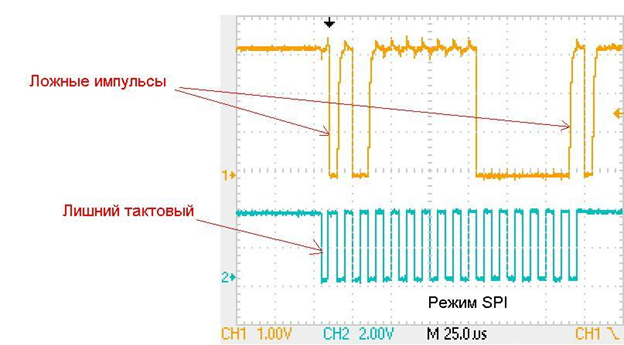
Figure 1. False Pulses in SPI Mode
It is very fortunate that the SSI mode is devoid of such a disadvantage, otherwise it would have had to significantly complicate the program. Studies have shown that in the SSI mode, inter-word intervals are simply absent (the synchronization pulse is transmitted during the last bit) and, accordingly, there are no gaps on the transmission line. It should be noted that at the time of configuration, undocumented changes in signal levels are observed on the transmission and synchronization lines, but they do not affect this implementation, since working with the device after setting up the SSP module still begins with a reset pulse, which will suppress any consequences of these emissions.

Figure 2. False impulses at the time of switching on SSI
Since the problem was solved in an easy way, they did not look for the cause of the emissions, although for applications that use the current SSI mode, they would have to understand. In the above oscillograms, the following reference signal was applied, corresponding to the pattern 0xBF81.
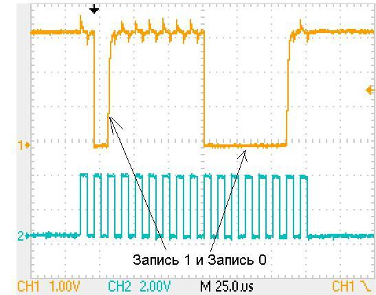
Figure 3. A signal without false pulses.
In all figures, the upper signal (yellow) is the data line, the lower signal (blue) in Fig. 1 and 3 is the clock frequency line, in Fig. 2, the synchronization line. The lower signal in the implementation of the interface is not used and is given in the reference order for determining the time intervals.
Thus, the transmission of a reset pulse and the control of the presence of a presence pulse can be represented by the following pseudo-code:
; 0F800 00000 00000 001FF 0xFFFF 0xFFFF // (50 , 500 , 410 ); ; " "; ; 6 – – SSP; 0xF800 0x0000 0x0000 0b000X1XXXXX0XXXXX 0xXXXX 0xFFFF – – - . Let me clarify some points - the transfer to SSP goes simultaneously with the reception, and the moment of gating the input data is shifted by half the clock (at our clock frequency of 5 microseconds), so when reading you should get exactly the same number of words as transmitted, and when transferring zeros accepted zero, except for the last (here should be 1, but the specific value depends on the capacity of the line and the resistance of the pull-up resistor). The next feature is that the “buffer is empty” flag is set immediately after the last word of information is transferred to the shift register, but until the transfer of bits is completed, therefore, the device free flag should be used (see technical documentation), otherwise we will not see the last received word. Further, you can use different patterns to obtain more detailed information about the faults of the device, but this is the subtleties of the technical implementation.
For the transmission of zero and one pulses, similar procedures are easily created, and it is logical to transmit 2 bits of 1-Wire in a row in one 16-bit word SSP. The recommended procedure is to send immediately a 1-Wire byte in 4 words SSP. At the end of the transfer, you should not forget to read the receiving buffer in order to remove from there a copy of the transmitted data. For reading, you should form a sequence corresponding to record 1, and analyze the received information to extract the value of the received bit (we pass the pattern 0b01111111, we take 0b01111111 in case of 1 or 0b00XXXX11 in case of 0). To transfer long messages, you can (and this has been implemented) consider the option of organizing software using an advanced direct memory access (again, not well documented), one of the channels of which is responsible for interacting with the SSP module.
It should be noted that the proposed organization of the interface has a drawback - the received values are fixed along the front of the clock signal, that is, we can “catch” short pulses on the line that will distort the received information. This problem can be solved by a more detailed analysis of the received information, for example, in the received pattern 0b00100111, the third left single bit should be considered an interference. Of course, such a method cannot be considered optimal, although it must be understood that the probability of such an event is disproportionately less than the probability of failure under the option of a purely software implementation. However, in the used MK 1986EV1T there is an opportunity to deal with interference at the hardware level, namely, each input port is equipped with a plug-in Schmidt trigger to increase noise immunity and, moreover, is equipped with a plug-in filter that suppresses short pulses at the inputs. Unfortunately, like many other interesting decisions of the microcontroller developers, this part is very poorly documented.
On the basis of the above techniques, a library of subroutines in the C language is implemented for working with the 1-Wire interface through the 1986B1T microcontroller SSP module of the following composition:
1. The bottom layer of the work with the hardware is the subprograms for managing the registers MK, which are part of the BSP MDR1986VE1T, available on the manufacturer's website.
2. The next layer includes low-level write and read functions that are not public.
3. The interface implementation layer provides the developer with full access to the 1-Wire interface and includes the following modules:
Init1Wire - initializes the hardware of the requested SSP module and returns a pointer to the control structure;
Reset1Wire - performs the initial installation of connected devices and reports on their presence;
Search1Wire - searches for devices connected to the interface and returns their addresses;
Adres1Wire - addresses a specific device on the interface;
WriteByte1Wire - writes a random byte to the selected device;
ReadByte1wire - reads 1 byte from the selected device.
4. In the interface implementation layer, additional functions were created to simplify interaction with the device:
WriteData1Wire - writes a dataset to the selected device;
ReadData1Wire - reads the dataset from the selected device.
5. The device implementation layer is built on the basis of layer 3 and is presented as an example of interaction with an electronic key of the DS1990 type.
The general conclusion is that the MK 1986EV1T is an interesting product of a domestic manufacturer with the possibility of creating various digital devices on its basis and presents to the trained specialist rich possibilities for implementing various interfaces, including non-standard microcontrollers, with minimal software costs.
PS If the post is interesting to the public, then in the following I could describe the implementation all on the same I2C SSP interface.
Source: https://habr.com/ru/post/239981/
All Articles