Autonomous SDR receiver on FPGA
Earlier, I already wrote about a homemade SDR receiver , made on the basis of the DE0-nano debug board. Like most other SDR receivers, it was not able to work without being connected to a computer. At the same time, a large number of unused resources remained in the used FPGA, so I decided to make the receiver completely autonomous.
How the whole SDR receiver works, and how to implement it - next.
A little about the previous project
The task of any receiver is to amplify the signal from the antenna, select the desired high-frequency signal, transfer it to low frequencies (most often sound), and demodulate the resulting signal. A difficult problem here is precisely the selection of a certain high-frequency signal from the entire radio. Usually, the desired signal is located relatively in a narrow frequency band (most radio amateur signals are less than 4 kHz wide), and other radio signals are located next to it, the reception of which will only interfere. Therefore, analog radio amateur receivers are quite complex, they have to do several frequency conversions, and install fairly complex band-pass filters. The presence of various methods of modulation of signals also requires the receiver to introduce a set of demodulators.
With the spread of powerful computing technology, it became possible to transfer part of the receiver’s functionality to a computer. Due to digital signal processing, it is possible to create very efficient bandpass filters (albeit low-frequency ones), demodulate signals of any type, display the spectrum of the received signal.
')
In most modern receivers, the transfer of a signal from a higher frequency to a lower one is done by mixing (multiplying) the original signal with a signal from the reference oscillator - the local oscillator. As a result, a signal appears at the mixer output with a frequency equal to the frequency difference between the original signal and the local oscillator.

However, in this case, signals that are both lower and higher than the local oscillator frequency (frequencies A and B in the figure) can be received. This phenomenon is called the “mirror channel”. To combat it, analog receivers share filters and transfer to intermediate frequencies.
There is another method of suppressing a mirror channel - phase, using quadrature signal mixing ( method description ). The peculiarity of this method is that for its implementation in a receiver it is necessary to realize two phase shifters of a sufficiently high order, and their characteristics must be identical, which requires an accurate selection of components and complicates the design of the receiver and its setup.
Since in digital form several different signals can be processed in exactly the same way, it is possible to create fairly simple but effective receivers. In such receivers, the signal after the quadrature mixer is filtered out of the RF signals, amplified, digitized by the ADC and transmitted to a computer or DSP. This technology is used in most SDR receivers.
Block diagram of such a receiver:

With the availability of a suitable high-speed ADC and FPGA, even quadrature conversion and decimation of the resulting signal can be performed in digital form. Receivers of this type are called DDC (Digital Down Conversion). Due to the fact that in this receiver there are practically no analog components, it is possible to obtain a very high attenuation factor of the “mirror channel”.
This is the receiver I described earlier. It included an external ADC, and signal multipliers implemented in the FPGA, a digital signal generator, CIC and FIR filters, as well as modules for transmitting the received information to a computer. The receiver transmitted 16 bit x 50 ksps x 2 channels via Ethernet.
And now it is worth going to the description of an SDR receiver capable of operating autonomously.
Signal extraction and demodulation
Earlier in my receiver these operations were performed by a computer. Now it was required to implement them on the FPGA.
Block diagram of the resulting demodulator:

Since we wanted to be able to change the frequency of the received signal without changing the basic frequency of the receiver tincture, it was necessary to add an additional generator and an integrated multiplier to the demodulator unit. The generator (NCO1) forms a sine wave and a cosine wave, and can be tuned in the range of 0-25 kHz.
To transfer the desired signal to the area of zero frequencies, a quadrature multiplier is used. An important feature of his work is that due to the fact that complex signals are multiplied together, no mirror channel appears at its output.
There is also a module that allows you to swap tires connecting the NCO1 and a multiplier, thereby changing the direction of the signal shift (this module is not shown in the diagram).
The result of the transfer of signals:

However, the above frequency transfer does not solve the problem of the mirror channel.
The phase of the signals at the output of the quadrature mixer depends on their position relative to the frequency of the local oscillator: those above this frequency will have a phase difference in channels I and Q +90 degrees, below -90 degrees.
Thus, if you additionally shift all signals in channel I by +90 degrees, then the phase difference of the signals will be already either 180 or 0 degrees. It is enough to add the resulting signals to each other, and the unwanted mirror channel will be suppressed (adding signals with a phase difference of 180 degrees gives zero). If instead of adding, we subtract signals, then the mirror channel will be received - in this way you can switch the type of the received band: LSB / USB.
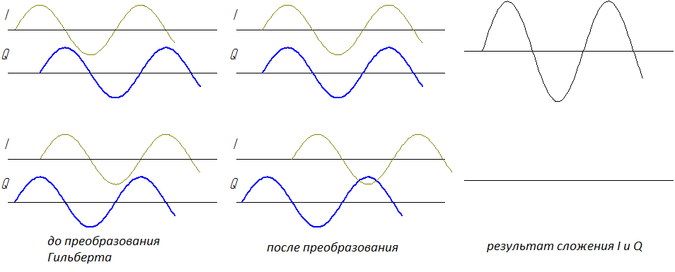
To perform the phase shift in the demodulator module, a digital phase-shifting filter ( Hilbert Transform ) is introduced. It performs the phase shift of all frequency components of the signal by 90 degrees.
The filter was calculated using the FDATool tool included in Matlab. In fact, the Hubert filter is simply a kind of FIR filter with certain coefficients. FDATool even allows you to generate a VHDL code for the resulting filter. The order of the filter used is 65.
A feature of the Hilbert filter is that at frequencies of 0 and Fs / 2, its transmittance tends to 0. In this case, this means that frequencies in the LF range from 0 to ~ 500 Hz will not be accepted.
The Hilbert filter delays the signal by N / 2 samples, where N is the order of the filter. To compensate for this effect, a delay line (FIFO buffer) is introduced into the Q channel, delaying the signal by 34 samples.
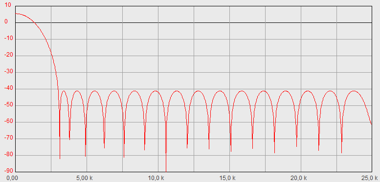
After the signals of the I and Q channels are folded, the resulting signal must be filtered, passing the signals in the 0-3 kHz band to the output. This is done to facilitate the reception of SSB signals, which usually have such a band. I note that if several radio stations operating as telegraph fall into this band, all of them will be heard.
The filter uses a ready-made FIR filter from Quartus. It has an order of 32, the coefficients for it, were also calculated in FDATool.
The frequency response of the resulting filter:
All demodulator modules are 12 bits wide. A smaller bit would give a not very high-quality sound, a big one would require more FPGA resources, which were clearly not enough. The clock frequency for all modules is 50 kHz (data rate at the output of the decimation filters).
Sound output
In order to output the audio signal from the FPGA, I used a PWM driver. This is not the best way to create a sound signal, but the simplest one. The clock frequency of the PWM driver is high enough - 100 MHz. With such a frequency with a bit width of 12 bits, the frequency of the PWM pulses is 24 kHz.
Since the received signals have a very large dynamic range, then for normal reception, we had to introduce software automatic gain control (AGC) into the design. It is implemented quite simply - if the amplitude of the signal at the output of the demodulator is too large, the AGC module attenuates the signal at the input of the demodulator (the Right Shifter block inside it is used for this purpose). The signal is attenuated 2 ^ N times due to a simple shift, which is not very convenient, but it is implemented very simply by software and practically does not require FPGA resources. If within 0.2 seconds the signal at the output of the demodulator is low, then the attenuation of the signal decreases. The disadvantage of this method is that the switching of the gain is sometimes quite well heard.
FFT, spectrum display and receiver control
Earlier I already implemented work with a VGA monitor on a DE0-nano. I also experimented with the FFT module .
Thus, it was enough to transfer the available modules to the receiver project, and connect the outputs of the decimation filters to the FFT module input - and it became possible to observe the spectrum of the radio signal in the + -25 kHz band from the main oscillator frequency - NCO2. The sound demodulator and FFT work independently, so you can change the frequency of the received signal without changing the receiver tuning frequency.
The FFT module - ready from Quartus, 512 points long, works in conjunction with the window function module.
Traditionally, the spectrum is displayed using its logarithmic representation. However, it seemed to me not very informative, in addition, the module of the hardware calculation of the logarithm occupied too many FPGA resources, and the calculation of the logarithm went out software too long. So the value of the amplitude of the spectrum before output to the screen is simply reduced by 2 ^ N times, the number N can be changed programmatically.
In this project, data capture from the FFT module, data output to the VGA screen, operation with SDRAM, receiver control is performed using the SOPC system, which includes the NIOS II software processor.
Simplified SOPC block diagram:

To control the receiver, I decided to use a PS / 2 mouse. It is quite simple , the whole connection goes through two wires. On the Altera website, among the examples for some debugging boards, a module for SOPC, designed to work with PS / 2, was explicitly mentioned. I came across the code (I can’t specify the links, because I couldn’t find the needed ones again). The found example had to be changed to work with my system frequency, but at first it still did not work. The situation was complicated by the fact that the PS / 2 bus is bidirectional, with a five-volt bus, and the FPGA runs from 3.3V. As it turned out, in order for the mouse to work properly, you need to supply 5V to it (at 3.3V, the mouse does not start), in the Quartus settings, the pins used for PS / 2 should be specified as working from 3.3V (the other pins are set to 2.5 C). Also, for reliable operation, we had to install a 470pF capacitor between the CLK line and the ground. Perhaps, if an external voltage converter is used, problems could be avoided.
Then I managed to establish a connection with the mouse from Nios, but even then there was a problem - I could not adjust the frequency of data output by the mouse. As it turned out later, this was the problem of a particular type of mouse. Working with the mouse at the program level is not difficult - after initialization, when moving, it sends 3 bytes to the FPGA, which the mouse controller receives at the SOPC. It also generates an interrupt for Nios, in which handler Nios calculates the new coordinates of the cursor.
The interface, implemented at Nios, allows you to observe the spectrum, the "waterfall", to control the receiver setup (main local oscillator), adjust the frequency of sound reception, the type of received band - USB / LSB. The tuning frequency can be changed by clicking on the corresponding digit on the frequency indicator with the left / right mouse button (similarly, the frequency can be changed in many computer SDR programs). The frequency of tuning the sound reception can be changed by clicking with the mouse to the right place on the spectrum or “waterfall”.
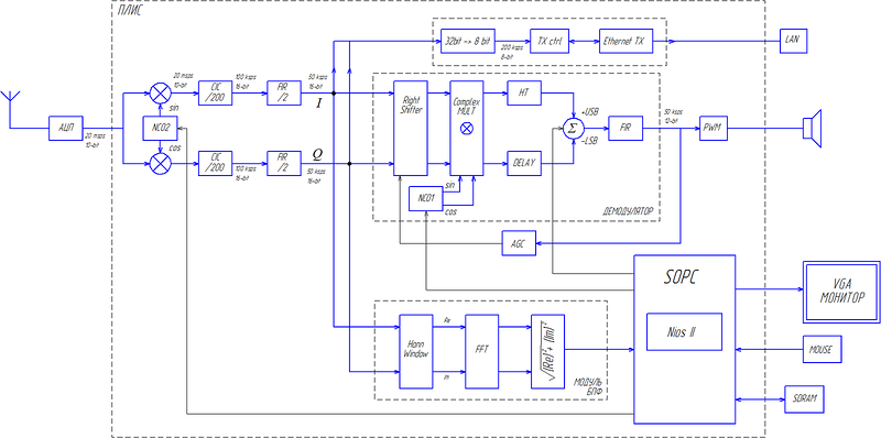
Block diagram of the entire receiver:
Quartus layout
FPGA resources used by the project
As I wrote above, in the process of creating a project, certain difficulties arose related to the scope of the project. It uses a large number of filters that take up space both in logical elements (LE) and use hardware multipliers. When setting the parameters of each block, one had to choose which filter length to use. Due to the lack of resources, some filters had to be switched to the symmetric mode, which reduces the number of multipliers used by the filter. Nevertheless, the parameters of the Hilbert filter and the FIR filter in the demodulator are quite mediocre (in computer programs, they are much more efficient). It is worth noting that in the resulting design, the FPGA resources are not fully used - the clock frequency of most modules is 50 kHz, although they can operate at a much higher frequency.
Also, a lot of resources are occupied by SOPC with Nios - more than 6000 LE.
In total, the project uses:
LE: 21.445 / 22.320 (96%)
9-bit multipliers: 98/132 (74%)
As you can see, almost all LE FPGAs are used.
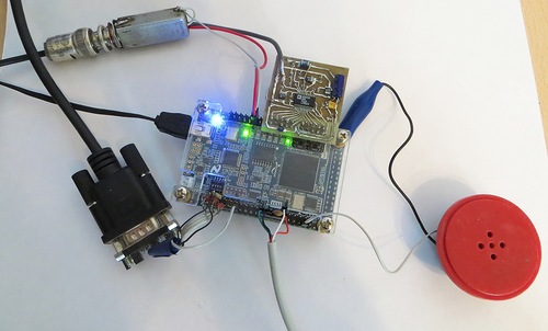
General view of the receiver:

Close-up:
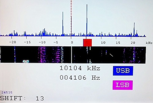
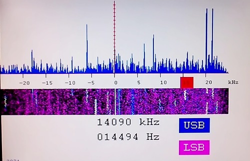
Screen during operation (during CQ WW RTTY DX Contest):
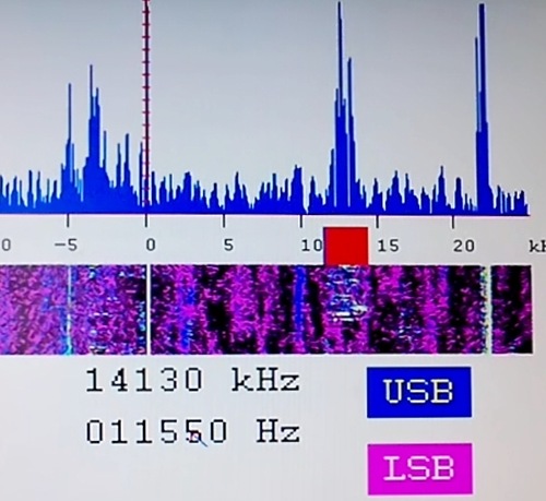
SSB reception:
Video of the receiver:
From the video you can judge the quality of the receiver. It is worth noting that at the hearing the sound is somewhat better than on the phone recording on video. Also, as I mentioned earlier in the previous post, the antenna is not the best used.
At the receiver, it was possible to receive rtty signals (connected to the PDA receiver, they were decoded), JT65 signals were received (they were decoded on a computer). The German radio station broadcasting the meteofax was well heard.
Link to the project
Source: https://habr.com/ru/post/237859/
All Articles