Confused FPGA technology
While working on the next game (training) FPGA project for the Mars Rover 2 board, I was faced with the fact that I clearly do not have enough space in the crystal. It seems the project is not very complicated, but my implementation is such that it requires a lot of logic. In principle, this is nonsense, something everyday. Well, if you really need, you can choose a FPGA with a larger capacity. Actually, my project is the game “Life”, but implemented in FPGA in the Verilog HDL language .
About the logic of the game, I will not tell, about her, and so it has already been written enough .
')
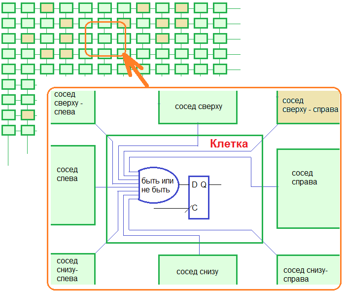
The idea of the project is this: every cell in the playing field is a separate calculator. Each computer has its own logical function and its own register, which stores the current state of the cell (live / not live). All space for the life of cells is a two-dimensional array of calculators, calculators form a whole network. All computers work synchronously, since a single clock frequency is applied to all registers. The figure above should clarify the project outline.
So here. On my motherboard is Altera's Cyclone III EP3C10E144C8 FPGA. 10 thousand logical elements. At first I thought I could make a two-dimensional array of cells 128x64 = 8192 cells. Does not fit. 64x64 = 4096 - the same does not fit in the crystal. How so. I managed to fit only 32x16 = 512 cells in the FPGA. Pichalka ...
Reflections lead me to believe that it is possible, in the future, the FPGA technology will grow into something more than programmable logic. Here I would like to tell you about this vision. To a sophisticated reader I will say straight away that much further written is merely a figment of the imagination and may even be nonsense.
But..
At present, the FPGA technology is used by a rather narrow circle of specialists. Basically, FPGAs are used for prototyping chips and for small-scale products, when manufacturing ASIC chips is not economically viable. FPGA specialists, I think, not very much. The technology is quite complex and requires many specific knowledge. On the other hand, for the organization of high-speed and parallel computing of the FPGA is perhaps the most suitable technology.
We know, for example, that Altera offers and promotes OpenCL technology.
Simply put, this is such a C-like language for describing parallel computing in an FPGA accelerator. By the way, Nvidia and its video cards also support parallel computations with OpenCL .
Thus, it is clear that Altera is clearly thinking about how to bring "ordinary" C-like parallel FPGA computations to the people. Let's see what's up with the prices for parallel computing with FPGA? Terasic DE5-Net.
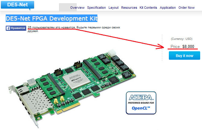
25 users like the price of 8 thousand bucks (just kidding).
There are other attempts to bring the FPGA to the people - Altera has released together with Intel the E6x5C series chip , where the Atom processor and the Arria II FPGA are connected in a single package. Good try, but the technology seems so and could not find a mass consumer.
Apparently existing FPGA crystals do not fit into the modern programming paradigm.
And what is the current modern paradigm of "normal" programming?
It seems to me that something like this:
- the computer always runs several computational processes and threads simultaneously
- the state of processes and threads is stored in memory, the process can request the OS as much memory as needed; you can even ask for more than there is physical memory - and the process can actually get this virtual memory.
- calculations are made by the processor, sometimes it has many cores. Usually, a process or thread does not know (or does not want to know) in which core of the processor the task is being performed.
- a higher priority may displace a lower priority. To force out is to save the state of the memory pages of the sluggish process to disk and switch to a higher priority process. Give him more time slice.
It is clear that the more memory and the more processor cores, the faster all the processes in the system work.
Memory and processor cores are computer resources, computers, which the operating system distributes between processes.
Now let us imagine that in the future we will get computers, where along with the memory and processor cores there will still be “like-plis” logic blocks. This resource "as it were-plis" in its properties is located somewhere between the processor and memory. On the one hand, “as it were, plis” = this is a calculator, that is, closer to the processor, but on the other hand, it is also memory, because there is quite a lot of information stored in the registers. The state of the calculator "as it were-plis" is already quite difficult to save in the task_struct structure when the task context is switched. But, probably, you can try to supplant the state of the logic blocks in the swap file, like virtual memory. And the OS can temporarily load other logic blocks for the active thread ...
By the way, both Altera and Xilinx have for a long time already had an FPGA with the possibility of partial reloading of individual sections, blocks of logic ( Partial Reconfiguration ) - that is, in principle, they somehow go in this direction ...
The programmer can allocate as much as-plis for the process as needed. Literally function lalloc (logic alloc) by analogy with malloc (memory alloc). Then from the file to read there "FPGA firmware" and it will live and work. We, programmers, by and large do not have to think about whether this system has a memory / logic “like-a-play” or not. And not our business. Yes, sometimes it can be very slow with limited resources, but don't we know how video games “lag” on weak video cards? Users know that they will have to pay for strong iron, but it would be good if even the minimal system already had logic-as-plis blocks for use in programs in the basic version.
In fact, of course, I imagine that such a technology is unlikely to appear soon, it is all too complicated and not realizable. At least the existing FPGA chips are not suitable for this purpose, if only because slow serial JTAG interfaces are used to configure the FPGA. But maybe sometime one of us will do this?
PS: by the way, here’s my life game in FPGA, so small, 32x16 ... well, I don’t have a virtual
2: all the sources and a detailed description of the project of the game Life can be found here .
Source: https://habr.com/ru/post/236161/
All Articles