Raise SOC: ARM + FPGA
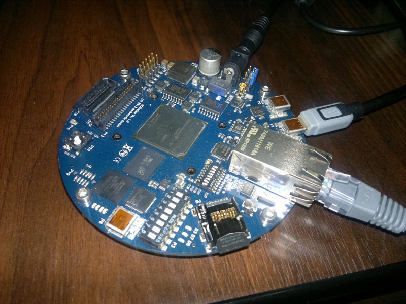
The other day, the EBV SoCrates Evaluation Board came into my hands. In a nutshell - this is a board with SoC from the company Altera , on board which there is a dual-core ARM and FPGA Cyclone V.
ARM and FPGA on the same chip - it should be very interesting! But first, all this good must be “raised”.
I will tell about this process in this article.
')
If you get into the hands of such or a similar board and you are not completely sure what to do with it. If you always thought that FPGA is something complicated and it is not clear how to approach this. Or you are just a curious engineer. Then come in. We are all happy.
And as a small bonus, let's measure the bandwidth between the CPU and the FPGA .
Work plan
Our plan consists of the following points:
- Getting FPGA Firmware
- Kernel build
- Build U-Boot and Preloader
- Build rootfs
- Writing test programs
- Create SD card
- Startup and bandwidth measurement
Go!
Creating FPGA Firmware
First of all we need to get the FPGA firmware.
From the tools for this you need a Quartus CAD, you can download it on the official website
I will not describe the installation - everything is pretty obvious there.
Project creation
Run Quartus, go to File -> New Project Wizard , click Next , fill in the directory and the name of the project:
Project name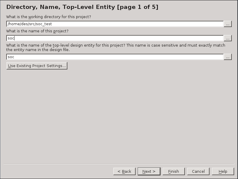
The next page is skipped, then there is a choice of family and type of FPGA.
FPGA selection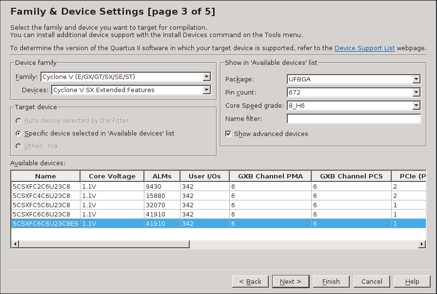
The remaining settings are not important for us, click Finish .
Qsys project
Qsys is a great tool for beginners. Allows you to get the firmware without writing a single line of code. Instead, the developer assembles a constructor from predefined cubes (IP peels). You only need to properly adjust each crust and connect them properly.
So, Tools -> Qsys , in the left window ( IP Catalog ) we will need two IP peels:
- Processors and Peripherals -> Hard Processor Systems -> Arria V / Cyclone V Hard Processor System
- Basic Functions -> On Chip Memory -> On Chip Memory (RAM or ROM)
Hard Processor System (HPS) is our ARM. With its settings and begin.
On the first tab, we are interested in HPS-to-FPGA interface width , so that we have access from the CPU to the internal memory of the FPGA:
FPGA Interfaces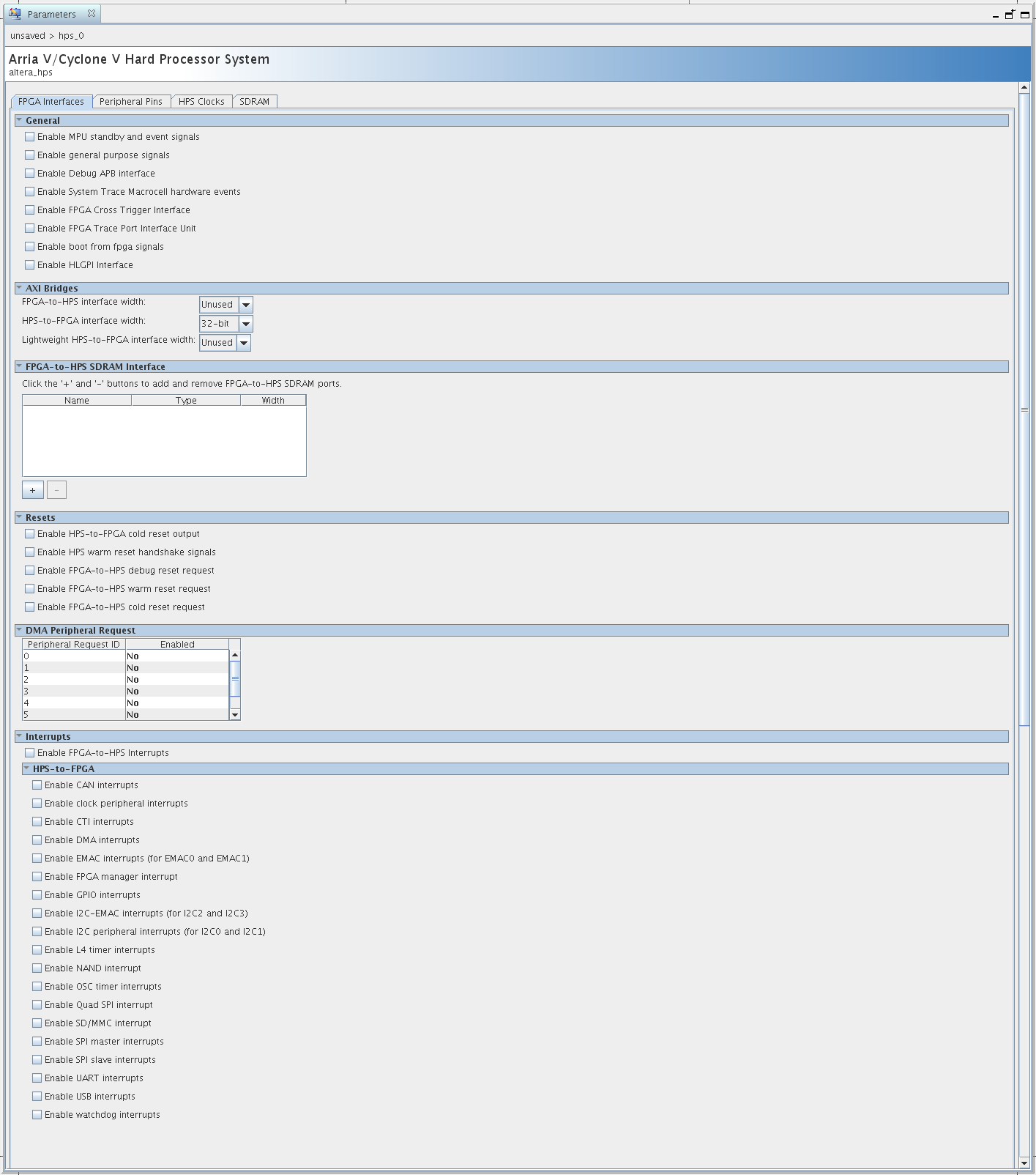
Next comes a bunch of settings for various interfaces - in which modes work, which pins are used:
Peripheral pins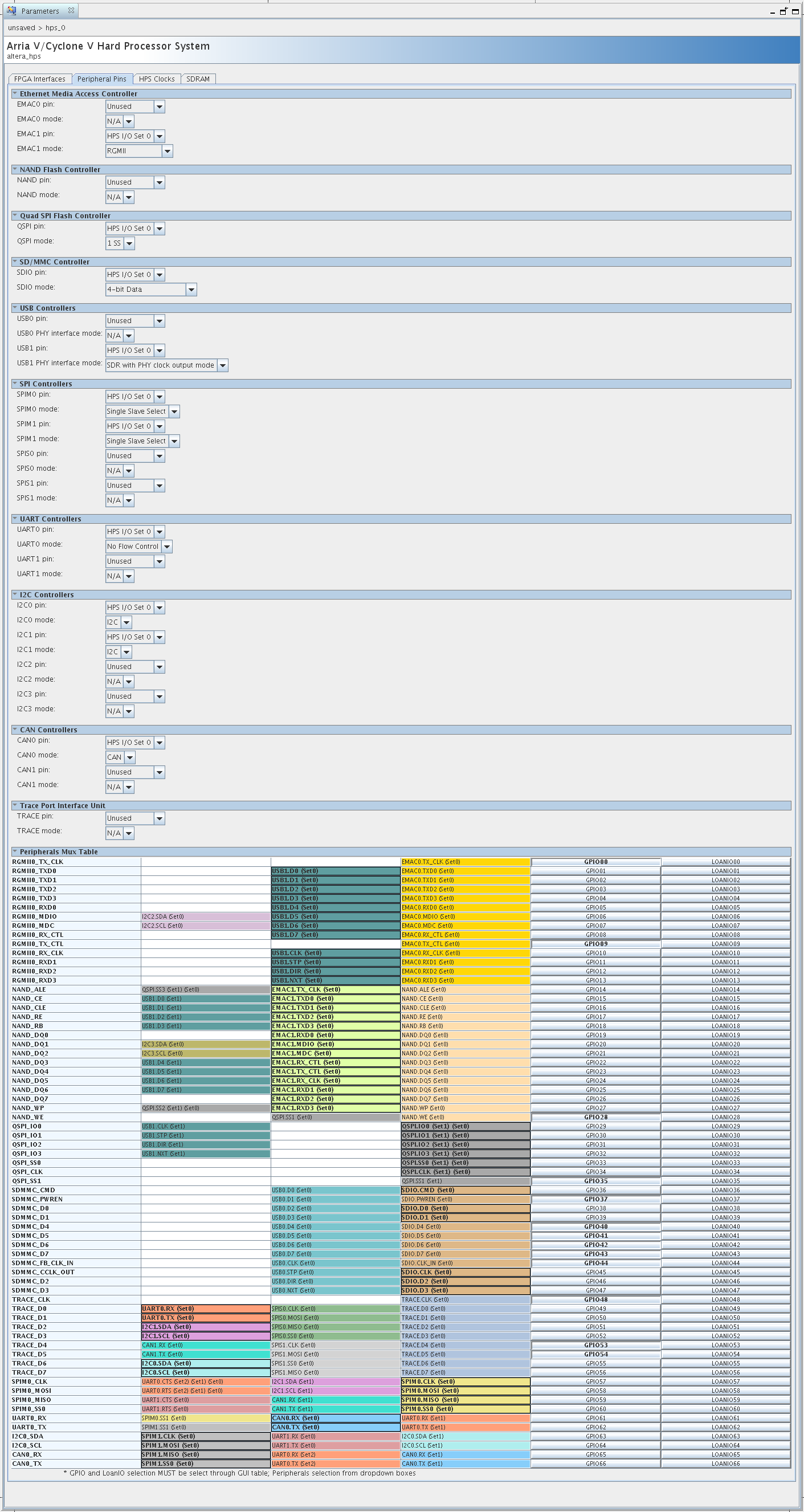
The next tab is setting up clocks. In Inputs Clocks leave everything unchanged:
Input clocks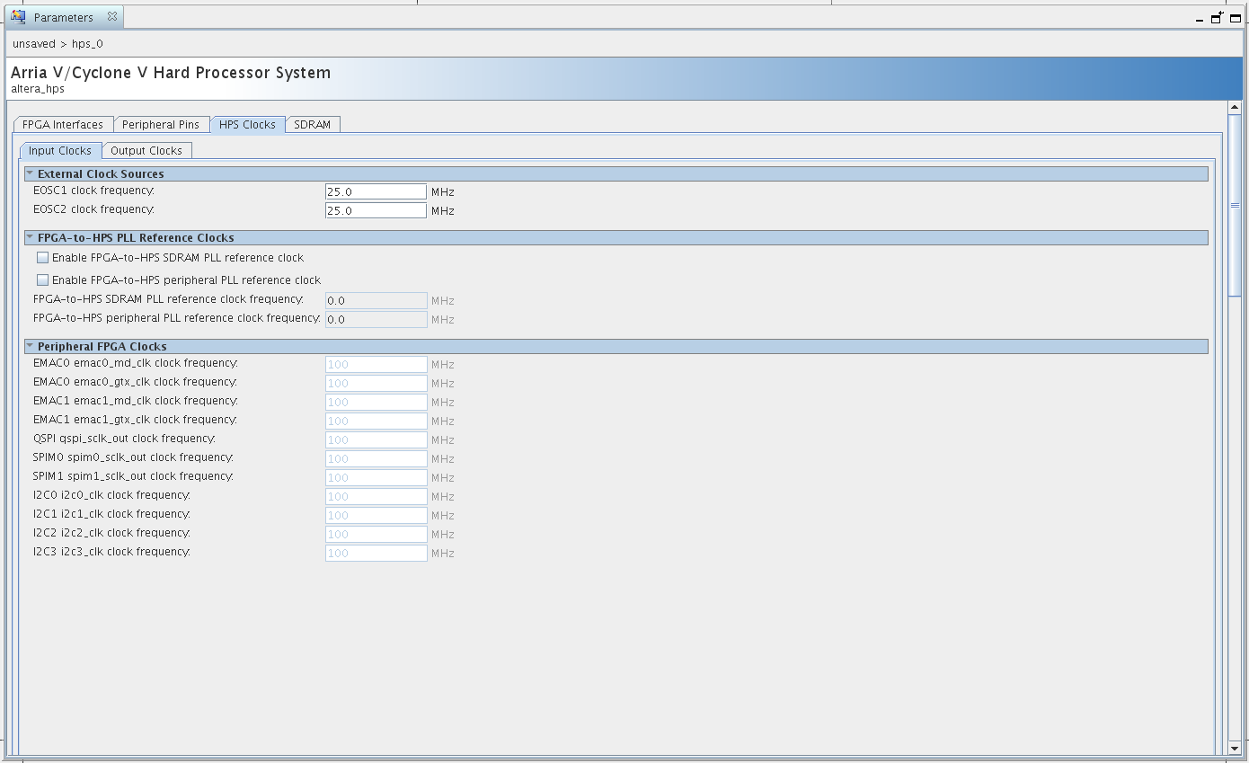
In the Output Clocks set the checkbox to Enable HPS-to-FPGA user 0 clock :
Output clocks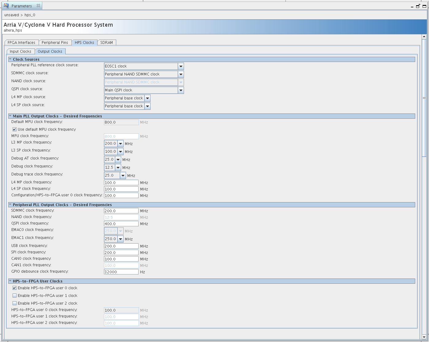
Then there is a large subsection with different settings for DDR3 memory.
DDR3 PHY Setting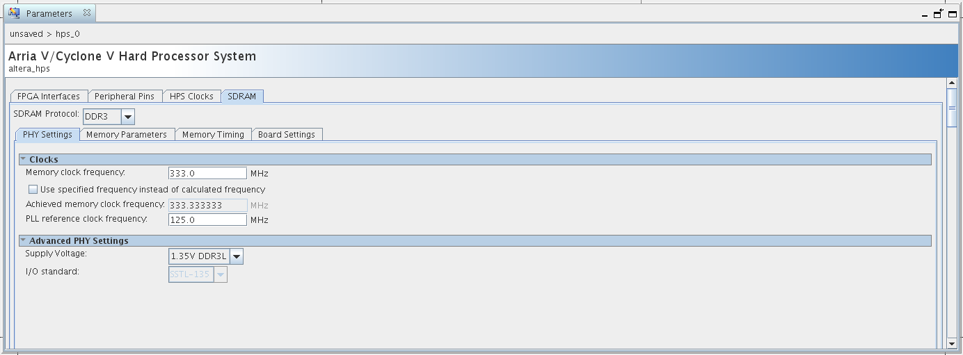
DDR3 Memory Parameters
DDR3 Memory Timing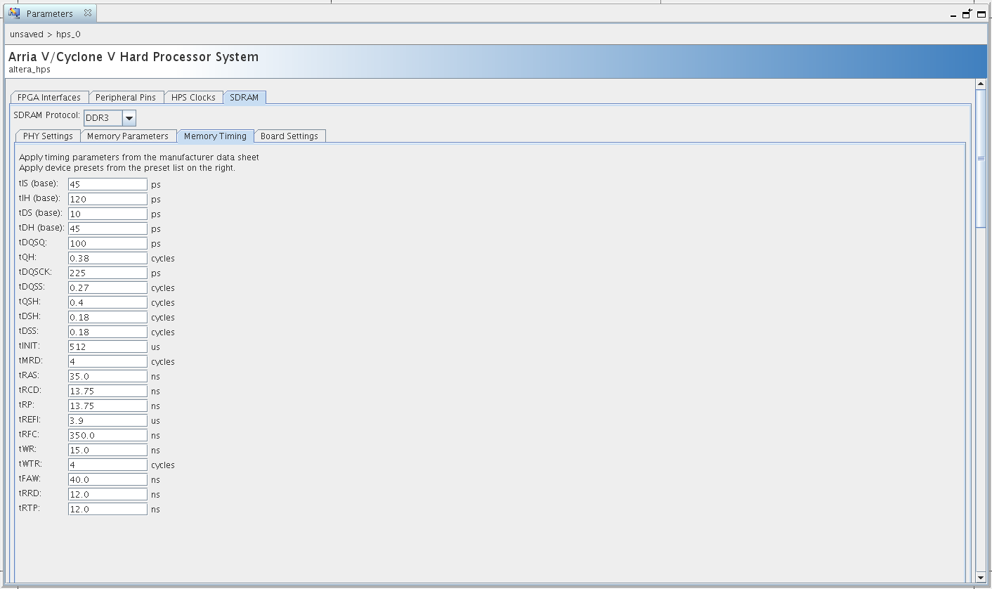
DDR3 Board Settings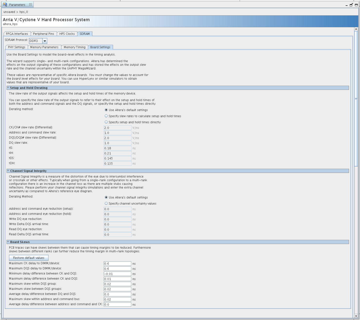
With HPS we figured out, go to the setting of On-Chip memory. This is a memory that is located directly inside the FPGA.
There are significantly fewer settings:
On-Chip Memory
Now you need to connect the blocks together. Everything is quite intuitive (note the value of the base address opposite s1 ):
Qsys Connections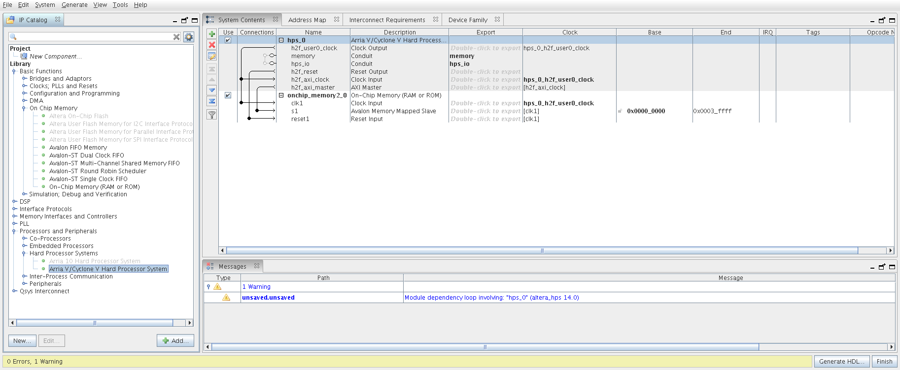
Is done. Save ( File -> Save ) under the name soc.
It remains to generate files. Generate HDL button, in the appeared window again press Generate , wait, Finish .
Project compilation
Now you need to add the generated files to the project:
Assignments -> Settings tab Files , add the file soc / synthesis / soc.qip
It is necessary to apply the settings for DDR pins. But before that you need to perform the first stage of compilation:
Processing -> Start -> Start Analysis & Synthesis
Run the script to configure the pins:
Tools -> Tcl Scripts . In the window that appears, select Project -> soc -> synthesis -> submodules -> hps_sdram_p0_pin_assignments.tcl , Run .
Final project compilation:
Processing -> Start Compilation
We received the file soc.sof with FPGA firmware. But we want to flash the FPGA directly from the CPU, so we will need a different format. Perform the conversion. This can be done from the GUI, but in the console easier. And indeed, it’s time to break the GUI off :).
To convert, you need to start the terminal and go to the directory with our project. Then go to output_files and execute the command (do not forget that the directory with Quartus utilities must be in the PATH variable):
quartus_cpf -c soc.sof soc.rbf Hooray! We got the FPGA firmware.
Kernel build
Now we will assemble the core for our ARM.
From tools you will need Altera SoC EDS . From here we will take the arm-linux-gnueabihf- compiler for cross-compiling.
We pump out the core:
git clone https://github.com/coliby/terasic_MTL.git Run the script that will add the compiler directories to the PATH and launch bash :
/opt/altera/quartus14.0/embedded/embedded_command_shell.sh Set the environment variables:
export ARCH=arm export CROSS_COMPILE=arm-linux-gnueabihf- export LOADADDR=0x8000 Go to the directory with the kernel and perform the configuration:
cd terasic_MTL/ make socfpga_defconfig Build a kernel image for U-Boot :
make -j 4 uImage Now we need to get the so-called .dtb (Device Tree Blob) file. This is a binary file containing information about the platform - interfaces, pins, clock signals, address space, etc. The kernel reads this file during initialization and makes changes to it. This allows you to use one assembled core on multiple hardware platforms.
So, we get the .dtb file:
make socfpga_cyclone5.dtb But this file is not for our platform, so we will have to make small changes to it. To do this, convert the file to text format .dts (Device Tree Source):
./scripts/dtc/dtc -I dtb -O dts -o soc.dts arch/arm/boot/dts/socfpga_cyclone5.dtb Now in soc.dts you need to remove the block bridge @ 0xff200000 . This can be done either by hand or by applying a patch:
patch soc.dts dts.patch dts.patch
942,966d941 < bridge@0xff200000 { < compatible = "altr,h2f_lw_bridge-1.0", "simple-bus"; < reg = <0xff200000 0x200000>; < #address-cells = <0x1>; < #size-cells = <0x1>; < ranges = <0x200 0xff200200 0x80 0x100 0xff200100 0x80>; < < tsc@0x200 { < compatible = "terasic,mlt_touch_screen"; < reg = <0x200 0x80>; < width_pixel = <0x320>; < height_pixel = <0x1e0>; < interrupts = <0x0 0x28 0x4>; < }; < < vip2@0x100 { < compatible = "ALTR,vip-frame-reader-13.0", "ALTR,vip-frame-reader-9.1"; < reg = <0x100 0x80>; < max-width = <0x320>; < max-height = <0x1e0>; < mem-word-width = <0x100>; < bits-per-color = <0x8>; < }; < }; < Now convert the file back to .dtb :
./scripts/dtc/dtc -I dts -O dtb -o soc.dtb soc.dts So, we are interested in two files:
- arch / arm / boot / uImage
- soc.dtb
Build U-Boot and Preloader
The process of starting the SoC is as follows:
- Boot rom
- Preloader
- Bootloader
- OS
Boot ROM - this is the first stage of the boot, which is performed immediately after raising the power. Its main function is to define and execute the second stage, Preloader .
Preloader functions are most often the initialization of the SDRAM interface and the configuration of the HPS pins. The initialization of SDRAM allows the next stage to be loaded from external memory, since its code may not fit into 60 KB of available internal memory.
Bootloader can participate in the further initialization of HPS . This stage also loads the operating system or user application. Usually (and in our case) U-Boot acts as a bootloader .
OS - everything is simple. This is our favorite Linux . We already have a kernel for it, we will get the root file system a bit later.
And now we will deal with Preloader and U-Boot
Open the terminal, run the script already familiar to us:
/opt/altera/quartus14.0/embedded/embedded_command_shell.sh Go to the directory with our project:
cd ~/src/soc_test/ After compilation, the hps_isw_handoff directory should appear there , go to it:
cd hps_isw_handoff We start the generation of the necessary files:
bsp-create-settings --type spl --bsp-dir build --preloader-settings-dir soc_hps_0 --settings build/settings.bsp --set spl.boot.WATCHDOG_ENABLE false After this, the build directory should appear.
Putting Preloader:
make -C build Putting up the U-boot:
make -C build uboot Now we need to set up variables for U-Boot . First, create a text file u-boot-env.txt .
u-boot-env.txt
console=ttyS0 baudrate=115200 bootfile=uImage bootdir=boot bootcmd=run mmcboot bootdelay=3 fdt_file=soc.dtb fdt_addr_r=0xf00000 ethaddr=00:01:02:03:04:05 kernel_addr_r=0x10000000 mmcroot=/dev/mmcblk0p2 mmcpart=2 con_args=setenv bootargs ${bootargs} console=${console},${baudrate} misc_args=setenv bootargs ${bootargs} uio_pdrv_genirq.of_id=generic-uio mmc_args=setenv bootargs ${bootargs} root=${mmcroot} rw rootwait mmcboot=mmc rescan; ext2load mmc 0:${mmcpart} ${kernel_addr_r} ${bootdir}/${bootfile}; ext2load mmc 0:${mmcpart} ${fdt_addr_r} ${bootdir}/${fdt_file}; run mmc_args con_args misc_args; bootm ${kernel_addr_r} - ${fdt_addr_r} verify=n Then we convert it into a binary format, not forgetting to specify the size of the region containing the variables - 4096 bytes is enough for us. Even if the actual size exceeds the specified, mkenvimage will report this.
./build/uboot-socfpga/tools/mkenvimage -s 4096 -o u-boot-env.img u-boot-env.txt We are interested in three files:
- build / uboot-socfpga / u-boot.img
- u-boot-env.img
- build / preloader-mkpimage.bin
Build rootfs
This section is written for those who use Debian (or if your distribution also has debootstrap ). If you are not among them, you can use Yocto or any other method convenient for you.
Install the necessary packages:
sudo apt-get install debootstrap qemu-user-static binfmt-support Create a directory and download the necessary files there:
mkdir rootfs sudo debootstrap --arch armel --foreign wheezy rootfs http://ftp.debian.org/debian To run applications compiled under the ARM architecture, we will use qemu static . To do this, copy the file to our rootfs :
sudo cp /usr/bin/qemu-arm-static rootfs/usr/bin/ Go to our new file system:
sudo chroot rootfs /bin/bash If the interpreter's invitation has changed to “I have no name! @Hostname: / #”, then everything went well.
Finish the installation process:
/debootstrap/debootstrap --second-stage In / etc / inittab we leave the following lines:
/ etc / inittab
id:5:initdefault: si::sysinit:/etc/init.d/rcS ~~:S:wait:/sbin/sulogin l0:0:wait:/etc/init.d/rc 0 l1:1:wait:/etc/init.d/rc 1 l2:2:wait:/etc/init.d/rc 2 l3:3:wait:/etc/init.d/rc 3 l4:4:wait:/etc/init.d/rc 4 l5:5:wait:/etc/init.d/rc 5 l6:6:wait:/etc/init.d/rc 6 z6:6:respawn:/sbin/sulogin S:2345:respawn:/sbin/getty 115200 console Set password:
passwd Create an archive:
tar -cpzf rootfs.tar.gz --exclude=rootfs.tar.gz / Writing test programs
In a nutshell, almost all interaction between SoC components occurs by mapping the address space of one component into the address space of another.
Consider an example. In our project with the help of Qsys, we indicated that on the HPS-to-FPGA interface, starting from address 0, there is an On-Chip memory block with a size of 262,144 bytes. The HPS-to-FPGA interface itself is mapped to the CPU address space at 0xC0000000 (see the documentation for Cyclone V ). As a result, CPU access by addresses from ( 0xC0000000 + 0 ) to ( 0xC0000000 + 262143 ) will result in accessing the internal FPGA memory.
Therefore, to work, we need a utility with which you can read / write about arbitrary memory addresses. Here is its source code:
mem.c
#include <stdio.h> #include <stdlib.h> #include <stdint.h> #include <fcntl.h> #include <sys/types.h> #include <sys/mman.h> #include <unistd.h> #include <errno.h> #define MAP_SIZE (4096) #define MAP_MASK (MAP_SIZE-1) int main( int argc, char *argv[] ) { int fd; if( argc < 2 ) { printf( "Usage:\n" ); printf( "%s byte_addr [write_data]\n", argv[ 0 ] ); exit( -1 ); } // /dev/mem , . fd = open( "/dev/mem", O_RDWR | O_SYNC ); if( fd < 0 ) { perror( "open" ); exit( -1 ); } void *map_page_addr, *map_byte_addr; off_t byte_addr; byte_addr = strtoul( argv[ 1 ], NULL, 0 ); // /dev/mem . . map_page_addr = mmap( 0, MAP_SIZE, PROT_READ | PROT_WRITE, MAP_SHARED, fd, byte_addr & ~MAP_MASK ); if( map_page_addr == MAP_FAILED ) { perror( "mmap" ); exit( -1 ); } // ( ) map_byte_addr = map_page_addr + (byte_addr & MAP_MASK); uint32_t data; // , , -- . if( argc > 2 ) { data = strtoul( argv[ 2 ], NULL, 0 ); *( ( uint32_t *) map_byte_addr ) = data; } else { data = *( ( uint32_t *) map_byte_addr ); printf( "data = 0x%08x\n", data ); } // . if( munmap( map_page_addr, MAP_SIZE ) ) { perror( "munmap" ); exit( -1 ); } close( fd ); return 0; } Now you need to build it using the cross compiler. To do this, run the script:
/opt/altera/quartus14.0/embedded/embedded_command_shell.sh And compile:
arm-linux-gnueabihf-gcc -o mem.o mem.c We also need a bandwidth measurement utility:
memblock.c
#include <stdio.h> #include <stdlib.h> #include <stdint.h> #include <fcntl.h> #include <sys/types.h> #include <sys/mman.h> #include <unistd.h> #include <errno.h> // #define COP_WRITE (0) #define COP_READ (1) #define COP_CHECK (2) int main( int argc, char *argv[ 0 ] ) { int fd; void *map_addr; if( argc < 5 ) { printf( "Usage:\n" ); printf( "%s <cop> <address> <word_count> <cycles>\n", argv[ 0 ] ); exit( -1 ); } // /dev/mem , . fd = open( "/dev/mem", O_RDWR | O_SYNC ); if( fd < 0 ) { perror( "open" ); exit( -1 ); } uint8_t cop; off_t addr; uint32_t word_cnt; uint32_t cycle_cnt; // cop = strtoul( argv[ 1 ], NULL, 0 ); // addr = strtoul( argv[ 2 ], NULL, 0 ); // / word_cnt = strtoul( argv[ 3 ], NULL, 0 ); // cycle_cnt = strtoul( argv[ 4 ], NULL, 0 ); // /dev/mem . map_addr = mmap( 0, word_cnt * 4, PROT_READ | PROT_WRITE, MAP_SHARED, fd, addr ); if( map_addr == MAP_FAILED ) { perror( "map" ); exit( -1 ); } uint32_t cycle; uint32_t word; uint32_t data; // switch( cop ) { // "". case( COP_WRITE ): for( cycle = 0; cycle < cycle_cnt; cycle++ ) { for( word = 0; word < word_cnt; word++ ) { *( ( uint32_t *) map_addr + word ) = word; } } break; // . case( COP_READ ): for( cycle = 0; cycle < cycle_cnt; cycle++ ) { for( word = 0; word < word_cnt; word++ ) { data = *( ( uint32_t *) map_addr + word ); printf( "idx = 0x%x, data = 0x%08x\n", word, data ); } } break; // " ". case( COP_CHECK ): for( cycle = 0; cycle < cycle_cnt; cycle++ ) { for( word = 0; word < word_cnt; word++ ) { data = *( ( uint32_t *) map_addr + word ); if( data != word ) { printf( "Error! write = 0x%x, read = 0x%x\n", word, data ); exit( -1 ); } } } break; default: printf( "Error! Unknown COP\n" ); exit( -1 ); } if( munmap( map_addr, word_cnt * 4 ) ) { perror( "munmap" ); exit( -1 ); } close( fd ); return 0; } Compile:
arm-linux-gnueabihf-gcc -o memblock.o memclock.c Accordingly, the files of interest to us:
- mem.o
- memblock.o
Create SD card
It is time to put the pieces together. At the moment we should have the following files:
- soc.rbf
- uImage
- soc.dtb
- preloader-mkpimage.bin
- u-boot.img
- u-boot-env.img
- rootfs.tar.gz
- mem.o
- memblock.o
If there is no one of them, then you missed something :)
Create a directory and copy all the specified files into it. Next we need to find and connect the microSD card.
In subsequent commands, the card is assumed to be defined as a / dev / sdb device. We will create two sections on it:
- / dev / sdb1 - for Preloader and U-Boot
- / dev / sdb2 - for filesystem
If the map is defined under a different name, make the appropriate changes.
Just in case, we will overwrite everything with zeros.
Attention! Once again check that / dev / sdb is a card, not your second hard disk.
sudo dd if=/dev/zero of=/dev/sdb bs=10M In order to create partitions, use the fdisk utility:
sudo fdisk /dev/sdb Next, you need to enter the following commands (empty line - enter Enter):
Commands for fdisk
o n p 1 2048 +1M n p 2 t 1 a2 t 2 83 w You can check what we did:
sudo fdisk -l /dev/sdb It should be something like:
Fdisk -l output
Disk /dev/sdb: 1966 MB, 1966080000 bytes 61 heads, 62 sectors/track, 1015 cylinders, total 3840000 sectors Units = sectors of 1 * 512 = 512 bytes Sector size (logical/physical): 512 bytes / 512 bytes I/O size (minimum/optimal): 512 bytes / 512 bytes Disk identifier: 0x02be07e5 Device Boot Start End Blocks Id System /dev/sdb1 2048 4095 1024 a2 Unknown /dev/sdb2 4096 3839999 1917952 83 Linux Now copy the image with U-Boot variables to the map:
sudo dd if=u-boot-env.img of=/dev/sdb bs=1 seek=512 After this, copy the Preloader :
sudo dd if=preloader-mkpimage.bin of=/dev/sdb1 And the U-Boot itself :
sudo dd if=u-boot.img of=/dev/sdb1 bs=64k seek=4 Create an ext3 file system:
sudo mkfs.ext3 /dev/sdb2 Mount it:
sudo mount /dev/sdb2 /mnt/ And we deploy our rootfs into it:
sudo tar xvf rootfs.tar.gz -C /mnt/ Next, copy the kernel image, dtb , FPGA firmware and test programs:
sudo cp uImage /mnt/boot/ sudo cp soc.dtb /mnt/boot/ sudo cp soc.rbf /mnt/boot/ sudo cp mem.o /mnt/root/ sudo cp memblock.o /mnt/root/ Unmount the file system:
sudo umount /dev/sdb2 Everything, the map is ready!
Startup and bandwidth measurement
Finally, everything is ready for work. Insert the card, connect the USB and power.
Go to the console:
minicom -D /dev/ttyUSB0 -b 115200 -s First of all, FPGA .
For this it is necessary to set the switch P18 on the board to the “On On On On” position (switches 1 to 5).
We look at the current state of FPGA :
cat /sys/class/fpga/fpga0/status We should see the configuration phase
Fill the firmware:
dd if=/boot/soc.rbf of=/dev/fpga0 bs=4096 And look at the state again:
cat /sys/class/fpga/fpga0/status The state should change to user mode . This means that the FPGA is configured and ready for operation.
Now we check our utilities. But before that, a little more "work with a file."
Our cross-compiler and Debian have different dynamic linker names. Therefore, in order for the utilities to work, we need to create a link to the correct linker:
ln -s /lib/ld-linux.so.3 /lib/ld-linux-armhf.so.3 So, we run the utility (an explanation of what kind of address will be slightly lower):
./mem.o 0xFFD0501C If as a result you see the line data = 0x00000007 , then everything is in order.
As I wrote above, the internal memory of the FPGA will be mapped into the address space starting at address 0xC0000000 . But before we can work with this memory, we need to do two more actions.
The first is that since by default all interfaces between the CPU and the FPGA are in reset, we have to remove it. The block Reset Manager (rstmgr) , with the base address 0xFFD05000 , and specifically its register brgmodrst with offset 0x1C, are responsible for this. The final register address is 0xFFD0501C . Only three low-order bits are involved:
- 0th - reset of the HPS-to-FPGA interface
- 1st — LWHPS-to-FPGA interface reset
- 2nd — FPGA-to-HPS interface reset
The logic of all bits is the same - if there is a unit there, then the corresponding interface is in reset. As a result, the default value for this register is 0x7 , which we saw when we read from it with the help of our utility. We need to remove the reset from the HPS-to-FPGA interface, so we have to write the number 0x6 into the register:
./mem.o 0xFFD0501C 0x6 After this, we again read the register to make sure that the data were recorded correctly:
./mem.o 0xFFD0501C Secondly, we need to enable the mapping of the HPS-to-FPGA interface to the CPU address space. The unit L3 (NIC-301) GPV (l3regs) with the base address 0xFF800000 , and specifically its remap register with offset 0, is responsible for this. For HPS-to-FPGA responsible bit number 3 . As a result, we need to write the number 0x8 into the register:
./mem.o 0xFF800000 0x8 Unfortunately, this register is available only for writing, so we will not be able to read the data for verification.
Now we can read and write in FPGA memory. Check it out. We read:
./mem.o 0xC0000000 Naturally, there should be zeros. Now write something there:
./mem.o 0xC0000000 0x12345678 And read again:
./mem.o 0xC0000000 Must match the recorded.
Hooray! We finally made it! We got a working SoC with FPGA and organized access to its memory from the CPU .
But just reading / writing is somehow quite boring. Let's at least measure the bandwidth of our interface. Moreover, it will take very little time.
For this we need our second memblock utility:
root@desktop:~# ./memblock.o Usage: ./memblock.o <cop> <address> <word_count> <cycles> It works as follows: if the first cop argument is 0, then the word_count of 32-bit words, starting with the address address , will contain a sequence of numbers from 0 to word_count-1 . The entire procedure will be performed cycles times (this is done for more accurate measurement of the bandwidth).
If cop is 1, then the same words will be read and displayed.
If cop is 2, then the words will be read, and their meanings will be compared with those that were hypothetically recorded.
Check it out. Let's write some data:
./memblock.o 0 0xC0000000 10 1 Now we consider them:
./memblock.o 1 0xC0000000 10 1 The result should be as follows:
Output memblock.o
data = 0x00000000 data = 0x00000001 data = 0x00000002 data = 0x00000003 data = 0x00000004 data = 0x00000005 data = 0x00000006 data = 0x00000007 data = 0x00000008 data = 0x00000009 Now let's try to compare the data, specifically asking a little more words:
./memblock.o 2 0xC0000000 11 1 Should get the following string:
Error! write = 0xa, read = 0x0 Now we start recording over the entire memory capacity in the amount of 1000 repetitions and measure the recording time:
time ./memblock.o 0 0xC0000000 0x10000 1000 The average of 5 starts is 11.17 seconds. Consider the bandwidth:
1000 * 65536 * 4 * 8 /_ / ( 11.17 * 10^6 ) = 187.75 /c Not very thick. And what about reading?
time ./memblock.o 2 0xC0000000 0x10000 1000 Average time 10.5 seconds. What translates into:
1000 * 65536 * 4 * 8 / ( 10.5 * 10^6 ) = 199.73 /c About the same. Naturally, for the execution of any of these operations, one of the two cores is loaded at 100%.
If you add the -O3 flag during compilation, then the write and read bandwidth will be 212 Mbit / s and 228 Mbit / c, respectively. Slightly better, but also not a meteor.
But this is not surprising - we did not do anything to increase this bandwidth. It would be nice to play around with a more tricky optimization, look towards the core, or, at worst, at least screw DMA to unload the processor.
But this is already in the next article, if, of course, it will be interesting to someone.
Thanks to those who got to the end! Good luck!
useful links
Official Cyclone V Documentation
Rocketboards.org - many different articles about boards with SoC
Information specifically on the EBV SoCrates Evaluation Board
Source: https://habr.com/ru/post/235707/
All Articles