Place under the ... antenna
It often happens that the space for an antenna on a digital printed circuit board (PCB) is allocated according to the residual principle - the antenna is rigidly pushed onto the remaining free space. Yes, and the antenna is chosen "as it will", the main thing - to fit. In such a situation, it is not at all necessary to talk about any calculations or matching the antenna with the existing circuit. Why it is better not to do this, but to take the “antenna” task more seriously, it will be discussed below.
I think the most interesting is to consider the situation described above with a specific example. So, we have a designed printed circuit board of a device that communicates over the radio channel in the frequency range 2.4 ... 2.48 GHz. This board is exactly the case when the antenna was placed on the residual principle, since The main task was to minimize the dimensions of the printed circuit board. After the manufacture of prototypes of PP and their installation, it turned out that the range of the radio channel is much less than the calculated one. At the same time, there were no problems with the circuit design of the created software. The method of elimination came to the conclusion that the antenna could be the culprit of the current situation.
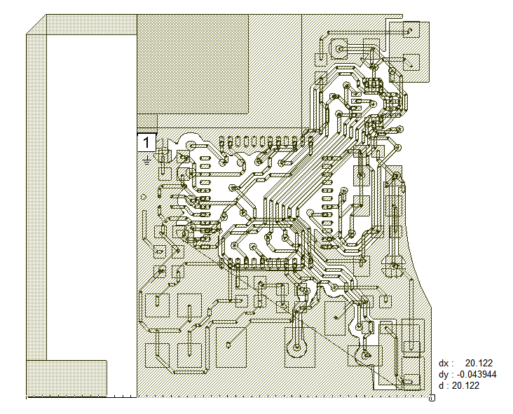
Due to the small dimensions of the PP (15 mm by 20 mm), it was impossible to put a coaxial-microstrip junction (CMP) on it to connect the antenna directly to the measuring equipment. Therefore, it was decided to evaluate the characteristics of the antenna using special CAD systems. Fortunately, we have such an opportunity at the department. So, Figure 1 shows a 3D view of a printed circuit board with layers that affect the antenna characteristics of a printed emitter.
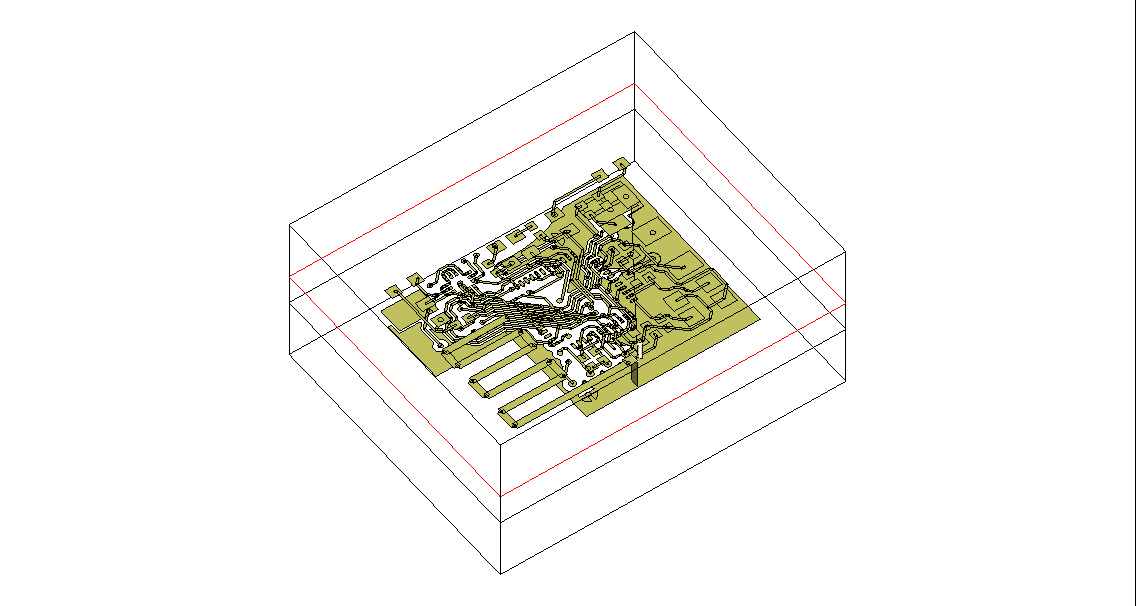
Fig. one
')
The number 1 denotes the area of inclusion of the device in the antenna.
And the following figures are the graphs of the characteristics of the antenna, calculated in the simulator. Let's look at a little more detailed graphics characteristics.
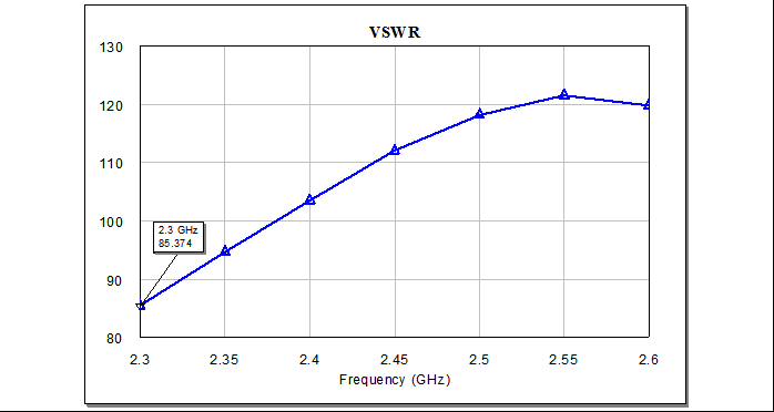
The VSWR schedule (Figure 2) allows to assess the degree of matching the antenna with the 50-ohm line (which, in fact, the signal is fed to the antenna). As can be seen from the graph, the minimum value of VSWR = 85 (and I would like the VSWR to be no more than 2).
Pic2
What does this mean? This suggests that 95% of all power supplied to the antenna is reflected back into the path. Thus, it is clear that the mismatched antenna radiates, at best, 5% of the input power, which leads to the fact that the range of the radio channel is significantly less than expected. Why it happens?
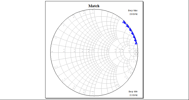
Figure 3 shows a graph of the complex impedances , from which it is clear that the antenna is inductance and its characteristic impedance is very far from 50 Ω.
Pic.3
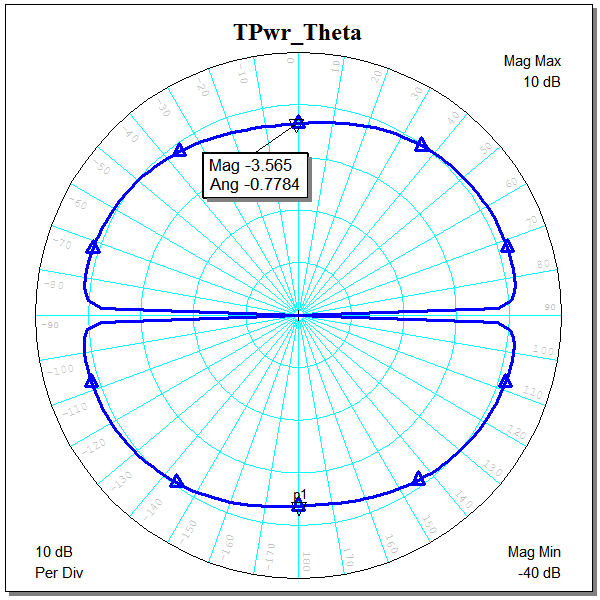
And finally, the graphs of the radiation pattern (NF) in elevation (Figure 4) and azimuth (Figure 5) planes. Solely so that later it was possible to compare different versions of the implementation of the antenna.
Pic.4

Pic.5
Well, the most important question - what to do? In terms of austerity space on the PP options a bit. The option was recognized as a worker when the PCB increases by no more than 5 mm along the narrow side (i.e., new board dimensions of 20 mm by 20 mm). In this situation, it was decided to use the printed monopole, as the most compact. Figure 6 shows the modified topology with a new antenna.
Pic.6
Now everything looks a little better ...
This is how the VSWR looks like:

Fig.7
Here is the impedance diagram (the previous version is shown in blue, the new version is pink):

Fig.8
And NAM:

Fig.9 DN in elevation plane

Fig.10 DN in the azimuthal plane
As you can see, the new version is much better than the previous one. Along the edges of the working range, the maximum VSWR = 2.7: the power loss is about 20%. Of course, this option is a compromise between the dimensions of the printed circuit board and the antenna parameters, but it is 100% working.
In addition, the result can be even better if you do not bend the antenna, and straighten it and run along the edge of the board. For example, to do this (see Figure 11) and in this embodiment, the antenna can be placed along the body of the device.

Figure 11
At the same time, the obtained characteristics will be better than the previous version and much better than the original version (for the last version of the antenna, the graphics are brown).

Fig.12
From the graph in Figure 12 it can be seen that the last version of the antenna has the best VSWR = 1.25. Those. power loss is less than 1.5%.

Fig.13

Fig.14 Nam in elevation plane
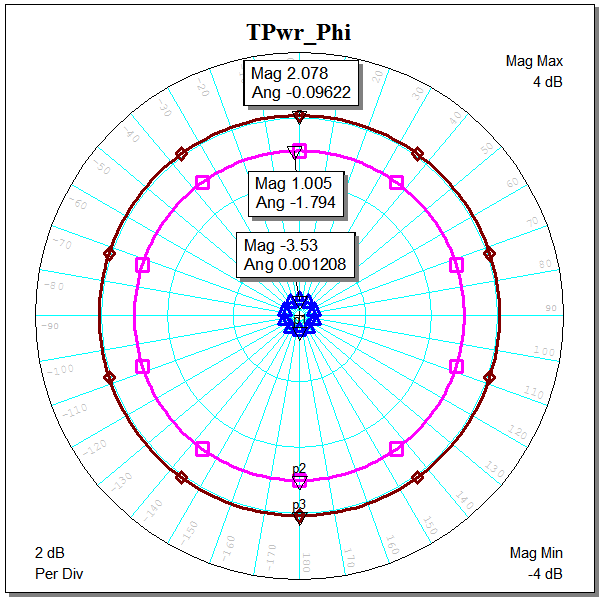
Fig.15 NAM in the azimuth plane
Which after all the above stated can be concluded? If initially, when designing a software package, the antenna and the influence of the board elements on it were thought out, then it would be possible to save time and money that was spent on a non-working sample.
I think the most interesting is to consider the situation described above with a specific example. So, we have a designed printed circuit board of a device that communicates over the radio channel in the frequency range 2.4 ... 2.48 GHz. This board is exactly the case when the antenna was placed on the residual principle, since The main task was to minimize the dimensions of the printed circuit board. After the manufacture of prototypes of PP and their installation, it turned out that the range of the radio channel is much less than the calculated one. At the same time, there were no problems with the circuit design of the created software. The method of elimination came to the conclusion that the antenna could be the culprit of the current situation.
Due to the small dimensions of the PP (15 mm by 20 mm), it was impossible to put a coaxial-microstrip junction (CMP) on it to connect the antenna directly to the measuring equipment. Therefore, it was decided to evaluate the characteristics of the antenna using special CAD systems. Fortunately, we have such an opportunity at the department. So, Figure 1 shows a 3D view of a printed circuit board with layers that affect the antenna characteristics of a printed emitter.
Fig. one
')
The number 1 denotes the area of inclusion of the device in the antenna.
And the following figures are the graphs of the characteristics of the antenna, calculated in the simulator. Let's look at a little more detailed graphics characteristics.
The VSWR schedule (Figure 2) allows to assess the degree of matching the antenna with the 50-ohm line (which, in fact, the signal is fed to the antenna). As can be seen from the graph, the minimum value of VSWR = 85 (and I would like the VSWR to be no more than 2).
Pic2
What does this mean? This suggests that 95% of all power supplied to the antenna is reflected back into the path. Thus, it is clear that the mismatched antenna radiates, at best, 5% of the input power, which leads to the fact that the range of the radio channel is significantly less than expected. Why it happens?
Figure 3 shows a graph of the complex impedances , from which it is clear that the antenna is inductance and its characteristic impedance is very far from 50 Ω.
Pic.3
And finally, the graphs of the radiation pattern (NF) in elevation (Figure 4) and azimuth (Figure 5) planes. Solely so that later it was possible to compare different versions of the implementation of the antenna.
Pic.4
Pic.5
Well, the most important question - what to do? In terms of austerity space on the PP options a bit. The option was recognized as a worker when the PCB increases by no more than 5 mm along the narrow side (i.e., new board dimensions of 20 mm by 20 mm). In this situation, it was decided to use the printed monopole, as the most compact. Figure 6 shows the modified topology with a new antenna.
Pic.6
Now everything looks a little better ...
This is how the VSWR looks like:
Fig.7
Here is the impedance diagram (the previous version is shown in blue, the new version is pink):
Fig.8
And NAM:
Fig.9 DN in elevation plane
Fig.10 DN in the azimuthal plane
As you can see, the new version is much better than the previous one. Along the edges of the working range, the maximum VSWR = 2.7: the power loss is about 20%. Of course, this option is a compromise between the dimensions of the printed circuit board and the antenna parameters, but it is 100% working.
In addition, the result can be even better if you do not bend the antenna, and straighten it and run along the edge of the board. For example, to do this (see Figure 11) and in this embodiment, the antenna can be placed along the body of the device.
Figure 11
At the same time, the obtained characteristics will be better than the previous version and much better than the original version (for the last version of the antenna, the graphics are brown).
Fig.12
From the graph in Figure 12 it can be seen that the last version of the antenna has the best VSWR = 1.25. Those. power loss is less than 1.5%.
Fig.13
Fig.14 Nam in elevation plane
Fig.15 NAM in the azimuth plane
Which after all the above stated can be concluded? If initially, when designing a software package, the antenna and the influence of the board elements on it were thought out, then it would be possible to save time and money that was spent on a non-working sample.
Source: https://habr.com/ru/post/235463/
All Articles