NAND Flash Analytics
Over the years, LSI experts have come to understand the importance of analytics interacting with NAND flash memory for optimizing performance and extending its life. In this regard, the company created a group that is studying the behavior of the NAND flash and describing the features of interaction with the LSI controllers. I bring to your attention an interview with an expert in this field, Bill Hunt, the chief engineer of the analytical department, which allows you to better understand what the group is doing.
Are all nand flash the same?
Of course not. NAND flash specifications, performance, and other characteristics vary not only from different manufacturers, they also differ between models of the same family. Often, even chips of the same model, produced at different times, especially at the very first stages and afterwards, differ. At times, manufacturers deliberately create different models of a single chip, addressed to different markets, for example, for corporations and custom solutions. Understanding the difference between NAND types is vital for building an effective solution.
')
How do NAND chips differ from different manufacturers?
There are two “levels” of difference between chip manufacturers: differences due to the difference in architecture, and differences between manufacturers using the same architecture. At manufacturers NAND with different design and production process the differences are cardinal. They consist of different pinouts, power requirements, block and page locations, addressing schemes, commands, recovery procedures for reading failures, and much more.
Some manufacturers use similar designs and manufacturing processes. But even in this case, their products may have significant operational differences. Each device can have unique properties depending on settings during production, commands, diagnostics. Even when using standard interfaces, such as ONFI and Toggle, there is no guarantee of the same operation. Each manufacturer has its own interpretation of these standards.
What are the differences between NAND chips of different generations?
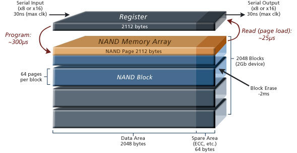
Reducing the geometry in the production of chips requires a new architecture. New architecture leads to changes in performance and specifications of the NAND device. The biggest changes are caused by an increase in the density of memory chips. For example, the size and location of blocks and pages must be changed to cope with the new architecture and increasing capacity. As memory cells become smaller and denser, error handling should also improve. Requirements for error correction codes (ECC) and backup sites are increasing. Also, NAND must adapt to the increasing rate at which bad blocks appear. The data transfer speed and performance of each new generation should also increase to meet user needs. This leads to changes in the timing specifications of the interface and the addition of new features. Overall, the performance of NAND deteriorates as the geometry is compacted, and it is critically important to understand these changes in order to develop more powerful and efficient ECC mechanisms.
What tests are performed in the LSI Flash Analytics Lab?

Flash Analytics Lab has two goals. First, we integrate NAND devices in SSDs with the LSI SandForce controller to make sure they work together. Second, we test NAND devices to see how flash memory works throughout its life cycle. We conduct testing in different operating modes. Understanding the behavior of NAND chips directly is critical to developing solutions with the reliability and performance demanded by the market.
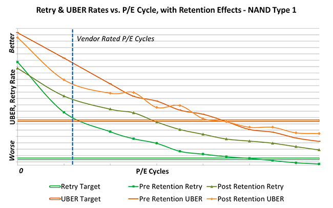
Are flash memory tests “outside” their passport life cycle?
Yes. NAND providers do not always share the results and methods of their endurance tests, so we have to collect this data ourselves. Usually, we perform write / erase cycles until the error level reaches a very large value, or a fatal failure occurs. We also measure other parameters, such as redundancy. Understanding the behavior of memory as it gets older is simply necessary in order to predict how devices will behave in real-world scenarios.
Source: https://habr.com/ru/post/234901/
All Articles