This is Science: News from graphene fields
The discovery of graphene and a description of its properties in 2004 brought the Nobel Prize to the creators of Game and Novoselov in 2010, but a decade after that very discovery, their followers intensively put into practice and offer various applications of such a unique material: from lubricant to vacuum transistors .
At the beginning of this year, the article “Graphene - life or death?” Was published, in which we understood the prospects and, in part, the consequences of the widespread introduction of graphene, as the basis of future microelectronics. Well, let's see what scientists today can offer us as part of the introduction of graphene to replace the already traditional materials.
Graphene at a glance
Graphene is a two-dimensional material consisting of sp 2 -hybridized carbon atoms, which has a number of interesting properties from the point of view of physics.
')
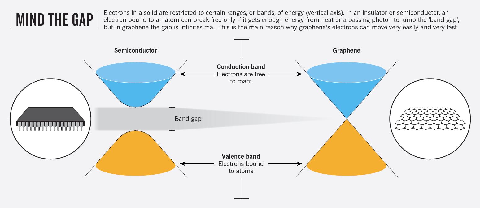
The most important and unique of them is electrical characteristics. On the one hand, graphene has a virtually zero forbidden band and very light electrons and holes, which makes it an ideal conductor capable of carrying signals faster than any other material on the planet. However, sp 2 hybridization of carbon atoms also allows its modification, for example, to obtain an insulator or a semiconductor. Plus, the transition between conducting and semiconducting states depends on the width of the graphene ribbon .
On the other hand, it is elastic, that is, bends, while demonstrating a unique and unattainable tensile strength - up to ~ 1000 GPa, which is almost 100 times higher than that of steel. A graphene rolled into a tube is a carbon nanotube, which can also be used in electronic devices; its diameter can vary from 1.5 nm to hundreds of nm.
And finally, it, graphene, is transparent, that is, just perfect as a substitute for expensive - mainly because of indium - ITO in modern displays and partly LEDs. However, two-dimensional systems themselves are not stable. Thus, the problem of creating a perfectly smooth graphene coating on any surface is a most difficult scientific and technical problem.
Perhaps, we will begin with the last property.
Graphene based LED or LED
Remarochka. If we consider the LED as such (in light bulbs, for example), then it does not potentially require an ITO substrate as an electrode, the thinnest metal contacts cope with this relatively well (I once wrote in a separate article about this). However, if you want to create a display on an array of LEDs, then in this case, replacing ITO is highly desirable and useful, including for improving display performance.
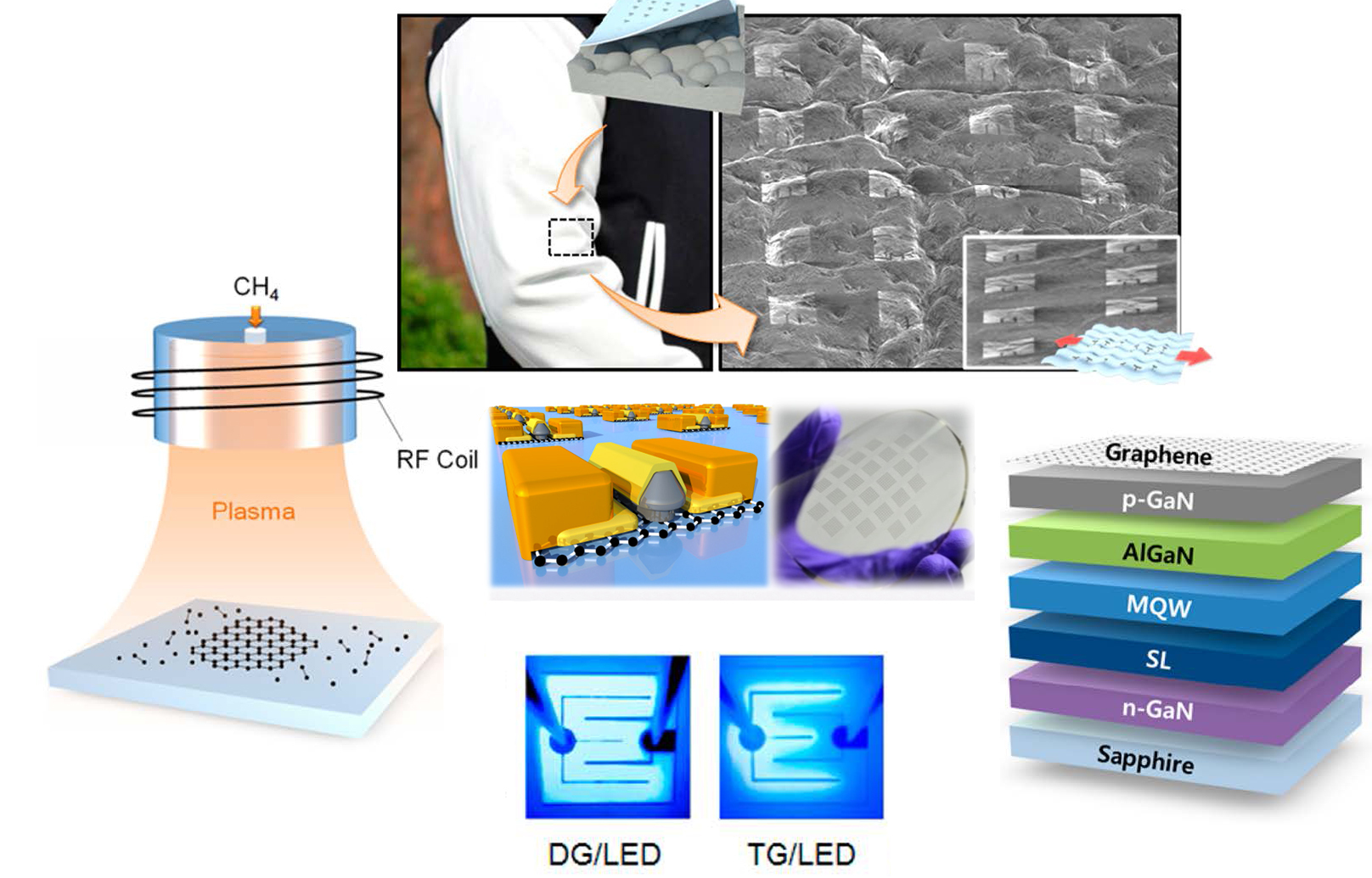
So, one of the industrial methods of coating graphene on various substrates is PECVD (or plasma-chemical deposition from the gas phase ). This technology is contained in the “injection” of a carrier gas of methane with its subsequent heating under the action of radio frequency radiation and the deposition of carbon on a cold substrate.
Here is a group of scientists from the Seoul National University and armed with this method of applying graphene coatings, suggesting a direct way to create bright blue diodes bypassing the stage of transferring graphene from the substrate to the substrate. In such LEDs, expensive ITO is replaced with a cheaper graphene substrate, and gallium nitride is used as the light-emitting layer, which is some industry standard.

From left to right: PECVD installation diagram; diode layout and main materials; current-voltage characteristic of the diode
Of course, by varying the duration of the PECVD process, it is possible to obtain a coating of graphene of different thickness and, accordingly, with different light transmission. However, the minimum number of layers, as shown in the figure below, allows you to get almost 100% transmission of light emitted by the LED, and, as a result, a greater external current output.
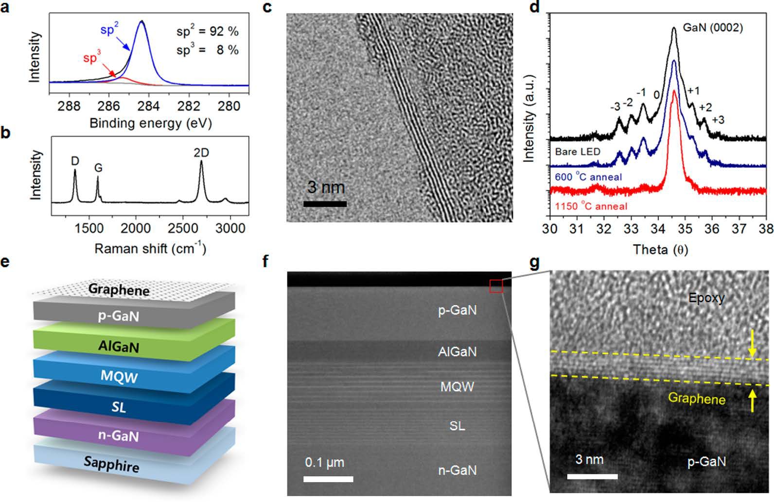
LED layered cake in the cut: from sapphire substrate to 5-6 graphene layers on the LED surface
The authors also tested for reproducibility and comparison with traditional technology of transferring graphene from one substrate, usually used for growth, to another, which will already stand in the final device:

ac) Test for reproducibility of results in one cycle. de) Comparison of graphene-based LEDs obtained by direct deposition (DG) and transfer, transfer of graphene from the substrate to the substrate (TG)
The results speak for themselves: with a relatively small variation in output power, the resulting LEDs confidently outperform the conventional, “standard” technology in maximum power at a given current (the comparison in Figure e).
The original article in ACSNano (DOI: 10.1021 / nn405477f)
Graphene RF-FET to communicate with wearable electronics
The main problem of truly wearable electronics, which is built into clothing and in no way attracts attention to itself - the combination of flexibility with certain characteristics. The teams of scientists of the following two articles devoted their work to finding a solution to this problem.
In the first of these, Taiwanese authors proposed an interesting way to create a field effect transistor on a flexible substrate, which could potentially become the basis for communication between individual elements of wearable electronics.
So, we need: graphene, transferred to a flexible PET substrate, a little aluminum to make a shutter and a drop of life-giving oxygen. Using lithography, we apply an aluminum gate on a strip of graphene, and then leave the device in a chamber with a couple of extra atmospheres of the purest O 2 . We don’t even have to do anything; chemistry and diffusion will do all the work for us, forming a barrier dielectric layer between aluminum and graphene. After that, it remains only to “dust”, that is, to apply the contacts themselves.
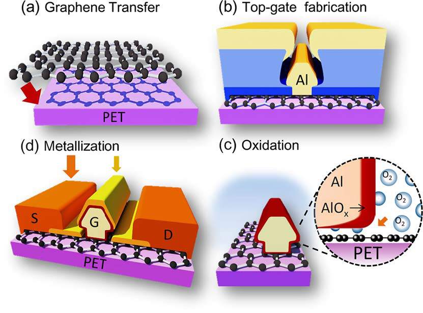
A rather simple and interesting scheme for the manufacture of a barrier dielectric layer in a graphene transistor.
And voila, the transistor assembly is ready. This is how it looks through the eye of an electron microscope:
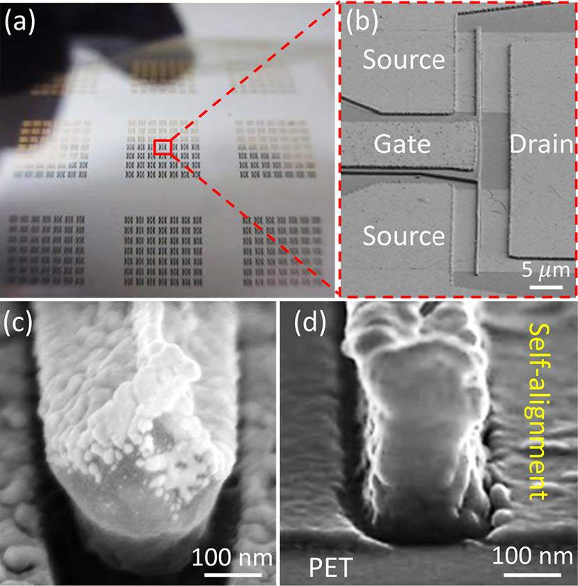
Optical photograph of a field-effect transistor (a) substrate and images of the transistors themselves, obtained using scanning electron microscopy
In order not to bore readers with rather boring technical details of testing this sample of a graphene-based field-effect transistor, let me immediately turn to potential development applications. The authors collected a frequency mixer based on the field-effect transistor and tested it, including during mechanical deformations.
More information about the principle of operation of the frequency mixer can be found here . For a brief explanation of the picture: LO is the known unmodulated frequency relative to which the conversion is performed, RF is the frequency that is converted / modulated, IF is used to send and receive low and high frequency signals.
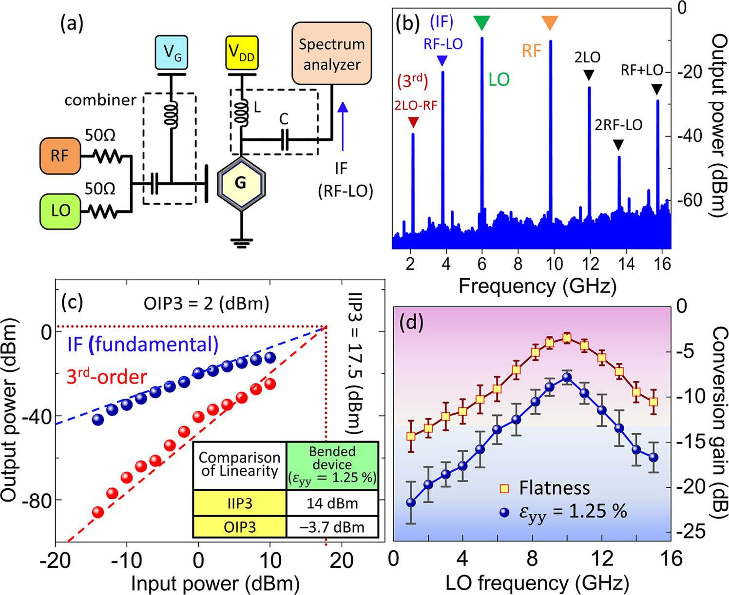
a) The electronic circuit of the mixer frequency based on a field-effect transistor. b) Radio frequency spectrum. cd) Radio Frequency Response
What does this give us? And it gives us a completely tiny transforming element of radio frequency technology, which can be used, for example, for NFC communication between, for example, individual devices inside smart clothes.
Original article in ACSNano (DOI: 10.1021 / nn5036087)
And as soon as we touched on the topic of wearable electronics, let's turn to the example of creating field-effect transistors on graphene-based fabrics.
Bend me completely grafen-style
Another group of South Korean scientists proposed a method for creating graphene ultra-thin transistors on an ultra-thin polymer substrate again, consisting of a special epoxy resin.
First, a thin polymer layer (SU-8) is applied on a conventional silicon substrate coated with a layer of silicon dioxide, on which transistors made of graphene are already “printed”, and then the SiO 2 layer is simply dissolved, thus separating the thinnest film from the substrate. In this case, the film can be transferred to virtually any surface, including tissue or skin. The total film thickness is less than 100 nm!
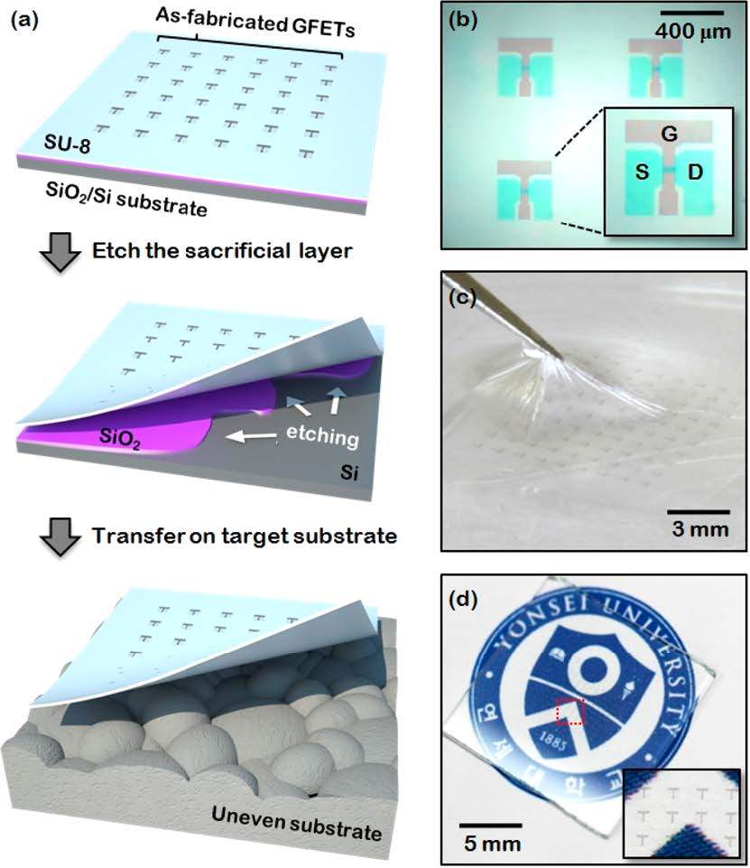
The process of creating a thin film with ultra-thin field-effect transistors
However, what problems await us with this transfer? That's right, this is not the surface uniformity: bends, cracks, creases - everything that can be present on the fabric surfaces. After all, changing the geometry of the transistor, we thereby change its transport properties, including charge mobility or distribution of the electric field at the gate, that is, it turns out that at the same nominal voltage the transistor in a bent state will suddenly begin to pass current, then, as in undeformed will lock it.
Fortunately, all these problems were avoided, and as a result it turned out that the position of the transistor (in a bend or on a flat surface of the fabric) does not significantly affect the electrical behavior of the transistor itself.

Testing transistors at different locations
As well as bends, stretching, folding the fabric in half:
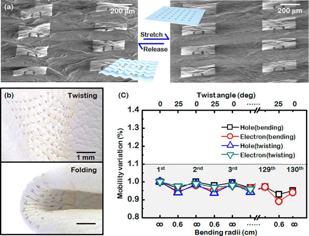
Testing transistors in bending, twisting, and stretching
And without thinking twice, the scientists decided using a developed technology to create a tactile sensor capable of recognizing a touch of 9 kPa, which is equivalent to a pressure of 0.1 atmosphere or 100 grams of force per cm 2 :
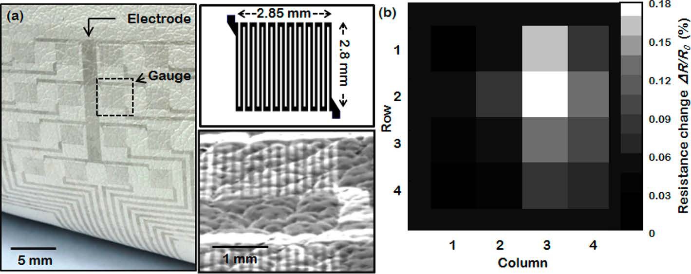
Tactile sensor capable of recognizing 0.1 kgf / cm 2
This technology can be used in smart clothes, as it does not require special equipment for applying (as they say, pasted and forgotten), including in the part of wearable and non-discomforting sensors of heartbeat, oxygen level and so on. But perhaps - what the
Original article in ACSNano (DOI: 10.1021 / nn503446f)
UPD: Thanks to koreec for providing a link to the Nobel laureate's article about graphene in Russian.
Full list of published articles This is Science on GeekTimes:
This is Science: Simple and Cheap Solar Energy
This is Science: Is graphene life or death?
This is Science: Blow and Get Electricity
This is Science: Silicon Electronics: Bend Me Completely!
This is Science: Resilient quantum dot display
This is Science: Putting triboelectricity at the service of humanity
This is Science: 3D optical printing moves to the micro level
This is Science: What's inside a neuromorph chip?
This is Science: News from graphene fields
This is Science: 3D lithography to masses
This is Science: The discharge of alkaline batteries or why the battery jumps
This is Science: microcannons and nano-core
This is Science: wearable electronics and triboelectricity. Part 1
This is Science: wearable electronics and triboelectricity. Part 2
Sometimes briefly, and sometimes not so much about the news of science and technology, you can read on my Telegram channel - welcome;)
Source: https://habr.com/ru/post/234401/
All Articles