A look at 10G Ethernet by an FPGA developer
Hello!
Many experts know that the top network equipment uses special chips to handle traffic. I take part in the development of such threshing machines and want to share my experience in creating such high-performance devices (with 10/40 / 100G Ethernet interfaces).
To create a new channel, networkers often take optics, a couple of SFP + modules, stick them into devices: the lights light up happily, packets start coming: the chip starts to transmit them to the recipients. But how does the chip get packets from the transmission medium? If interested, then welcome under cat.
Ethernet is a standard adopted by the IEEE association. 802.3 standards cover all possible Ethernet varieties (from 10M to 100G). Let's concentrate on the specific physical layer implementation: 10GBASE-R (“normal” 10G, no frills).
')

This figure shows the layers of the OSI model and how they are mapped to Ethernet sublayers.
Sub Levels:
PHY is divided into the following parts:
Terms:
For each type of physical layer, there can be its own implementation of individual PHY-sublevels: different coding is used, different transmission frequencies (wavelengths) are used, but a clear division into levels is everywhere traced. The presence of an environment-independent interface (XGMII) simplifies the development of chip application logic, since for any connection, the developer will get an XGMII somewhere. We’ll talk about what XGMII is about later.
The PMD sublayer is located closest to the environment: its tasks are solved by special modules that are well known to network specialists:
In this table, there is already a familiar abbreviation: XAUI. Let us leave the consideration of XENPAK / X2 in the middle of the article, and turn to the most popular modules: XFP and SFP +.
XFI and SFI actually represent the same interface: a differential pair, running at speeds from 9.95 to 11.10 gigabytes. The speed set is caused by the fact that several standards can use this interface: from 10GBASE-W WAN to 10GBASE-R over G.709. We are interested in 10GBASE-R LAN with a speed of 10.3125 gigabytes. One difpara is used for reception, the other for transmission.
The tasks of the PMA and PCS sublayers can be solved on a chip, where we will perform further processing of Ethernet packets (after we extract them from XGMII). Let me remind you that in the PMA sublayer it is necessary to select a clock frequency at the reception and deserialize the input signal. Such work can be performed by special hardware blocks that cannot be used for other tasks. These blocks are called transceivers. An entire article can go to their detailed description: who is interested, can see the block diagram of transceivers in Altera's FPGA.
After deserialization, the data falls into the PCS sublayer, where descrambling and decoding is performed (64b / 66b) and the data is sent as XGMII towards MAC. On the transfer, reverse actions are performed.
PCS can be implemented using special hardware blocks (Hard PCS) or with user-friendly logic (Soft PCS). Of course, this statement is valid only for FPGA: in ASICs, everything is done in hardware. FPGA manufacturers are laying PCS hardware blocks for standard protocols, saving the developer time and FPGA resources. The presence of such blocks is very appealing because many standard protocols work out of the box from experience, and for most of them the code is provided free by the FPGA manufacturer.

Transceivers in FPGA are expensive, an additional ten transceivers can significantly raise the price of a chip. There are cheaper chips with transceivers operating at lower speeds (they can serialize / deserialize data at lower frequencies). Another high-frequency interface, which is defined in section 4 of the 802.3 standard, is XAUI: 4 differential pairs with a transmission speed of 3.125 gigabytes (for one transmission line).
When using XAUI, the optional XGXS level arises, which allows you to separate the PHY and MAC from each other by distance. For example, perform in different chips.
The task of PMA and PCS in such a connection can be performed by special 10G transceivers (I assume that confusion may arise, because the “transceivers” exploded a bit earlier in FPGA, and now this term occurs. By the way, XFP / SFP + modules are also called transceivers .)
Examples of 10G transceivers:
This transceiver is a separate chip, placed between the XFP / SFP + module and “our” chip, which will process Ethernet packets. In fact, such a transceiver using PMA and PCS blocks converts XFI / SFI to XGMI, and then XGMII is converted to XAUI.
XAUI is fed to ASIC / FPGA, where transceivers are used, similar to those discussed earlier, but at a speed of 3.125G. The operation of the transceiver is different from the way it happens in 10G mode:
The XAUI PCS outputs the XGMII interface.
Some PHY transceivers can immediately issue an XGMII interface to the pins, and then the ASIC / FPGA transceivers should not be used:

This connection method has significant disadvantages:
As I promised, we got to these types of modules. It is easy to see that their connection is reduced to the second option, only without using an external transceiver chip. The module will take over the tasks of the PMD, PMA and PCS sublayers.
XGMII is defined in clause 46 of the 802.3 standard. This interface consists of independent transmit and receive. Each direction has a 32-bit data bus (RXD / TXD [31: 0]), four pilot signals (RXC / TXC [3: 0]) and a clock that carries the direction (RX_CLK / TX_CLK). The standard specifies that the data and pilot signals are analyzed on each edge of a clock (DDR). On the data bus goes the packet itself, the control signals determine the beginning help to “allocate” the beginning and end of the packet, as well as report on accidents.
The value of RX_CLK / TX_CLK is 156.25 MHz. The multiplication of 156.25 * 10 ^ 6 * 32 * 2 gives exactly 10 Gbit / s. Most often, clicks on both fronts of the clock drop from clicking, increasing the frequency or width of the data:
The lower the frequency, the easier it is to process this data and the more budget chips can be used. Only top-end (read, expensive) FPGAs can afford to work at frequencies of ~ 300 MHz.
In order to “pull out” of the XGMII packet, a special MAC core is used:
Of course, this kernel has a transmitting part, which the packet “converts” to the XGMII interface.
Most often, such a kernel is implemented using logic that is available for user tasks. However, there is a manufacturer of FPGA, which the MAC core implemented in hardware, saving resources for the user.
The MAC core, highlighting the packet from XGMII and placing the packet in the internal memory of the chip, "transfers" control of the packet to the applied logic of the chip: parsers, filters, switching systems, etc. For example, if the chip is on the network card and it will be decided that the packet must be sent to the host, it can be sent using PCIe to the RAM connected to the CPU.
With L1 to a greater extent we have to face circuit engineers, who build boards for devices. FPGA-programmers work with this only at the beginning of the rise of iron: when XGMII started working and all transceivers passed tests, we concentrate on how to handle the traffic. In one device made the connection in the first embodiment: SFI goes into the FPGA directly. In the other two on the second option (using a transceiver and XAUI). There is also a device that has a connection both directly to SFI and via XAUI, but without a transceiver (the FPGA is connected to another chip).
To use external transceivers (and indeed most specialized chips), you must sign the NDA. With this special problems often does not arise. Along with the NDA, various docks are issued, for example, chip registers settings. From the experience of working with transceivers from two different manufacturers, I note that when raising the iron in the first batch, some problems arise with the tuning of the transceiver, which are relatively quickly resolved: multifunction transceivers and sometimes to tune in the required mode of operation. Sometimes it happens that the documentation on the chips is very bad, and we have to go through different options, but the technical support does not respond or openly declares that it does not provide support for these chips.
One of the advantages of using a transceiver chip is that along with the documentation a set of firmware settings can be distributed, which must be loaded into the transceiver when installing a certain type of module. As far as I understand, these firmware produce a clever adjustment of equalizers, without which a certain type of modules will work with bit errors. One of these SFP + modules (with a limiting amplifier) was treated this way. If you connect without a transceiver, then such settings should be prepared by yourself for ASIC / FPGA, which can be a non-trivial task.
Having an interface that is independent of the transmission medium makes life a lot easier, because The code (application logic: parsers, generators, analyzers, filters, etc.) is very easy to port from old projects to new ones, because no matter what type of connection was used.
Connecting (and processing) 40G / 100G to ASIC / FPGA is similar to 10G, however, there are some nuances. If it is interesting, it will be possible to devote a separate article to this, however, it will not be big.
Take the usual UDP packet with the “Hello, habr!” Line and send it to the device to see how it will look on XGMII.

I have a disassembled device on the table, on which new features are most often tested: we use it for a good example. To do this, we will prepare a special firmware and connect a debugger to see the signals inside the chip. The 10G connection is made according to the second option: using an external transceiver, which sends XAUI data to the FPGA side. This two-channel transceiver: can work with two SFP +.

What does XGMII (and our package) look like inside the FPGA:
This device inside the FPGA uses a 72 bit XGMII bus operating on a positive edge of the frequency of 156.25 MHz.
Legend:
It can be seen that little is left to receive the Ethernet packet: find its beginning and end (by check characters) and cut out the excess: IDLE , PREAMBLE and TERM .
Thanks for your time and attention! If you have questions, ask without a doubt.
PS
I thank my colleagues in des333 and paulig for constructive criticism and advice.
Many experts know that the top network equipment uses special chips to handle traffic. I take part in the development of such threshing machines and want to share my experience in creating such high-performance devices (with 10/40 / 100G Ethernet interfaces).
To create a new channel, networkers often take optics, a couple of SFP + modules, stick them into devices: the lights light up happily, packets start coming: the chip starts to transmit them to the recipients. But how does the chip get packets from the transmission medium? If interested, then welcome under cat.
IEEE 802.3
Ethernet is a standard adopted by the IEEE association. 802.3 standards cover all possible Ethernet varieties (from 10M to 100G). Let's concentrate on the specific physical layer implementation: 10GBASE-R (“normal” 10G, no frills).
')
This figure shows the layers of the OSI model and how they are mapped to Ethernet sublayers.
Sub Levels:
- PHY is a physical sublayer.
- MAC is the medium access control sublayer.
PHY is divided into the following parts:
- PMD - Transmits and receives individual bits on a physical interface.
- PMA - provides serialization / deserialization of data, as well as the allocation of clocks from serial data (on reception)
- PCS - provides scrambling / descrambling, as well as encoding / decoding (64b / 66b) data blocks
- XGXS - XGMII Extender: Used when the PHY and MAC are at a distance from each other (optional).
- RECONCILIATION is a sublayer that translates XGMII into MAC signals.
Terms:
- Medium - transmission medium.
- MDI - interface dependent data transmission medium.
- XGMII - 10G interface, independent of the data transmission medium. The goal of XGMII is to provide a simple and low-cost connection between the PHY and the MAC.
- XAUI - 10G interface to connect to the transceiver.
For each type of physical layer, there can be its own implementation of individual PHY-sublevels: different coding is used, different transmission frequencies (wavelengths) are used, but a clear division into levels is everywhere traced. The presence of an environment-independent interface (XGMII) simplifies the development of chip application logic, since for any connection, the developer will get an XGMII somewhere. We’ll talk about what XGMII is about later.
PMD
The PMD sublayer is located closest to the environment: its tasks are solved by special modules that are well known to network specialists:
| Module type | Interface |
|---|---|
| XENPAK | XAUI |
| X2 | XAUI |
| XFP | Xfi |
| SFP + | SFI |
In this table, there is already a familiar abbreviation: XAUI. Let us leave the consideration of XENPAK / X2 in the middle of the article, and turn to the most popular modules: XFP and SFP +.
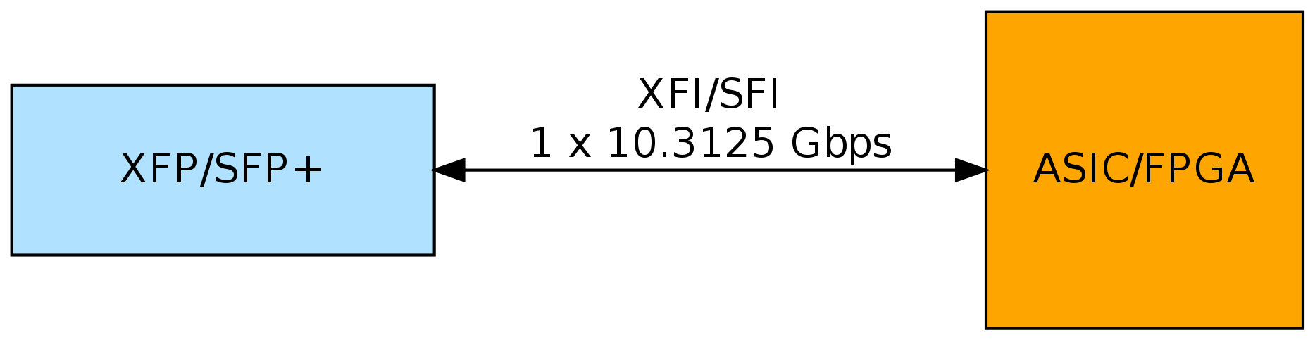
XFI / SFI
XFI and SFI actually represent the same interface: a differential pair, running at speeds from 9.95 to 11.10 gigabytes. The speed set is caused by the fact that several standards can use this interface: from 10GBASE-W WAN to 10GBASE-R over G.709. We are interested in 10GBASE-R LAN with a speed of 10.3125 gigabytes. One difpara is used for reception, the other for transmission.
XFI / SFI connects directly to ASIC / FPGA
The tasks of the PMA and PCS sublayers can be solved on a chip, where we will perform further processing of Ethernet packets (after we extract them from XGMII). Let me remind you that in the PMA sublayer it is necessary to select a clock frequency at the reception and deserialize the input signal. Such work can be performed by special hardware blocks that cannot be used for other tasks. These blocks are called transceivers. An entire article can go to their detailed description: who is interested, can see the block diagram of transceivers in Altera's FPGA.
After deserialization, the data falls into the PCS sublayer, where descrambling and decoding is performed (64b / 66b) and the data is sent as XGMII towards MAC. On the transfer, reverse actions are performed.
PCS can be implemented using special hardware blocks (Hard PCS) or with user-friendly logic (Soft PCS). Of course, this statement is valid only for FPGA: in ASICs, everything is done in hardware. FPGA manufacturers are laying PCS hardware blocks for standard protocols, saving the developer time and FPGA resources. The presence of such blocks is very appealing because many standard protocols work out of the box from experience, and for most of them the code is provided free by the FPGA manufacturer.
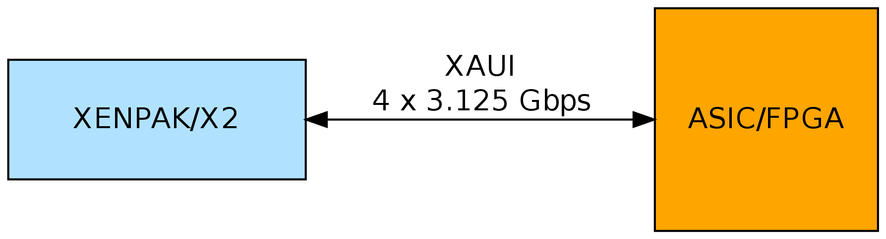
Connection via external transceiver chip
Transceivers in FPGA are expensive, an additional ten transceivers can significantly raise the price of a chip. There are cheaper chips with transceivers operating at lower speeds (they can serialize / deserialize data at lower frequencies). Another high-frequency interface, which is defined in section 4 of the 802.3 standard, is XAUI: 4 differential pairs with a transmission speed of 3.125 gigabytes (for one transmission line).
When using XAUI, the optional XGXS level arises, which allows you to separate the PHY and MAC from each other by distance. For example, perform in different chips.
The task of PMA and PCS in such a connection can be performed by special 10G transceivers (I assume that confusion may arise, because the “transceivers” exploded a bit earlier in FPGA, and now this term occurs. By the way, XFP / SFP + modules are also called transceivers .)
Examples of 10G transceivers:
- www.vitesse.com/products/productLine/10GE-PHYs
- www.marvell.com/transceivers/alaska-x-gbe
- www.broadcom.com/products/Physical-Layer/10-Gigabit-Ethernet-PHYs
This transceiver is a separate chip, placed between the XFP / SFP + module and “our” chip, which will process Ethernet packets. In fact, such a transceiver using PMA and PCS blocks converts XFI / SFI to XGMI, and then XGMII is converted to XAUI.
XAUI is fed to ASIC / FPGA, where transceivers are used, similar to those discussed earlier, but at a speed of 3.125G. The operation of the transceiver is different from the way it happens in 10G mode:
- Four transceivers are needed (four hardware blocks), because 4 differential pairs are used for this interface.
- XAUI PCS uses 8b / 10b encoding. The 10G PCS uses 64b / 66b.
The XAUI PCS outputs the XGMII interface.
Some PHY transceivers can immediately issue an XGMII interface to the pins, and then the ASIC / FPGA transceivers should not be used:
This connection method has significant disadvantages:
- High pin consumption: in the XGMII version, one chip uses at least 78 legs, versus 16 in the version with XAUI.
- Parallel interfaces may require alignment of the tracks on the board, which is sometimes nontrivial.
XENPAK / X2 connection
As I promised, we got to these types of modules. It is easy to see that their connection is reduced to the second option, only without using an external transceiver chip. The module will take over the tasks of the PMD, PMA and PCS sublayers.
XGMII
XGMII is defined in clause 46 of the 802.3 standard. This interface consists of independent transmit and receive. Each direction has a 32-bit data bus (RXD / TXD [31: 0]), four pilot signals (RXC / TXC [3: 0]) and a clock that carries the direction (RX_CLK / TX_CLK). The standard specifies that the data and pilot signals are analyzed on each edge of a clock (DDR). On the data bus goes the packet itself, the control signals determine the beginning help to “allocate” the beginning and end of the packet, as well as report on accidents.
The value of RX_CLK / TX_CLK is 156.25 MHz. The multiplication of 156.25 * 10 ^ 6 * 32 * 2 gives exactly 10 Gbit / s. Most often, clicks on both fronts of the clock drop from clicking, increasing the frequency or width of the data:
- Bus 36 bits (32 + 4) at a frequency of 312.5 MHz.
- Bus 72 bits (32 * 2 + 4 * 2) at a frequency of 156.25 MHz.
The lower the frequency, the easier it is to process this data and the more budget chips can be used. Only top-end (read, expensive) FPGAs can afford to work at frequencies of ~ 300 MHz.
In order to “pull out” of the XGMII packet, a special MAC core is used:
- Proprietary. After purchasing a license for such an IP core, you (most often) get the encrypted source code (without modification) and there is no particular restriction on the number of chips in which this core can be used. An example .
- With open source. Such kernels are very useful for beginners, since The code is open, and you can figure out how it works. License to use is determined separately. An example .
- Samopisnoe.
Of course, this kernel has a transmitting part, which the packet “converts” to the XGMII interface.
Most often, such a kernel is implemented using logic that is available for user tasks. However, there is a manufacturer of FPGA, which the MAC core implemented in hardware, saving resources for the user.
The MAC core, highlighting the packet from XGMII and placing the packet in the internal memory of the chip, "transfers" control of the packet to the applied logic of the chip: parsers, filters, switching systems, etc. For example, if the chip is on the network card and it will be decided that the packet must be sent to the host, it can be sent using PCIe to the RAM connected to the CPU.
Personal experience
With L1 to a greater extent we have to face circuit engineers, who build boards for devices. FPGA-programmers work with this only at the beginning of the rise of iron: when XGMII started working and all transceivers passed tests, we concentrate on how to handle the traffic. In one device made the connection in the first embodiment: SFI goes into the FPGA directly. In the other two on the second option (using a transceiver and XAUI). There is also a device that has a connection both directly to SFI and via XAUI, but without a transceiver (the FPGA is connected to another chip).
To use external transceivers (and indeed most specialized chips), you must sign the NDA. With this special problems often does not arise. Along with the NDA, various docks are issued, for example, chip registers settings. From the experience of working with transceivers from two different manufacturers, I note that when raising the iron in the first batch, some problems arise with the tuning of the transceiver, which are relatively quickly resolved: multifunction transceivers and sometimes to tune in the required mode of operation. Sometimes it happens that the documentation on the chips is very bad, and we have to go through different options, but the technical support does not respond or openly declares that it does not provide support for these chips.
One of the advantages of using a transceiver chip is that along with the documentation a set of firmware settings can be distributed, which must be loaded into the transceiver when installing a certain type of module. As far as I understand, these firmware produce a clever adjustment of equalizers, without which a certain type of modules will work with bit errors. One of these SFP + modules (with a limiting amplifier) was treated this way. If you connect without a transceiver, then such settings should be prepared by yourself for ASIC / FPGA, which can be a non-trivial task.
Having an interface that is independent of the transmission medium makes life a lot easier, because The code (application logic: parsers, generators, analyzers, filters, etc.) is very easy to port from old projects to new ones, because no matter what type of connection was used.
Connecting (and processing) 40G / 100G to ASIC / FPGA is similar to 10G, however, there are some nuances. If it is interesting, it will be possible to devote a separate article to this, however, it will not be big.
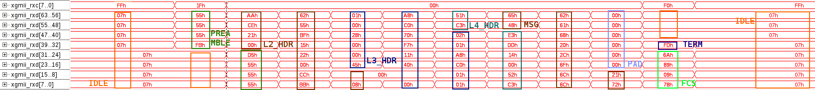
Hello, habr!
Take the usual UDP packet with the “Hello, habr!” Line and send it to the device to see how it will look on XGMII.
I have a disassembled device on the table, on which new features are most often tested: we use it for a good example. To do this, we will prepare a special firmware and connect a debugger to see the signals inside the chip. The 10G connection is made according to the second option: using an external transceiver, which sends XAUI data to the FPGA side. This two-channel transceiver: can work with two SFP +.
What does XGMII (and our package) look like inside the FPGA:
This device inside the FPGA uses a 72 bit XGMII bus operating on a positive edge of the frequency of 156.25 MHz.
Legend:
- xgmii_rxc - set of control signals.
- xgmii_rxd is a set of data signals (divided into bytes for convenience).
- IDLE - no packet transmission signals.
- PREAMBLE - preamble, marks the beginning of the packet transmission.
- L2_HDR - Level 2 Header: Ethernet.
- L3_HDR - Level 3 header: IP.
- L4_HDR - Level 4 header: UDP.
- MSG is our message (“Hello, habr!”).
- PAD - filling. Is present in the packet if the initial payload length was less than 60 bytes.
- FCS is the checksum of the packet. On it it is possible to determine whether the package was beaten during shipment or not.
- TERM - signal the end of the packet transmission.
It can be seen that little is left to receive the Ethernet packet: find its beginning and end (by check characters) and cut out the excess: IDLE , PREAMBLE and TERM .
Thanks for your time and attention! If you have questions, ask without a doubt.
PS
I thank my colleagues in des333 and paulig for constructive criticism and advice.
Source: https://habr.com/ru/post/234369/
All Articles