Repair Hard Disk Western Digital My Passport Essential SE 750 GB USB3.0
Good day to all.
Immediately I warn you, all actions described in the article are carried out at your own risk and peril, I, as the author of the article, are not responsible for the loss of information or damage to your device.
I somehow got an external USB 3.0 hard drive Western Digital My Passport 750 GB. I liked it because it has the ability to connect to a USB 3.0 port and its compact size. I used it a little over one year, and on one terrible day, it ceased to be detected by the system (both Windows and Linux). It happened because of the loss of voltage in the network. Then the voltage was applied, as a result of which, most likely, the hard disk failed. It was connected to an external USB hub, which is powered by an additional 5 V power supply. Not sure, of course, but in part, it must have been put out of order. But I don’t want to tell about this, but about how I was able to repair it.
This HDD has one board and all elements of a SATA controller and a SATA to USB 3.0 converter are built into it, which is why it turned out to be so compact. The fault was that this hard disk was defined in the system as a kind of device BAD PCB USB Device, and the system does not see the drive itself and any file system. Began to look in the Internet, what is the problem and how to solve it. As I found out from similar problems on the forums, the main problem in such hard drives (associated with the BAD PCB USB Device) is the failure of the converter (or you can call the controller) SATA to USB 3.0, and WD has external hard drives with such dimensions as above, but on other volumes. It turned out that WD, similar in construction, to WD, have different circuit design and configuration on the board. I didn’t find detailed instructions for reviving on my disk, so I had to perform repairs, as they say, in the image and likeness, relying on recommendations of other users of such disks or masters. Since the spindle in my disk, when connected to the USB socket through a cable, began to rotate, and the heads did not beat in convulsions, I concluded for myself that, most likely, there is still a sense of repair, and it is worth trying.
')
Judging by the forums, the malfunction was due to the failure of the SATA to USB 3.0 converter chip. The repair was that the hard disk has not completely lost its functions, which means that it can work if it is connected directly to the SATA interface or to the new SATA to USB 2.0 / 3.0 converter, as follows from these forum discussions:
Ixbt .
After reading the above forum and other sites proposed on it, I had hope, for which I am very grateful to the authors of articles and comments on the forums.
I will give a few pictures of printed circuit boards from hard drives for those links:
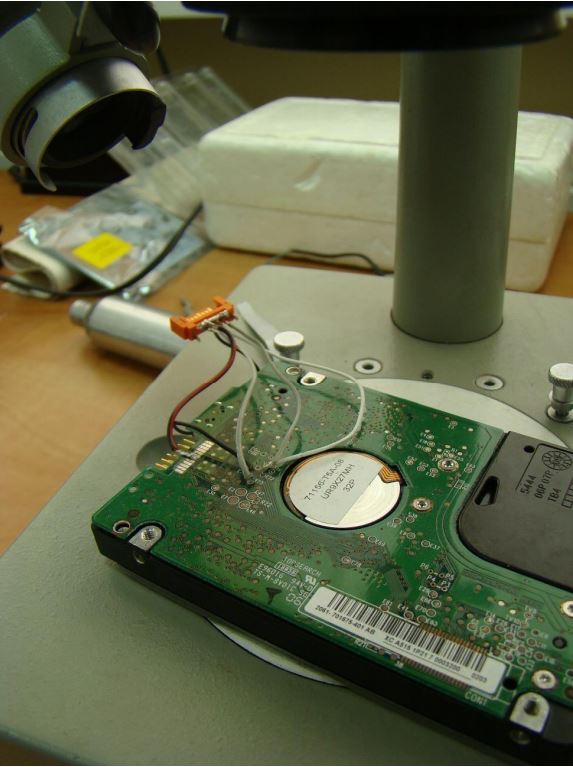
Fig. one

Fig. 2
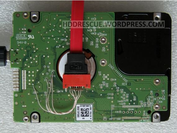
Fig. 3
The pictures show that the pads on the board are soldered to the conductors that lead to the SATA connector. It is not difficult to guess that the pads on the board are connected to the SATA interface circuits, namely, they are connected before the SATA to USB converter.
I unscrewed the motherboard from my HDD, and it turned out that the circuitry on this board was different from those in the above sites and in the above snapshots, but the principle became clear to me, and I saw the direction where to dig.
I immediately noticed the chips used on my motherboard and the main chips: the SATA controller and the SATA to USB converter differed from those shown in the links. Then, I also paid attention to the tracks (see position 1. in Figure 4 below), leading from the obvious SATA controller to the SATA to USB converter. Each of the tracks in its path passed through the contact pads with vias to the outer side of the board (pos 2, fig. 4). These tracks approached the capacitors C90, C91, C92, C93 (pos. 3, Fig. 4), and then the signal flowing through the tracks, passing through the capacitors, went to the SATA to USB converter chip, to which the connector is connected, to connect USB 3.0 power cord.
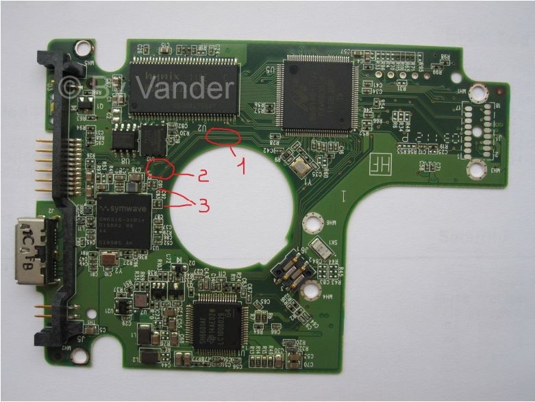
Fig. four
Now you need to make sure that these tracks are really SATA interface, and if so, find out what the polarity and purpose of these tracks are. For these purposes, I began to look for a description of the applied chips: 88i9146-TFJ2 (SATA controller), and SW6316-3VB14 (SATA to USB 3.0 converter). To my regret, I couldn’t find anything, for some reason these microcircuits are kept secret, or I wasn’t looking there, usually I use www.alldatasheet.com site to search for reference data on microchips (this is not for advertising purposes).
Then I began to look at the links that the search engine issued on request for the 88i9146-TFJ2 microchip, and found a photo of the board on this website: www.storagereview.com/western_digital_caviar_green_3tb_review_wd30ezrsdtl , on which this chip was applied, and on this board had this circuit, and this board had this board, and this board had this card, on which this chip was applied, on which this chip was applied, and on this board had this chip, and this board had this circuit board. SATA interface connections:
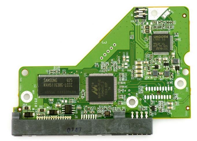
Fig. five
From this snapshot, I made sure that this chip is a SATA controller and that the tracks I immediately noticed on my motherboard are the SATA interface, as in Figure 5 you can see that the outputs of the IC 88i9146-TFJ2, which are connected to “Unusual” tracks on my motherboard lead to the SATA connector in fig. 5. Then, looking at the SATA connector base, I determined the polarity and purpose of the SATA interface tracks on my board, which means which pads of vias (Fig. 4, position 2) are responsible for which channel of the SATA interface (see Fig. 6 ).
Now there was a task to carefully solder the conductors to these tracks, which should be output to the SATA interface or a new SATA to USB converter. For myself, I bought a 2.5 AGE Star hard drive box with a built-in SATA to USB 3.0 converter. Since there was no direct SATA interface in my hard drive, but only a micro-B USB 3.0 connector, my hard drive could not fit into this box. In this regard, it was necessary to unsolder the USB 3.0 micro-B connector from the hard disk board, observing all precautions in terms of preventing mechanical loads on the board and thermal overheating. The USB connector in the hard disk board was soldered reliably, and in order not to overheat the board, I decided to file it, namely, cut it with a microdrill, in which a cutting disk (like the “Bulgarian”) inserted in dentistry was inserted on a special axis. "Grinder" on the side edges, I sawed the side racks of the connector, after which the connector became easier to unsolder "in parts." On the converter board of the new box, I also soldered the SATA + SATA power connector, which would also prevent my HDD from being packed into the box.

Fig. 6
Well, then it's small, you need to remove the SATA interface conductors from the HDD board, and solder the conductors with +5 V from the converter box of the new box.
For a start, I sealed off the capacitors (pos. 3, fig. 4), since they lead to a microcircuit that failed. I do not know the microcircuit nodes that have failed, and in order not to risk, the capacitors should have been removed, since Through them in the chip SW6316-3VB14, the useful signal of the SATA interface can be bridged, if the inputs of this chip are punched or somehow connected to the common wire.
The HDD board has very thin tracks and extremely small contact pads for vias, especially those holes that I needed for soldering (see Fig. 4, pos. 2). In my opinion, the diameter of these holes, taking into account the metallization, is about 0.3 mm, and the contact pad has a diameter, at best, 0.6 mm, which is very unreliable in terms of mechanical strength. Those. if I begin to solder the conductors to these tracks, then with one wrong move on forming the wire, I can easily disrupt this contact pad. I did the following:
1) neatly, in order not to touch the adjacent tracks, cleaned the contact pads of vias shown on fig. 2 from the solder mask (green coating) on both sides. 4 pos. 2 and fig. 6;
2) inserted thin copper clad wires, about 0.2 mm in diameter, into these holes;
3) soldered these wires from two sides, carefully so that the solder does not flow onto the adjacent tracks;
4) with a side cutter, biting off the excessively protruding ends of the wires.
Everything, now the mechanical strength of the contact pads is much more reliable, and the installation wire can now be soldered to these pads.
As an installation wire, I took the MGTF-0.07 wire, it is rather thin in diameter, has rather thin strands, which gives it flexibility, and most importantly has a heat-resistant fluoroplastic insulation, which is very important in order for the soldering not to melt and did not crawl bare the wire, because of which there may be a short circuit. I neatly cleaned and rounded the ends of the wires, and then soldered them to the contact pads so that there were no excess solder fluxes and that the solder drops had the lowest possible height above the board. This is done so that the drops do not rest on the body of the new box, which can break contact pads with wires or pierce the insulation of the box cover (if the cover is metal and insulated with a film, as in my case, a short circuit may occur). I also brought out the 5th wire GND for the interface (conditionally accepted by me the common wire for the SATA interface), and passed it along with 4 interface wires for the clamp from an insulated wire that I soldered to where the USB socket was previously 3.0 micro-B. The clamp can not be soldered, but it is recommended to make for more reliable fastening of the wires on the board so that they do not come off “with the roots”. It is also recommended that, at a distance of about 5 mm from the soldering points, glue the wires to the board with glue based on ethyl cyanoacrylate (the so-called Superglue), which securely and quickly fasten the wires to the board.
I connected the power wires to the hard drive board on the service connector, which is probably on it, which is made in the form of a double-row plug with 12 contacts (of the type PLD2-12-R). I determined the power contacts by a dial, first on the board I connected the multimeter probe to the common wire, and then I found a common wire on the pins of the connector. I also detected a +5 V power contact by dialing, but now I connected the probe on the board to the soldering point of the No. 1 USB 3.0 micro-B power connector, and found the power contact on the end connector with the second probe. I soldered the power wires directly to the connector pins and insulated with a PVC tube. All this can be seen in Figure 7.
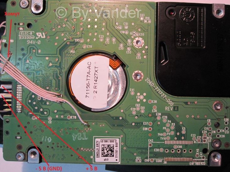
Fig. 7
After all the above operations, I finally soldered the wires to the SATA to USB 3.0 converter box of the new box, about which I’m not going to tell and describe here, because it may differ from one to another, depending on which box you purchase.
My hard drive was working, no information was lost from it, and all information is read without problems, i.e. no encryption "on the fly", as I read in different forums, the manufacturer did not provide for this model of the hard disk.
I hope that my article will be useful to someone.
Immediately I warn you, all actions described in the article are carried out at your own risk and peril, I, as the author of the article, are not responsible for the loss of information or damage to your device.
I somehow got an external USB 3.0 hard drive Western Digital My Passport 750 GB. I liked it because it has the ability to connect to a USB 3.0 port and its compact size. I used it a little over one year, and on one terrible day, it ceased to be detected by the system (both Windows and Linux). It happened because of the loss of voltage in the network. Then the voltage was applied, as a result of which, most likely, the hard disk failed. It was connected to an external USB hub, which is powered by an additional 5 V power supply. Not sure, of course, but in part, it must have been put out of order. But I don’t want to tell about this, but about how I was able to repair it.
This HDD has one board and all elements of a SATA controller and a SATA to USB 3.0 converter are built into it, which is why it turned out to be so compact. The fault was that this hard disk was defined in the system as a kind of device BAD PCB USB Device, and the system does not see the drive itself and any file system. Began to look in the Internet, what is the problem and how to solve it. As I found out from similar problems on the forums, the main problem in such hard drives (associated with the BAD PCB USB Device) is the failure of the converter (or you can call the controller) SATA to USB 3.0, and WD has external hard drives with such dimensions as above, but on other volumes. It turned out that WD, similar in construction, to WD, have different circuit design and configuration on the board. I didn’t find detailed instructions for reviving on my disk, so I had to perform repairs, as they say, in the image and likeness, relying on recommendations of other users of such disks or masters. Since the spindle in my disk, when connected to the USB socket through a cable, began to rotate, and the heads did not beat in convulsions, I concluded for myself that, most likely, there is still a sense of repair, and it is worth trying.
')
Judging by the forums, the malfunction was due to the failure of the SATA to USB 3.0 converter chip. The repair was that the hard disk has not completely lost its functions, which means that it can work if it is connected directly to the SATA interface or to the new SATA to USB 2.0 / 3.0 converter, as follows from these forum discussions:
Ixbt .
After reading the above forum and other sites proposed on it, I had hope, for which I am very grateful to the authors of articles and comments on the forums.
I will give a few pictures of printed circuit boards from hard drives for those links:
Fig. one
Fig. 2
Fig. 3
The pictures show that the pads on the board are soldered to the conductors that lead to the SATA connector. It is not difficult to guess that the pads on the board are connected to the SATA interface circuits, namely, they are connected before the SATA to USB converter.
I unscrewed the motherboard from my HDD, and it turned out that the circuitry on this board was different from those in the above sites and in the above snapshots, but the principle became clear to me, and I saw the direction where to dig.
I immediately noticed the chips used on my motherboard and the main chips: the SATA controller and the SATA to USB converter differed from those shown in the links. Then, I also paid attention to the tracks (see position 1. in Figure 4 below), leading from the obvious SATA controller to the SATA to USB converter. Each of the tracks in its path passed through the contact pads with vias to the outer side of the board (pos 2, fig. 4). These tracks approached the capacitors C90, C91, C92, C93 (pos. 3, Fig. 4), and then the signal flowing through the tracks, passing through the capacitors, went to the SATA to USB converter chip, to which the connector is connected, to connect USB 3.0 power cord.
Fig. four
Now you need to make sure that these tracks are really SATA interface, and if so, find out what the polarity and purpose of these tracks are. For these purposes, I began to look for a description of the applied chips: 88i9146-TFJ2 (SATA controller), and SW6316-3VB14 (SATA to USB 3.0 converter). To my regret, I couldn’t find anything, for some reason these microcircuits are kept secret, or I wasn’t looking there, usually I use www.alldatasheet.com site to search for reference data on microchips (this is not for advertising purposes).
Then I began to look at the links that the search engine issued on request for the 88i9146-TFJ2 microchip, and found a photo of the board on this website: www.storagereview.com/western_digital_caviar_green_3tb_review_wd30ezrsdtl , on which this chip was applied, and on this board had this circuit, and this board had this board, and this board had this card, on which this chip was applied, on which this chip was applied, and on this board had this chip, and this board had this circuit board. SATA interface connections:
Fig. five
From this snapshot, I made sure that this chip is a SATA controller and that the tracks I immediately noticed on my motherboard are the SATA interface, as in Figure 5 you can see that the outputs of the IC 88i9146-TFJ2, which are connected to “Unusual” tracks on my motherboard lead to the SATA connector in fig. 5. Then, looking at the SATA connector base, I determined the polarity and purpose of the SATA interface tracks on my board, which means which pads of vias (Fig. 4, position 2) are responsible for which channel of the SATA interface (see Fig. 6 ).
Now there was a task to carefully solder the conductors to these tracks, which should be output to the SATA interface or a new SATA to USB converter. For myself, I bought a 2.5 AGE Star hard drive box with a built-in SATA to USB 3.0 converter. Since there was no direct SATA interface in my hard drive, but only a micro-B USB 3.0 connector, my hard drive could not fit into this box. In this regard, it was necessary to unsolder the USB 3.0 micro-B connector from the hard disk board, observing all precautions in terms of preventing mechanical loads on the board and thermal overheating. The USB connector in the hard disk board was soldered reliably, and in order not to overheat the board, I decided to file it, namely, cut it with a microdrill, in which a cutting disk (like the “Bulgarian”) inserted in dentistry was inserted on a special axis. "Grinder" on the side edges, I sawed the side racks of the connector, after which the connector became easier to unsolder "in parts." On the converter board of the new box, I also soldered the SATA + SATA power connector, which would also prevent my HDD from being packed into the box.
Fig. 6
Well, then it's small, you need to remove the SATA interface conductors from the HDD board, and solder the conductors with +5 V from the converter box of the new box.
For a start, I sealed off the capacitors (pos. 3, fig. 4), since they lead to a microcircuit that failed. I do not know the microcircuit nodes that have failed, and in order not to risk, the capacitors should have been removed, since Through them in the chip SW6316-3VB14, the useful signal of the SATA interface can be bridged, if the inputs of this chip are punched or somehow connected to the common wire.
The HDD board has very thin tracks and extremely small contact pads for vias, especially those holes that I needed for soldering (see Fig. 4, pos. 2). In my opinion, the diameter of these holes, taking into account the metallization, is about 0.3 mm, and the contact pad has a diameter, at best, 0.6 mm, which is very unreliable in terms of mechanical strength. Those. if I begin to solder the conductors to these tracks, then with one wrong move on forming the wire, I can easily disrupt this contact pad. I did the following:
1) neatly, in order not to touch the adjacent tracks, cleaned the contact pads of vias shown on fig. 2 from the solder mask (green coating) on both sides. 4 pos. 2 and fig. 6;
2) inserted thin copper clad wires, about 0.2 mm in diameter, into these holes;
3) soldered these wires from two sides, carefully so that the solder does not flow onto the adjacent tracks;
4) with a side cutter, biting off the excessively protruding ends of the wires.
Everything, now the mechanical strength of the contact pads is much more reliable, and the installation wire can now be soldered to these pads.
As an installation wire, I took the MGTF-0.07 wire, it is rather thin in diameter, has rather thin strands, which gives it flexibility, and most importantly has a heat-resistant fluoroplastic insulation, which is very important in order for the soldering not to melt and did not crawl bare the wire, because of which there may be a short circuit. I neatly cleaned and rounded the ends of the wires, and then soldered them to the contact pads so that there were no excess solder fluxes and that the solder drops had the lowest possible height above the board. This is done so that the drops do not rest on the body of the new box, which can break contact pads with wires or pierce the insulation of the box cover (if the cover is metal and insulated with a film, as in my case, a short circuit may occur). I also brought out the 5th wire GND for the interface (conditionally accepted by me the common wire for the SATA interface), and passed it along with 4 interface wires for the clamp from an insulated wire that I soldered to where the USB socket was previously 3.0 micro-B. The clamp can not be soldered, but it is recommended to make for more reliable fastening of the wires on the board so that they do not come off “with the roots”. It is also recommended that, at a distance of about 5 mm from the soldering points, glue the wires to the board with glue based on ethyl cyanoacrylate (the so-called Superglue), which securely and quickly fasten the wires to the board.
I connected the power wires to the hard drive board on the service connector, which is probably on it, which is made in the form of a double-row plug with 12 contacts (of the type PLD2-12-R). I determined the power contacts by a dial, first on the board I connected the multimeter probe to the common wire, and then I found a common wire on the pins of the connector. I also detected a +5 V power contact by dialing, but now I connected the probe on the board to the soldering point of the No. 1 USB 3.0 micro-B power connector, and found the power contact on the end connector with the second probe. I soldered the power wires directly to the connector pins and insulated with a PVC tube. All this can be seen in Figure 7.
Fig. 7
After all the above operations, I finally soldered the wires to the SATA to USB 3.0 converter box of the new box, about which I’m not going to tell and describe here, because it may differ from one to another, depending on which box you purchase.
My hard drive was working, no information was lost from it, and all information is read without problems, i.e. no encryption "on the fly", as I read in different forums, the manufacturer did not provide for this model of the hard disk.
I hope that my article will be useful to someone.
Source: https://habr.com/ru/post/231459/
All Articles