Experience in the development and production of prototypes of BLE sockets
Hi, Habr!
I want to tell you how I developed and produced prototypes of sockets with the BLE interface. First of all, I would like to note that the device was chosen for the experiment - as a workshop on design and programming (to sharpen a pencil for working with 3D design of the case and printed circuit board, and to understand the functioning of the BLE stack from TI). An additional motivation was the presence of several successful projects on the kickstarter, developing such devices.
It was originally planned to create a device made in the form factor of a conventional socket adapter, that is, the most compact, and the device should be able to:
')
- manage the load (on and off - without dimming);
- read current consumption;
- turn on and off by timer / schedule;
- disconnect when communication is lost (when the user conditionally leaves the premises).
The circuitry of the device is rather trivial - a transformerless switching power supply, an integral current sensor, a bundle of antimistor + triac for switching the load and the brains of the SoC CC2541 device from Texas Instruments. At the time of choosing the element base, this was probably the most affordable chip with Bluetooth LE support, adequate debugging and development tools ( CC-debugger , sensortag , CC2541-DK-mini ) and a proven, though not the most convenient IAR compiler.
Altium designer summer 09 versions were used to design the circuitry and circuit board of the device, and later the project was moved to version 14. Despite the general acquaintance and a couple of implemented small projects, the lessons from Alexey Sabunin helped to move from P-cad to Altium. I strongly advise.
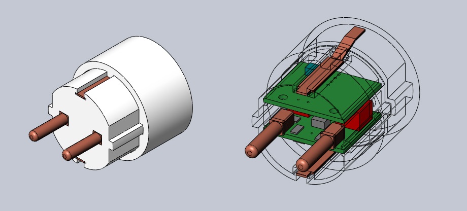
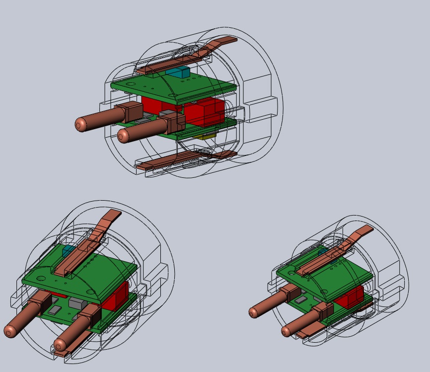
The dimensions of the device were determined based on the requirements of the form factor - hence the dimensions of the boards were determined and drawn (it immediately became clear that all components would not fit on one board - therefore it was decided to make two boards connected via pls-pbs connector. However, the question remains - whether all components fit on the boards, how to assemble them, so that the components from the neighboring boards do not touch each other, so that the power elements also do not touch the components and that all the stuffing fits into the size of the device? SolidWorks came to the rescue my opinion, the most adequate means of 3D design.
Fortunately, there is the mutual compatibility of AD with 3D design tools using .step files. It is noteworthy that only SolidWorks in the sp3 version of 2014 could adequately display the colors of the parts assigned in Altium Designer. What is the problem for me is still covered in darkness. So, after drawing in 3D parts of the case and several iterations of changing the layout of the boards, the assembly of the device began to look something like this:
Now it remains only to produce a device.
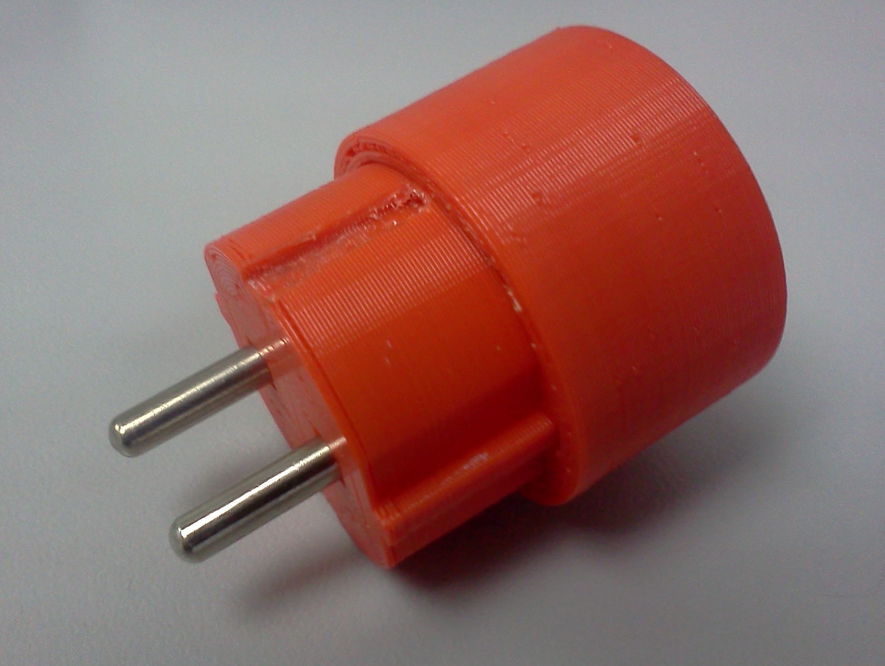
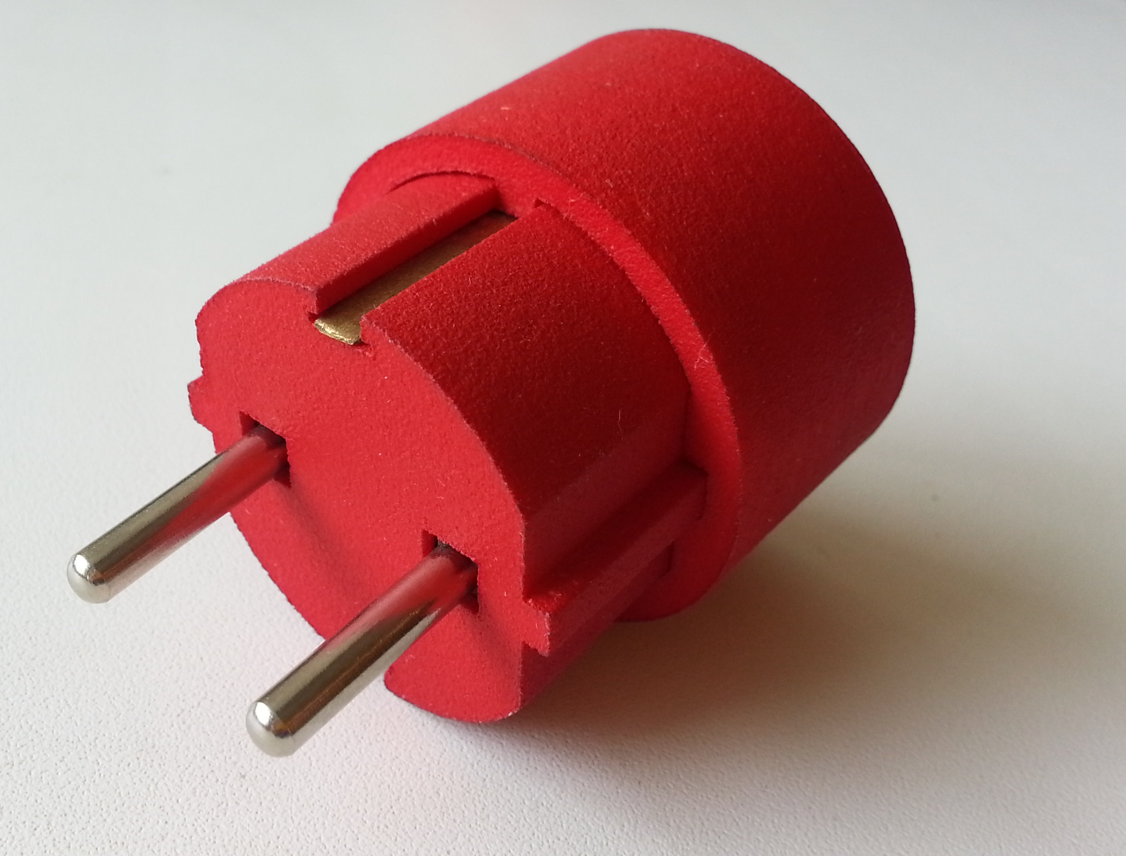
Traditionally I order exemplary quantities of printed circuit boards in Rezonite . Not that it is very cheap, but always qualitatively and on time, and industrial batches are produced quite at the market price. I also traditionally buy electronic components in two places - Kompele , where there is almost everything, and local Promelectronics , where you can almost always buy something that is not in Kompele. Separate attention deserves the first experience of 3D printing of body parts. Printing was made familiar to FDM technology. The result was a surprisingly positive red rosette:
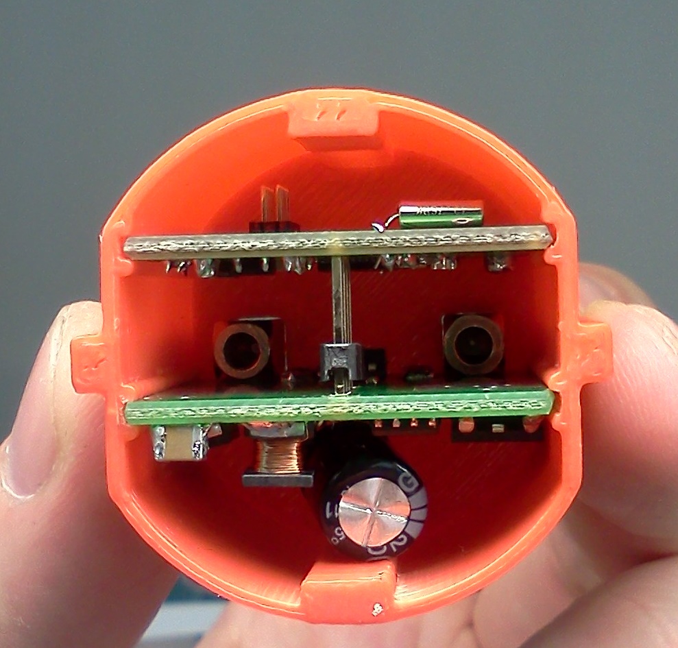
After soldering and assembly of parts:
While waiting for the boards and electronic components, work began on the BLE profile for the device. As it turned out, the TI stack for BLE looks much worse than the outside - the implementation of its own applications is not difficult, despite the relatively large amount of code for the 8051 platform.
The result was quite a workable device - it really performs all the declared functions, while being placed in the stated envelope. However, a few problems and questions left the prototype:
- how to fasten the case parts to each other? Should there be a collapsible connection?
- how to make grounding?
- How to improve the quality of the signal from the current sensor? Is this power noise or is the current sensor inaccurate?
I and my friends liked the product so much that it was decided to make a commercially packaged product. This involved resolving issues:
- writing software for smartphones;
- housing for mass production (for the manufacture of the mold);
- increase the maximum switching power (up to 2.5 kW versus 1.2 kW).
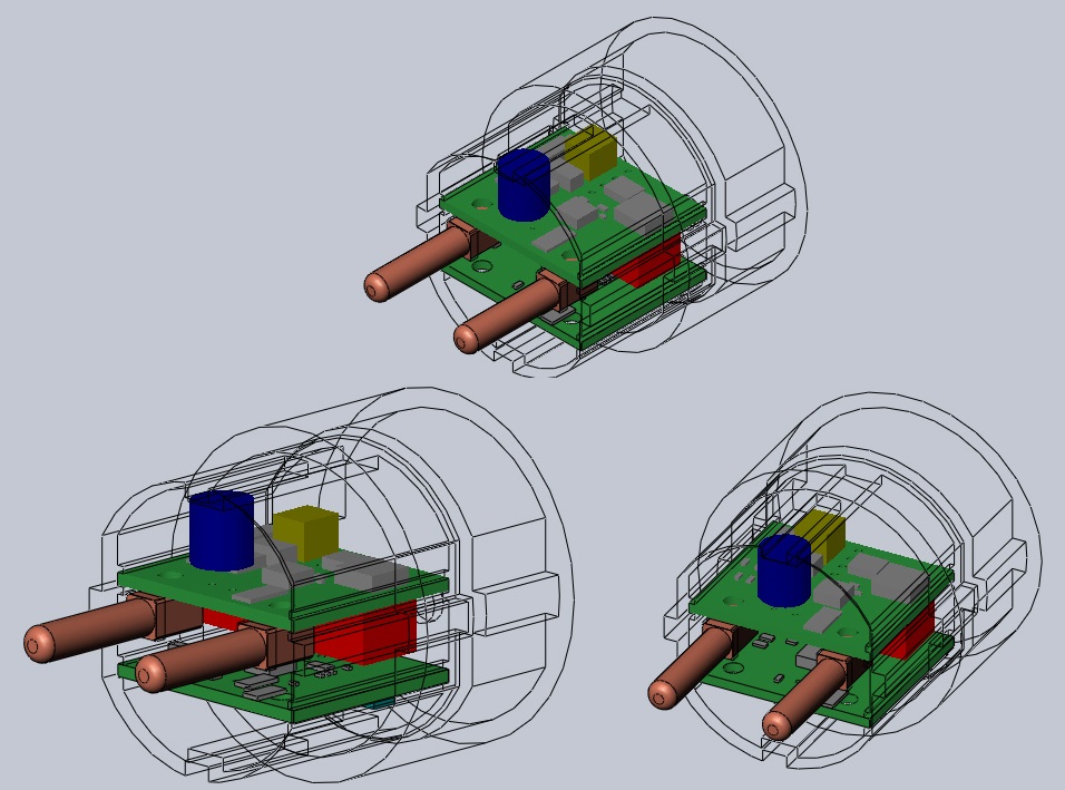
And the first thing with which it was necessary to decide - whether to make the case collapsible. By the will of fate, I do not trust the "latches" and similar compounds, so the option remained essentially the same - screw connection. But unfortunately, there was no option how to organize such a connection. Several types of screw rivets were tried, but none of them showed reliable fixation in thin plastic. In the absence of other options, it was decided to make the new building non-separable - with adhesive bonding. In addition, several structural elements were added for installing and fixing the ground. As a result, the assembly began to look something like this:
The power path was also redesigned for a maximum load of up to 3 kW (in fact, the triac in D2PAK changed the triac in DPAK), which resulted in several more PCB layout operations. Since printed using the FDM method could not boast of either dimensional accuracy or surface quality, it was decided to print cases using the SLS technology. The order was placed in the service i.materialise.com (more budget compared to domestic counterparts). However ... UPS Free Shipping had a black side - the order was in the UPS warehouse in Moscow 26! days than violated all my plans. The new circuitry also failed: an elementary error (confused contacts of a triac) cost me a lot of nerves and spoiled the entire internal aesthetics of the prototypes. In general, the new devices look like this:


Now I am busy reworking the board and searching for like-minded people in order to bring the product to the market. First of all, applications for mobile platforms are needed. Join now!
I want to tell you how I developed and produced prototypes of sockets with the BLE interface. First of all, I would like to note that the device was chosen for the experiment - as a workshop on design and programming (to sharpen a pencil for working with 3D design of the case and printed circuit board, and to understand the functioning of the BLE stack from TI). An additional motivation was the presence of several successful projects on the kickstarter, developing such devices.
1. Functional device
It was originally planned to create a device made in the form factor of a conventional socket adapter, that is, the most compact, and the device should be able to:
')
- manage the load (on and off - without dimming);
- read current consumption;
- turn on and off by timer / schedule;
- disconnect when communication is lost (when the user conditionally leaves the premises).
2. Circuit design and PCB
The circuitry of the device is rather trivial - a transformerless switching power supply, an integral current sensor, a bundle of antimistor + triac for switching the load and the brains of the SoC CC2541 device from Texas Instruments. At the time of choosing the element base, this was probably the most affordable chip with Bluetooth LE support, adequate debugging and development tools ( CC-debugger , sensortag , CC2541-DK-mini ) and a proven, though not the most convenient IAR compiler.
Altium designer summer 09 versions were used to design the circuitry and circuit board of the device, and later the project was moved to version 14. Despite the general acquaintance and a couple of implemented small projects, the lessons from Alexey Sabunin helped to move from P-cad to Altium. I strongly advise.
The dimensions of the device were determined based on the requirements of the form factor - hence the dimensions of the boards were determined and drawn (it immediately became clear that all components would not fit on one board - therefore it was decided to make two boards connected via pls-pbs connector. However, the question remains - whether all components fit on the boards, how to assemble them, so that the components from the neighboring boards do not touch each other, so that the power elements also do not touch the components and that all the stuffing fits into the size of the device? SolidWorks came to the rescue my opinion, the most adequate means of 3D design.
3. 3D design and assembly of the device
Fortunately, there is the mutual compatibility of AD with 3D design tools using .step files. It is noteworthy that only SolidWorks in the sp3 version of 2014 could adequately display the colors of the parts assigned in Altium Designer. What is the problem for me is still covered in darkness. So, after drawing in 3D parts of the case and several iterations of changing the layout of the boards, the assembly of the device began to look something like this:
Now it remains only to produce a device.
4. The first prototype
Traditionally I order exemplary quantities of printed circuit boards in Rezonite . Not that it is very cheap, but always qualitatively and on time, and industrial batches are produced quite at the market price. I also traditionally buy electronic components in two places - Kompele , where there is almost everything, and local Promelectronics , where you can almost always buy something that is not in Kompele. Separate attention deserves the first experience of 3D printing of body parts. Printing was made familiar to FDM technology. The result was a surprisingly positive red rosette:
After soldering and assembly of parts:
While waiting for the boards and electronic components, work began on the BLE profile for the device. As it turned out, the TI stack for BLE looks much worse than the outside - the implementation of its own applications is not difficult, despite the relatively large amount of code for the 8051 platform.
The result was quite a workable device - it really performs all the declared functions, while being placed in the stated envelope. However, a few problems and questions left the prototype:
- how to fasten the case parts to each other? Should there be a collapsible connection?
- how to make grounding?
- How to improve the quality of the signal from the current sensor? Is this power noise or is the current sensor inaccurate?
I and my friends liked the product so much that it was decided to make a commercially packaged product. This involved resolving issues:
- writing software for smartphones;
- housing for mass production (for the manufacture of the mold);
- increase the maximum switching power (up to 2.5 kW versus 1.2 kW).
5. Second iteration of prototyping
And the first thing with which it was necessary to decide - whether to make the case collapsible. By the will of fate, I do not trust the "latches" and similar compounds, so the option remained essentially the same - screw connection. But unfortunately, there was no option how to organize such a connection. Several types of screw rivets were tried, but none of them showed reliable fixation in thin plastic. In the absence of other options, it was decided to make the new building non-separable - with adhesive bonding. In addition, several structural elements were added for installing and fixing the ground. As a result, the assembly began to look something like this:
The power path was also redesigned for a maximum load of up to 3 kW (in fact, the triac in D2PAK changed the triac in DPAK), which resulted in several more PCB layout operations. Since printed using the FDM method could not boast of either dimensional accuracy or surface quality, it was decided to print cases using the SLS technology. The order was placed in the service i.materialise.com (more budget compared to domestic counterparts). However ... UPS Free Shipping had a black side - the order was in the UPS warehouse in Moscow 26! days than violated all my plans. The new circuitry also failed: an elementary error (confused contacts of a triac) cost me a lot of nerves and spoiled the entire internal aesthetics of the prototypes. In general, the new devices look like this:
Now I am busy reworking the board and searching for like-minded people in order to bring the product to the market. First of all, applications for mobile platforms are needed. Join now!
Source: https://habr.com/ru/post/231289/
All Articles