How to calculate 2 + 2 using electromagnetic relays
Last time I briefly described how the first module of my (future) computer was created on electromagnetic relays - an arithmetic logic unit. Now I want to talk a little about the principles of operation of this ALU, or rather, how the execution of logical and arithmetic operations is arranged.

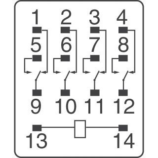
Electromagnetic relays consist of a winding, an anchor and switches. When a current in the winding occurs, it attracts an anchor to itself, and the switch transfers switches from one state to another. The picture above shows how the relays used in the ALU look, and the picture below shows the purpose of their contacts.
')
These relays have 4 switches each. When the current in the winding does not flow, the switches interconnect the contacts 1-9, 2-10, 3-11 and 4-12. If we apply voltage to the winding (in my case it is 24V), then the position of the switches will change to 5-9, 6-10, 7-11, 8-12.
In order to draw the diagrams of computer components, I used the same relay notation as in the HPRC documentation:
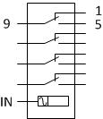
Here, only one of the conductors connected to the coil is drawn, because the second is always grounded, and therefore there is no sense in labeling it on the circuit. Since I used the relay with the LED on indicators, it clearly determined which coil contact is used as “+” and which one as “-”.
In semiconductor logic circuits, a low voltage level means a logical “0”, and a high voltage means a logical “1”. For example, in CMOS circuits, a given input is connected to the “ground” if it is necessary to supply a logical “0” to it.
In circuits on electromagnetic relays, everything is somewhat simpler. If we take the “1” voltage level, including the relay, then “0” can take any voltage, at which the relay is turned off, or no connection at all. In the second case, the relay will also turn off, as planned. Thus, the supply voltage (in my case, this is 24 V) is taken as “1”, and the absence of connection to the supply circuit is taken as “0”. This method allows you to easily manage signals by connecting / disconnecting to the power supply conductors.
Another difference between electromagnetic relays and semiconductor logic is the load capacity of the outputs. It is limited only by the capacity of the power supply, i.e. An unlimited (within reasonable limits, of course) number of inputs can be connected to any relay output, which simplifies the design of the device.
The principles on which I built the ALU, for the most part, were borrowed from the HPRC detailed description . And this computer, in turn, is partially based on the ideas of Konrad Zuse of the 1941 model. In particular, from there and originates.
The adder used in my ALU was coined by Konrad Zuse for his Z3 car, built in military Germany. Such an adder consists of 8 series-connected 1-bit adders. At the input of each of them are two bits of operands, as well as bits of the carry and inverted carry. At the output, each 1-bit adder gives the result of the calculation, that is, the sum of the input bits, taking into account the carry. In addition, the transfer and the inverted transfer are applied to the next adder.
In order for this circuit to be able to complete the calculations, it is necessary that the time elapses for switching 8 series-connected relays. The full adder circuit is shown in the picture:
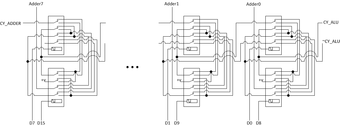
This is what happens to the circuit, if the admittance of the adder is 2 and 2 (red are the conductors to which the supply voltage is applied). Two relays corresponding to the first bits of the operands switched, and the rest remained in the initial state:

I also completely copied the logic module from HPRC. Bitwise logical operations are performed in parallel for all 8 bits of the result immediately. Since all bits are independent, the circuit runs faster than the adder (although it is almost impossible to notice). The logic module performs NOT, AND, OR, and EXCLUSIVE OR operations (they are also NOT, AND, OR, and XOR).
Logical does NOT work like this: the input of the logic element is connected to the relay coil; a power supply is connected to one of the inputs; the output of the element is a normally closed contact for this input. Thus, when “1” is applied to the input, the relay switches and the power supply is disconnected from the output contact:

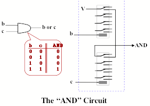
Logical AND is implemented using a serial connection of two normally open contacts, each of which is controlled by one of the input element:
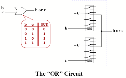
The method used to represent logical values using electrical signals allows the OR operation to be performed using “mounting OR” simply by connecting the corresponding wires:
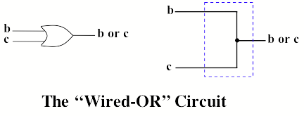
But this scheme has one drawback - the value of one of the input signals may affect the other (and each of these wires can be connected somewhere else). For example, in the figure below, b = 1 will result in “1” not only at both outputs, but also at inputs c and d, even if c and d themselves are equal to “0”.
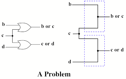
The problem is solved by duplicating signals with normally open relay contacts, to the coils of which these signals are connected:
The complete logic module diagram looks like this:

In addition to the listed logical operations, this circuit also generates input signals for the shear modulus. This is necessary for the same reason that in most cases it is impossible to use a simple “mounting OR” - the work of the shear module may affect its input signals.
I did not have anyone to copy the subtractor module (since HPRC simply does not know how to subtract), so I took truth tables for single-bit adders and subtractors, compared them, and redid the adder circuit into a subtractor circuit. It turned out very similar to the adder design:

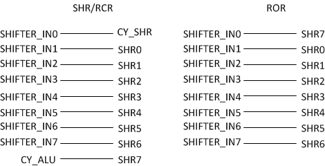
The module performing the shifts is unique in that it consists only of wires. I only needed right shift operations (left shift is easily done using the addition operation): right shift with and without translation, and also rotation to the right. Thus, to perform these operations, it is enough to connect the input signals from the data bus to the output of the internal bus of the ALU in the desired order:
In conclusion, I will give a picture that shows what the result of calculating all operations is for operands 3 and 2 (the selected values can be seen from the toggle switches in the lower left corner, as well as from the indicators of the relay in each of the modules). This is possible, since the operation of the modules does not depend on which operation is selected (it only depends on which of the results is clicked).

Here are described all the blocks that perform logical and arithmetic operations in the ALU, which will be included in the computer for electromagnetic relays .
I started this work with ALU, because it includes a lot of things that will be used in other modules: elementary logic operations, adder (PC increment operation will be performed by a special increment block), as well as bus commutation blocks and registers.
In the next article I plan to describe the logical structure of the ALU, as well as address the planned architecture and command system of the computer as a whole.
How does the electromagnetic relay
Electromagnetic relays consist of a winding, an anchor and switches. When a current in the winding occurs, it attracts an anchor to itself, and the switch transfers switches from one state to another. The picture above shows how the relays used in the ALU look, and the picture below shows the purpose of their contacts.
')
These relays have 4 switches each. When the current in the winding does not flow, the switches interconnect the contacts 1-9, 2-10, 3-11 and 4-12. If we apply voltage to the winding (in my case it is 24V), then the position of the switches will change to 5-9, 6-10, 7-11, 8-12.
In order to draw the diagrams of computer components, I used the same relay notation as in the HPRC documentation:
Here, only one of the conductors connected to the coil is drawn, because the second is always grounded, and therefore there is no sense in labeling it on the circuit. Since I used the relay with the LED on indicators, it clearly determined which coil contact is used as “+” and which one as “-”.
Binary logic in circuits on electromagnetic relays
In semiconductor logic circuits, a low voltage level means a logical “0”, and a high voltage means a logical “1”. For example, in CMOS circuits, a given input is connected to the “ground” if it is necessary to supply a logical “0” to it.
In circuits on electromagnetic relays, everything is somewhat simpler. If we take the “1” voltage level, including the relay, then “0” can take any voltage, at which the relay is turned off, or no connection at all. In the second case, the relay will also turn off, as planned. Thus, the supply voltage (in my case, this is 24 V) is taken as “1”, and the absence of connection to the supply circuit is taken as “0”. This method allows you to easily manage signals by connecting / disconnecting to the power supply conductors.
Another difference between electromagnetic relays and semiconductor logic is the load capacity of the outputs. It is limited only by the capacity of the power supply, i.e. An unlimited (within reasonable limits, of course) number of inputs can be connected to any relay output, which simplifies the design of the device.
Computational Blocks ALU
The principles on which I built the ALU, for the most part, were borrowed from the HPRC detailed description . And this computer, in turn, is partially based on the ideas of Konrad Zuse of the 1941 model. In particular, from there and originates.
Adder
The adder used in my ALU was coined by Konrad Zuse for his Z3 car, built in military Germany. Such an adder consists of 8 series-connected 1-bit adders. At the input of each of them are two bits of operands, as well as bits of the carry and inverted carry. At the output, each 1-bit adder gives the result of the calculation, that is, the sum of the input bits, taking into account the carry. In addition, the transfer and the inverted transfer are applied to the next adder.
In order for this circuit to be able to complete the calculations, it is necessary that the time elapses for switching 8 series-connected relays. The full adder circuit is shown in the picture:
This is what happens to the circuit, if the admittance of the adder is 2 and 2 (red are the conductors to which the supply voltage is applied). Two relays corresponding to the first bits of the operands switched, and the rest remained in the initial state:
Logic module
I also completely copied the logic module from HPRC. Bitwise logical operations are performed in parallel for all 8 bits of the result immediately. Since all bits are independent, the circuit runs faster than the adder (although it is almost impossible to notice). The logic module performs NOT, AND, OR, and EXCLUSIVE OR operations (they are also NOT, AND, OR, and XOR).
Logical does NOT work like this: the input of the logic element is connected to the relay coil; a power supply is connected to one of the inputs; the output of the element is a normally closed contact for this input. Thus, when “1” is applied to the input, the relay switches and the power supply is disconnected from the output contact:
Logical AND is implemented using a serial connection of two normally open contacts, each of which is controlled by one of the input element:
The method used to represent logical values using electrical signals allows the OR operation to be performed using “mounting OR” simply by connecting the corresponding wires:
But this scheme has one drawback - the value of one of the input signals may affect the other (and each of these wires can be connected somewhere else). For example, in the figure below, b = 1 will result in “1” not only at both outputs, but also at inputs c and d, even if c and d themselves are equal to “0”.
The problem is solved by duplicating signals with normally open relay contacts, to the coils of which these signals are connected:
The complete logic module diagram looks like this:
In addition to the listed logical operations, this circuit also generates input signals for the shear modulus. This is necessary for the same reason that in most cases it is impossible to use a simple “mounting OR” - the work of the shear module may affect its input signals.
Subtractor
I did not have anyone to copy the subtractor module (since HPRC simply does not know how to subtract), so I took truth tables for single-bit adders and subtractors, compared them, and redid the adder circuit into a subtractor circuit. It turned out very similar to the adder design:
Shear modulus
The module performing the shifts is unique in that it consists only of wires. I only needed right shift operations (left shift is easily done using the addition operation): right shift with and without translation, and also rotation to the right. Thus, to perform these operations, it is enough to connect the input signals from the data bus to the output of the internal bus of the ALU in the desired order:
In conclusion, I will give a picture that shows what the result of calculating all operations is for operands 3 and 2 (the selected values can be seen from the toggle switches in the lower left corner, as well as from the indicators of the relay in each of the modules). This is possible, since the operation of the modules does not depend on which operation is selected (it only depends on which of the results is clicked).
What's next?
Here are described all the blocks that perform logical and arithmetic operations in the ALU, which will be included in the computer for electromagnetic relays .
I started this work with ALU, because it includes a lot of things that will be used in other modules: elementary logic operations, adder (PC increment operation will be performed by a special increment block), as well as bus commutation blocks and registers.
In the next article I plan to describe the logical structure of the ALU, as well as address the planned architecture and command system of the computer as a whole.
Source: https://habr.com/ru/post/221583/
All Articles