The thinnest, most flexible and transparent transistor in the world
A few days ago, a report on the creation of an ultrathin flexible transistor was published in the journal Nano Letters. Due to the thickness of 10 atomic layers, this transistor is almost transparent in the entire visible range. The use of the latest 2D materials in the transistor ensures the mobility of charge carriers by several orders of magnitude higher than in traditional TFT transistors on amorphous silicon.

The technology allows the use of a nearly identical process for fabricating transistors on different substrates, whether they are ordinary silicon wafers or polymers such as PET. A graphene monolayer is used as electrodes. 3-4 monolayers of hexagonal boron nitride (BN) are dielectric layer, and WSe 2 bi-layer of tungsten selenide play the role of a semiconductor channel. The transistor device is shown in the following figure:
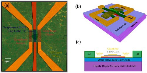
Here is (a) a general view of a scanning electron microscope (the colors in this image are artificial) (b) a 3D model and (c) a cross section of the transistor (diagram).
At the first stage of production, the WSe 2 flakes are separated by the method of mechanical exfoliation (scotch method). The graphene monolayer is manufactured by chemical vapor deposition (CVD) and is transferred to the substrate, as are several layers of boron nitride. Optical lithography and reactive ion etching is used to create the necessary pattern on the substrate. The manufacturing process is described in detail in additional materials to the article, which can be freely downloaded from the journal website.
The finished transistor exhibits outstanding electrical properties - the measured mobility of charge carriers is 45 cm 2 / (V s), which is about 100 times higher than the parameters of traditional TFT transistors.
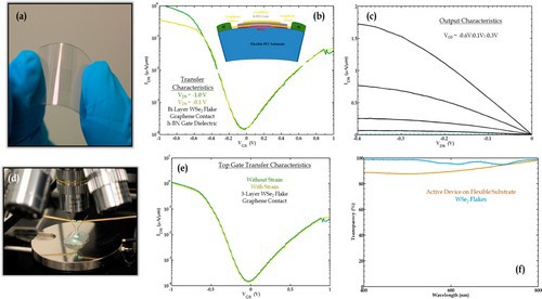 (a) Transistor on a PET substrate (be) electrical characteristics and (f) transmission spectrum in the visible range.
In addition to outstanding electrical characteristics, the transistor exhibits transparency at 88%. It retains its electrical characteristics during mechanical deformation up to 2%. All this makes it a good candidate for use in flexible electronics, especially given the recent advances in the manufacture of graphene over a large area.
')
Unfortunately, access to the original article is paid, but additional materials are available for free .
The technology allows the use of a nearly identical process for fabricating transistors on different substrates, whether they are ordinary silicon wafers or polymers such as PET. A graphene monolayer is used as electrodes. 3-4 monolayers of hexagonal boron nitride (BN) are dielectric layer, and WSe 2 bi-layer of tungsten selenide play the role of a semiconductor channel. The transistor device is shown in the following figure:
Here is (a) a general view of a scanning electron microscope (the colors in this image are artificial) (b) a 3D model and (c) a cross section of the transistor (diagram).
At the first stage of production, the WSe 2 flakes are separated by the method of mechanical exfoliation (scotch method). The graphene monolayer is manufactured by chemical vapor deposition (CVD) and is transferred to the substrate, as are several layers of boron nitride. Optical lithography and reactive ion etching is used to create the necessary pattern on the substrate. The manufacturing process is described in detail in additional materials to the article, which can be freely downloaded from the journal website.
The finished transistor exhibits outstanding electrical properties - the measured mobility of charge carriers is 45 cm 2 / (V s), which is about 100 times higher than the parameters of traditional TFT transistors.
In addition to outstanding electrical characteristics, the transistor exhibits transparency at 88%. It retains its electrical characteristics during mechanical deformation up to 2%. All this makes it a good candidate for use in flexible electronics, especially given the recent advances in the manufacture of graphene over a large area.
')
Unfortunately, access to the original article is paid, but additional materials are available for free .
Source: https://habr.com/ru/post/221415/
All Articles