STM32L-DISCOVERY + FDD
In order to connect STM32L-DISCOVERY to FDD you need 4 wires and 2 jumpers.

PS: Time is night, this is my first note on this topic, I don’t have any special knowledge, everything is described in detail on thematic resources, but I had to spend a lot of time to figure it out. Plans to make the player from the RTTTL drive.
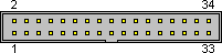
If you look at the pinout of the connector, then all the inputs / outputs are even, the odd feet are ground (GND). There must be a gap on the drive to insert the cable correctly, turn the device upside down with a gap, the upper left leg is 2.
')
Put the jumper on the 12-11 legs (“Drive Sel B” with GND) the LED on the front panel of the drive will light up, then the jumper by 16-15 (“Motor Enable B” with GND) will start the disk spinning.
From the detailed manual, we know the logical levels of TTL
Ideally, devices should have a common ground for matching logic levels, so we power the debug board directly from the drive.
The drive has a standard power connector .

Solder two wiring to the drive board (for 1 and 2 pin) and stick in EXT_5V and GND on STM32L-DISCOVERY.
Two pins, 18 DIR "Direction" and 20 STEP "Step" are used to control the drive's stepper motor.
First you need to set the direction of movement by applying LOW (0) or HIGH (1) to DIR, and then move the head by one track:
We configure the GPIO ports to output a normal logical signal, enable the clocking of the output port and 6 general-purpose timers. The tires to which they are connected can be viewed in datasheet. Further, in an endless loop, we twist the stepping motor on 100 tracks, then back and forth.
The magic number 2096 is the standard internal frequency of this controller (2.097 MHz).
Everything you need to know about Floppy Disk Drive
- Floppy Disk Drive Pinout - in great detail;
- Interfacing A Floppy Drive - here is a pseudo-code of read and write operations
- Duinomite plays the Imperial march - an example of connecting the device.
PS: Time is night, this is my first note on this topic, I don’t have any special knowledge, everything is described in detail on thematic resources, but I had to spend a lot of time to figure it out. Plans to make the player from the RTTTL drive.
Where to begin?
If you look at the pinout of the connector, then all the inputs / outputs are even, the odd feet are ground (GND). There must be a gap on the drive to insert the cable correctly, turn the device upside down with a gap, the upper left leg is 2.
')
Put the jumper on the 12-11 legs (“Drive Sel B” with GND) the LED on the front panel of the drive will light up, then the jumper by 16-15 (“Motor Enable B” with GND) will start the disk spinning.
TTL logic levels
In any case of the floppy interface used 5v TTL as the electrical interface, it would comply with LVTTL switching levels.At the outputs of the debug board, the logical unit is 3.3v, and the FDD interface uses 5v, which means that you need to connect FDD to the “5v tolerant” pins. To find them, just open the datasheet of the STM32L152RBT6 controller, which is installed on STM32L-DISCOVERY and see the table with the name "... pin definitions". If in the column “I / O structure” stands “FT” (five-volt tolerant) it means that you can safely submit 5c per pin.
From the detailed manual, we know the logical levels of TTL
An input voltage of 2.0 volts and a low voltage of 0.8 volts.This means that 3.3v is enough for us to supply a logical unit.
An output high voltage of 2.4 volts.
Ideally, devices should have a common ground for matching logic levels, so we power the debug board directly from the drive.
The drive has a standard power connector .
Solder two wiring to the drive board (for 1 and 2 pin) and stick in EXT_5V and GND on STM32L-DISCOVERY.
How to manage FDD?
Two pins, 18 DIR "Direction" and 20 STEP "Step" are used to control the drive's stepper motor.
First you need to set the direction of movement by applying LOW (0) or HIGH (1) to DIR, and then move the head by one track:
Step = LOW
Delay (1mS)
Step = HIGH
We write test firmware
Source
#include "stm32l1xx.h" #include "stm32l1xx_rcc.h" #define DIR GPIO_Pin_1 // 18 // PA1 #define STEP GPIO_Pin_2 // 20 // PA2 void delay_ms(uint32_t delay) { TIM6->PSC = 2096; TIM6->ARR = delay; TIM6->EGR |= TIM_EGR_UG; TIM6->CR1 |= TIM_CR1_CEN|TIM_CR1_OPM; while ( (TIM6->CR1 & TIM_CR1_CEN) != 0); } void InitPeriph() { GPIO_InitTypeDef GPIOConfig; GPIOConfig.GPIO_Speed = GPIO_Speed_40MHz; GPIOConfig.GPIO_Mode = GPIO_Mode_OUT; GPIOConfig.GPIO_OType = GPIO_OType_PP; GPIOConfig.GPIO_PuPd = GPIO_PuPd_NOPULL; GPIOConfig.GPIO_Pin = DIR | STEP; RCC_AHBPeriphClockCmd(RCC_AHBPeriph_GPIOA,ENABLE); GPIO_Init(GPIOA,&GPIOConfig); RCC_APB1PeriphClockCmd(RCC_APB1Periph_TIM6,ENABLE); } void move() { GPIO_ResetBits(GPIOA,STEP); delay_ms(1); GPIO_SetBits(GPIOA,STEP); } int main() { int i; InitPeriph(); for(;;) { GPIO_ResetBits(GPIOA,DIR); for(i=0;i<100;i++) { move(); } delay_ms(1000); GPIO_SetBits(GPIOA,DIR); for(i=0;i<100;i++) { move(); } delay_ms(2500); } } We configure the GPIO ports to output a normal logical signal, enable the clocking of the output port and 6 general-purpose timers. The tires to which they are connected can be viewed in datasheet. Further, in an endless loop, we twist the stepping motor on 100 tracks, then back and forth.
The magic number 2096 is the standard internal frequency of this controller (2.097 MHz).
Source: https://habr.com/ru/post/221023/
All Articles