Scientists from IBM have discovered an interesting physical phenomenon on the example of "nanowires" of semiconductors
In our time, miniaturization is one of the main factors driving technical progress. In fact, nowadays in computer technology conductors are used, the thickness of which is thousands of times smaller than the thickness of a human hair. Thanks to the vanishingly small size, it becomes possible to create powerful, productive chips of small sizes, capable of doing what the computing nodes of previous years, which occupied whole rooms, were not capable of doing.
Now actively developing data transmission technology using light signals, within a single chip. This is possible due to the combination of optical elements with semiconductors, graphene and carbon nanotubes, when the entire system is placed on a silicon substrate.
')
Data transmission using such a system usually means the need to convert electrical signals into light signals, and vice versa. For the conversion of the first type materials are usually used III-V groups of semiconductors that emit light. Well, for the reverse transformation, light into electricity uses silicon and germanium.
A team of IBM scientists discovered an interesting physical phenomenon, which can lead to the fact that in the future the same material will be used both to emit light and to convert it into electricity, within the same chip.
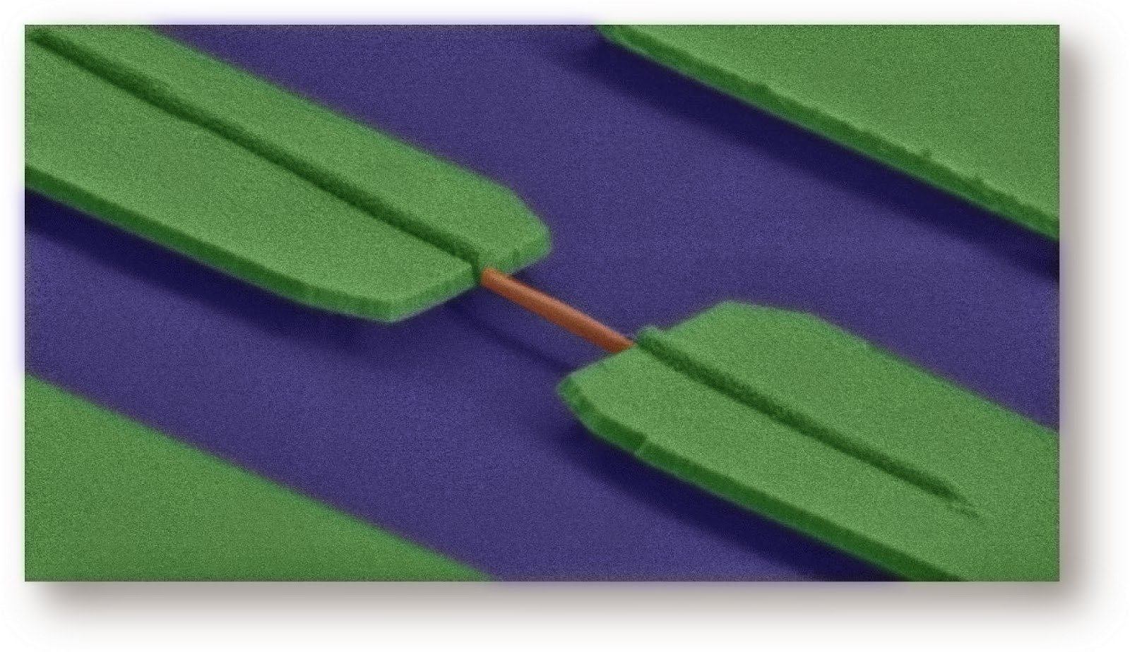
The journal Nature Communications recently published an article by scientists from Zurich's IBM Research division. The article talked about the fact that "nanowires" of a semiconductor can serve as an effective light emitters, and effective photodetectors. And to switch a substance from the state of "radiation" to the state of "detection" you need mechanical stress.
“When you stretch the nanowire along its entire length, the material goes into a state that we call the“ forbidden zone with a direct transition ”(direct bandgap), in which it effectively emits light. But when you compress the conductor along the axis, its electronic properties change, the material stops emitting light. We call this state “pseudo-direct zone” (pseudo-direct), in this state, materials of group III-V behave like germanium or silicon, and become good photo-detectors, ”one of the researchers, Giorgio Signorello, comments on the discovery.
“These unusual properties are due to the fact that atoms are very specific located in such a conductor. We call this crystal structure "Wurtzite". The implementation of such a structure is possible only due to the ultra-small size of the nanowire. You will not be able to achieve the same material properties with the size visible to the eye. This is an excellent example of the power of nanotechnology, ”says a colleague of the first scientist, Heike Riel.
As mentioned above, a similar phenomenon can open the possibility of creating devices for optical data transmission, where the same material is used both for emitting light and for detecting it.
And this means new achievements, new breakthroughs in this area.
Via rdmag + ibmresearchnews
Source: https://habr.com/ru/post/220451/
All Articles