This is Science: Silicon electronics: bend me completely
Today, it seems that modern electronics is something solid, solid, but the day and hour when electronic devices become flexible (and some manufacturers have already succeeded!) Is near, smart phones can be turned into a tube, and a 2 meter monitor will be automatically "Roll out" when you turn on the TV or computer ... This, of course, is still a dream, but the real flexible electronics are already produced in laboratories around the world as prototypes for finding the most optimal and cheap technology.
')
The topic of creating flexible non-carbon electronics, namely silicon electronics, prompted developers from the King Abdullah Institute of Science and Technology, which in Saudi Arabia (yes, oil is not a hindrance to progress), to develop a new method for transferring microelectronic components such as capacitors, transistors, and whole microchips on a flexible substrate of silicon dioxide or polycrystalline / amorphous silicon.
Of course, the solution of this issue is not new, and many laboratories have already done a lot of work in this field. For example, IBM a year ago presented its vision of flexible electronics, before that many attempts were made to create “spring-loaded” contacts , to fasten separate small chips on ordinary silicon with conductive polymers, and even a solution based on carbon nanotubes , but the technology described below requires only a small amount changes in process technology in production and uses silicon and silicon dioxide.
So, few probably know that ordinary glass can be bent almost in half, the whole thing only in the thickness of the product. This is actually the same thing as comparing aluminum or iron thin foil with a bulky piece of metal. Here and the presented technology uses this effect, that is, the thickness of the substrate is reduced to only 5 microns. In order to separate the substrate from the carrier, holes are drilled in it about 3-5 micrometers in size, through which then the reaction etching takes place with a uniform separation of the substrate of the carrier.
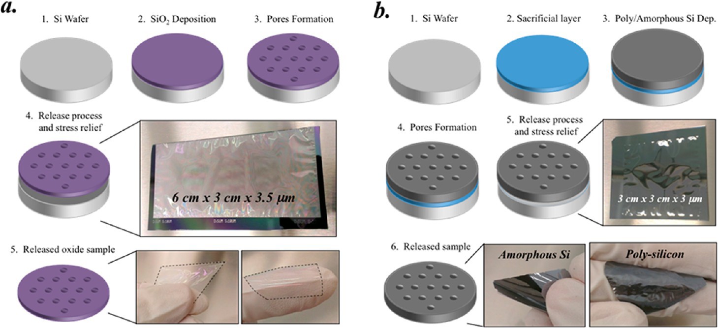
Two processes for creating flexible electronics: a) on a transparent silicon dioxide substrate and b) on a conventional silicon substrate
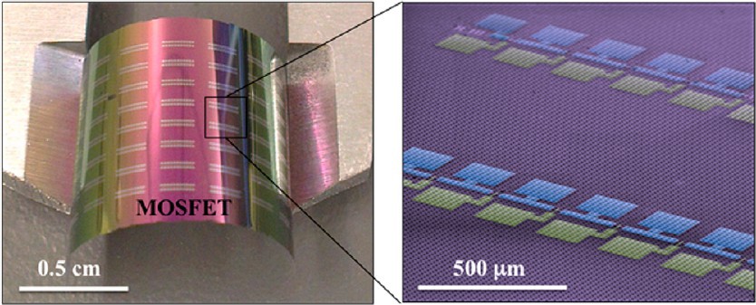
To test the operability and reproducibility of this technological process, the authors of the work created flexible semiconductor capacitances (MOSCAP), field-effect transistors ( MOSFET ), and metal-insulator-metal capacitors (MIMCAP). All test samples confidently bend and demonstrate almost indistinguishable characteristics in comparison with the bulk counterparts.
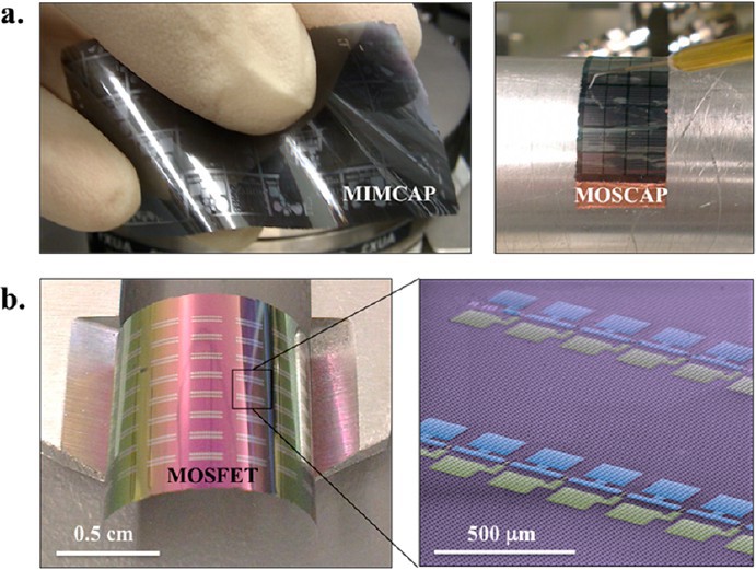
Capacitors and field-effect transistors created on a thin and flexible silicon plate
But that's not all, the work also presents the work of ready-made devices such as a micro-Li-Ion battery and a thermoelectric generator:

Demonstration of the operation of real devices: ab) thermoelectric generator and its characteristics ©, d) lithium battery and its capacity (e)
Speaking of cost, the authors write that all the processes involved in manufacturing are equivalent to those used in conventional production, with the exception of one — reactive etching with XeF 2 followed by separation of the plate. However, about 2 g of this compound is consumed per 18 cm 2 plate (100 cycles, 30 s / cycle). Taking into account the cost of $ 8 / g, it turns out that the whole etching procedure goes to 0.88 $ / cm 2 , which is not so little. A recovery of Xe - at least partial - will reduce costs many times. In addition, thinning the substrate will significantly save materials.
And finally, a video in which the authors “play” with a 4 inch plate, which can be taken here .
The original article was published in ACSNano magazine.
Sometimes briefly, and sometimes not so much about the news of science and technology, you can read on my Telegram channel - welcome;)
Source: https://habr.com/ru/post/219211/
All Articles