Have you seen your printed circuit boards under the microscope?
I make printed circuit boards by myself, LUT.
The first stage is the transfer of the picture. After - check the quality of the transfer of toner to the board. If all is well - we hate. Somewhere the track fell off, the landfill badly stuck - it does not matter, the marker in hand and forward. Corroded? Inspect the board for the integrity of tracks / heels / polygons / different characters, etc.
Looking at my brainchild once again, it dawned on me: “What if you look at the board through a microscope?” A break in the conductor, of course, I will notice, but it's interesting to look at the smallest details: the edges of the tracks, the middle of the holes. (Caution - a lot of photos!)
So, let's begin.
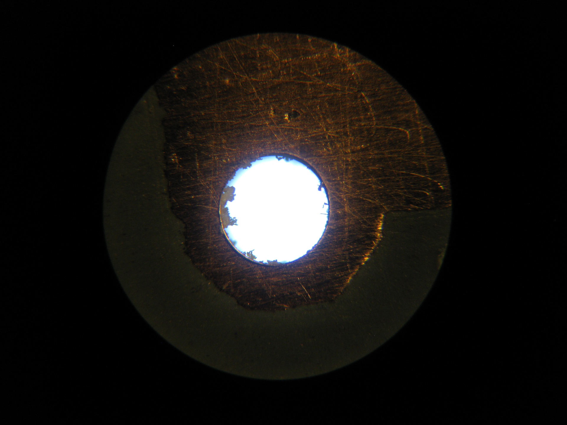
1. The entire board, just etched, on the microscope stage:

The holes for the components have not been drilled yet.
')
2. Platform for smd component:

It is evident that the toner has already begun to depart. Fortunately, this did not happen during etching.
3. Another playground, but already for the terminal part:

Toner, too, is not all present.
4. And here comes the chip. Toner peeling, but almost perfect track is visible under it:

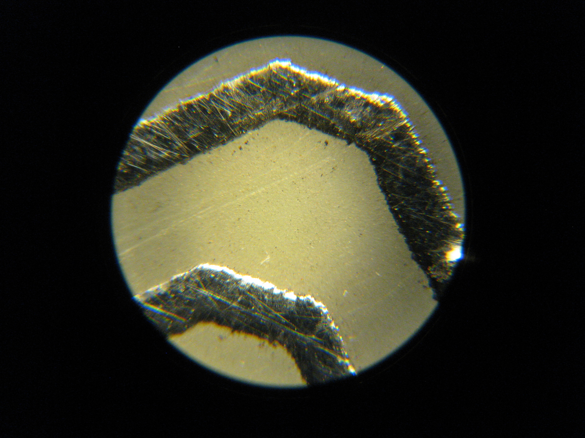
5. Oval playground. Apparently, the toner on it did not fit very well on the board, as a result, the required copper partially “left”.

6. Tracks. With a width of 0.4 turned out pretty good.

7. Remember, I said that in the right places the board can be tinted with a marker?


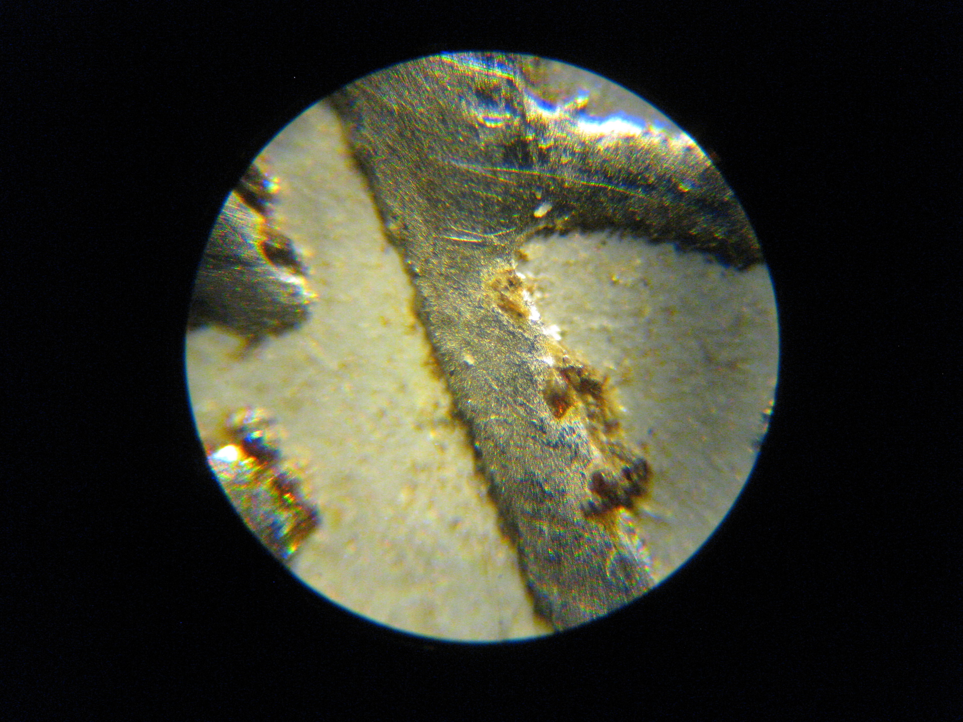
8. This track FeCl 3 not spared:

9. The edges of the polygons are not always smooth:

10. Here too much has become tooiled:

11. Noticed a small eight next to the place under the chip?

12. Pad for hatcher:

13. Unidentified item on the board:

The photo was not very good, because so very small is something.
14. Drilled holes, sanded:


15. Cleared tracks:

16. Pad with a hole. It can be seen as the drill broke the reverse side of the board:
17. Letters on the board. Notice how much shavings are around:

18. Everything! The fee is tinned (the tracks are the same, from №6):
19. Indelible flux between tracks and letters:

No wonder, apparently, advised to wash it.
20. Tinned Eight:

21. More tinned components:


As you can see, even not very smooth and etched parts are well tampered and now look neat.
22. And finally. Board edge:

Now you understand why they are advised to clean / dub?
For the sim - everything. Thanks for attention.
ZY This is not the most worthy representatives of LUT technology. With a laser iron, having gotten in, you can make tracks 0.1 mm wide. What makes LUT so attractive to me is:
There is, of course, this technology and its drawbacks. I will not write about them anymore, I think everyone knows them himself.
One more photo:


LUT on magazine paper. The board is made from the first time. It took ~ 5 minutes to transfer the pattern and strip the board (the time for heating the iron is also taken into account). Track 0.254 mm, a distance of 0.4096 mm. Of course, there are drawbacks, but such boards will work. When manufacturing speed is important - IMHO, the most suitable way.
The first stage is the transfer of the picture. After - check the quality of the transfer of toner to the board. If all is well - we hate. Somewhere the track fell off, the landfill badly stuck - it does not matter, the marker in hand and forward. Corroded? Inspect the board for the integrity of tracks / heels / polygons / different characters, etc.
Looking at my brainchild once again, it dawned on me: “What if you look at the board through a microscope?” A break in the conductor, of course, I will notice, but it's interesting to look at the smallest details: the edges of the tracks, the middle of the holes. (Caution - a lot of photos!)
So, let's begin.
1. The entire board, just etched, on the microscope stage:
The holes for the components have not been drilled yet.
')
2. Platform for smd component:
It is evident that the toner has already begun to depart. Fortunately, this did not happen during etching.
3. Another playground, but already for the terminal part:
Toner, too, is not all present.
4. And here comes the chip. Toner peeling, but almost perfect track is visible under it:
5. Oval playground. Apparently, the toner on it did not fit very well on the board, as a result, the required copper partially “left”.
6. Tracks. With a width of 0.4 turned out pretty good.
7. Remember, I said that in the right places the board can be tinted with a marker?
8. This track FeCl 3 not spared:
9. The edges of the polygons are not always smooth:
10. Here too much has become tooiled:
11. Noticed a small eight next to the place under the chip?
12. Pad for hatcher:
13. Unidentified item on the board:
The photo was not very good, because so very small is something.
14. Drilled holes, sanded:
15. Cleared tracks:
16. Pad with a hole. It can be seen as the drill broke the reverse side of the board:
17. Letters on the board. Notice how much shavings are around:
18. Everything! The fee is tinned (the tracks are the same, from №6):
19. Indelible flux between tracks and letters:
No wonder, apparently, advised to wash it.
20. Tinned Eight:
21. More tinned components:
As you can see, even not very smooth and etched parts are well tampered and now look neat.
22. And finally. Board edge:
Now you understand why they are advised to clean / dub?
For the sim - everything. Thanks for attention.
ZY This is not the most worthy representatives of LUT technology. With a laser iron, having gotten in, you can make tracks 0.1 mm wide. What makes LUT so attractive to me is:
- board manufacturing speed;
- cost, in comparison with photoresist (materials are cheaper);
- the opportunity to work less with chemistry.
There is, of course, this technology and its drawbacks. I will not write about them anymore, I think everyone knows them himself.
One more photo:
LUT on magazine paper. The board is made from the first time. It took ~ 5 minutes to transfer the pattern and strip the board (the time for heating the iron is also taken into account). Track 0.254 mm, a distance of 0.4096 mm. Of course, there are drawbacks, but such boards will work. When manufacturing speed is important - IMHO, the most suitable way.
Source: https://habr.com/ru/post/218765/
All Articles