Smart watch do it yourself for 1500 rubles. Part 2 - Board and Components
Due to numerous requests, I post the source of the clock scheme with a description of the components.
The circuit and the board were made in the DipTrace program.
When I ordered components for watches, there was a slightly different set, but due to the lack of those models that I wanted, I had to take these:


')


Charging current is regulated by a resistor according to the formula:

Since The battery charge current is 100mA, then the resistor is 10kOhm.


Taken from here
The lever for controlling the clock was taken from the old communicator. It has 3 positions: up, center, bottom. Also, just in case, the reset button MK is added. Vibrating motor from the same communicator. Quartz for CRR from the Launchpad set. The miniUSB port is taken from the broken card reader. LED for charging status indication I don’t remember where it’s coming from =)
It remains to connect all the blocks together and see what happens.
Yeah, between the battery and the ground, there are 2 capacitors for 1uF (stabilizer) and 4.7uF (charging). We take only the larger one at 4.7uF. Yes, and between 5V from USB and ground again there are 2 capacitors for 1uF (USB-UART) and 4.7uF (charging). Again we take only the larger one at 4.7uF.
Scheme in the studio!

To save power, the BT power must be turned off when not in use. To do this, let's get a power pin on the MK leg. But! In this state, BT did not start. As far as I remember, the load on each pin is limited to 40mA and apparently this is not enough to turn on the BT. Therefore, we connect the power BT to two pins. (of course, it would be possible to make a power key on transistors, but this is extra space on the board for components + complication of the circuit, etc.).
Just want to know when BT is connected, and when waiting for a connection. To do this, let's get the BT LED pin on the MK pin. When enabled without connecting to this pin log. sequence 01010101 ... In the connected state there is always a log on it. one.
To measure the voltage on the battery, a voltage divider with two resistors was connected to the ADC input. The values of the resistors were chosen so that the input to the ADC when charging (maximum voltage 4.25V) was less than 3.3V.
The voltage regulator outputs 3.28 - 3.29 volts with an input voltage of more than 3.4 and about 0.1 - 0.2 volts less than the input when the input is from 2.7 to 3.3 volts. And when the input is less than 2.7 is disabled.
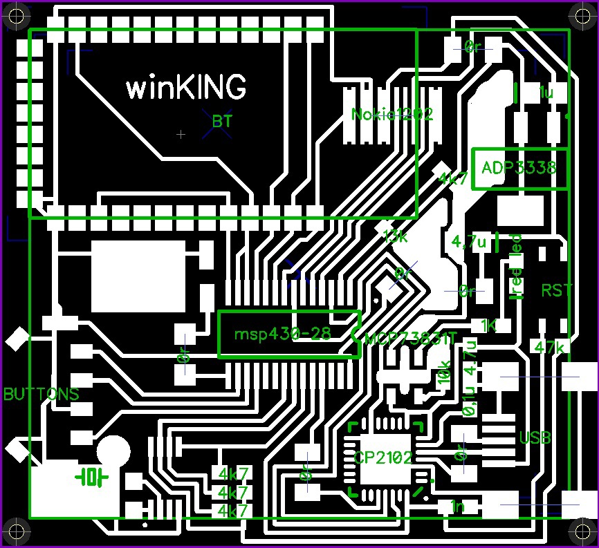
The layout of the board was made manually. Initially, there were only a few pins of the MC to which it was necessary to connect external components, namely:
First, all components were placed on the board. Then there was a connection for the above points. Then the layout of all other components.
The bottom right 5 pins of the BT should be isolated from the board. Quartz is soldered to the substrate connected to the ground. For convenience of soldering, near the first pins of the microcircuits, dots are put.
Source codes and boards here
That seems to be all. As always, I look forward to questions and comments.
Part 1 - Start
The circuit and the board were made in the DipTrace program.
When I ordered components for watches, there was a slightly different set, but due to the lack of those models that I wanted, I had to take these:
Stabilizer:
- Model: ADP3338AKCZ-3.3-RL7;
- body: SOT-223;
- input voltage: 2.7V - 8V;
- output voltage 3.3V;
- maximum load: 1A (picked up with a margin);
- Maximum own consumption in Regulation mode: 3mA at 100mA load, 0.19mA at 0.1mA load; in Dropout mode :, 0.6mA at 0.1mA load;
- connection diagram:
Real time clock:
- Model: DS1337U +;
- case: 8 uSOP;
- input voltage: 1.8V - 5.5V;
- maximum consumption: 0.15mA (if you look at the graph, at an input voltage of 3.3V, consumption ~ 40uA);

- interface protocol: I2C;
- connection diagram:
')
Bluetooth:
- Model: HC-06;
- body: your;
- input voltage: 3.0V - 4.2V;
- maximum consumption before connection: fluctuations in the range of 30-40 mA (~ 25mA), after connection: 8mA;
- connection diagram:
Battery:
- Model: LIR3048;
- body: your;
- output "normal" voltage: 3.6V;
- "Normal" capacity: 200mAh;
- charging voltage: 4.25V;
- charge current: “normal” 0.5C (100mA), max. 1C (200mA);
- maximum discharge current: 2C (400mA);
Battery Charging Controller:
- Model: MCP73831T_2ACI_OT;
- body: SOT-23-5;
- input voltage: 3.75V - 6V;
- consumption is not interested;
- connection diagram:
Charging current is regulated by a resistor according to the formula:
Since The battery charge current is 100mA, then the resistor is 10kOhm.
USB - UART:
- Model: CP2102-GMR;
- housing: MLP-28;
- input voltage: 4V - 5.25V;
- consumption is not interested;
- connection diagram:
Microcontroller:
- Model: msp430g2553ipw28;
- housing: TSSOP28;
- input voltage: 1.8V - 3.6V;
- consumption: depends on the power consumption mode, the included modules, the processor frequency, etc .;
- pin connections: A 47kOhm pull-up resistor and a 10nF capacitor to ground (no more than 2.2nF when using the SBW or JTAG interface);
Screen:
- model: nokia 1202;
- body: your;
- input voltage: 3.3V;
- connection diagram:
Taken from here
Rest:
The lever for controlling the clock was taken from the old communicator. It has 3 positions: up, center, bottom. Also, just in case, the reset button MK is added. Vibrating motor from the same communicator. Quartz for CRR from the Launchpad set. The miniUSB port is taken from the broken card reader. LED for charging status indication I don’t remember where it’s coming from =)
Scheme
It remains to connect all the blocks together and see what happens.
Yeah, between the battery and the ground, there are 2 capacitors for 1uF (stabilizer) and 4.7uF (charging). We take only the larger one at 4.7uF. Yes, and between 5V from USB and ground again there are 2 capacitors for 1uF (USB-UART) and 4.7uF (charging). Again we take only the larger one at 4.7uF.
Scheme in the studio!
To save power, the BT power must be turned off when not in use. To do this, let's get a power pin on the MK leg. But! In this state, BT did not start. As far as I remember, the load on each pin is limited to 40mA and apparently this is not enough to turn on the BT. Therefore, we connect the power BT to two pins. (of course, it would be possible to make a power key on transistors, but this is extra space on the board for components + complication of the circuit, etc.).
Just want to know when BT is connected, and when waiting for a connection. To do this, let's get the BT LED pin on the MK pin. When enabled without connecting to this pin log. sequence 01010101 ... In the connected state there is always a log on it. one.
To measure the voltage on the battery, a voltage divider with two resistors was connected to the ADC input. The values of the resistors were chosen so that the input to the ADC when charging (maximum voltage 4.25V) was less than 3.3V.
The voltage regulator outputs 3.28 - 3.29 volts with an input voltage of more than 3.4 and about 0.1 - 0.2 volts less than the input when the input is from 2.7 to 3.3 volts. And when the input is less than 2.7 is disabled.
PCB layout
The layout of the board was made manually. Initially, there were only a few pins of the MC to which it was necessary to connect external components, namely:
- I2C interface: pins P1.7 (SDA) and P1.6 (SCL);
- USB - UART for flashing: pins TEST, RST, P1.1 (TX) and P1.5 (RX);
- voltage divider: any ADC input (P1.x).
First, all components were placed on the board. Then there was a connection for the above points. Then the layout of all other components.
The bottom right 5 pins of the BT should be isolated from the board. Quartz is soldered to the substrate connected to the ground. For convenience of soldering, near the first pins of the microcircuits, dots are put.
Source codes and boards here
That seems to be all. As always, I look forward to questions and comments.
Part 1 - Start
Source: https://habr.com/ru/post/218645/
All Articles