Korean scientists have developed a revolutionary technology for the production of graphene
Although graphene consists of carbon that is widespread in nature, it is very expensive, since methods of its production on an industrial scale have not yet been invented. It is relatively easy to get only the smallest graphene flakes. A large single-layer sheet of single-crystal graphene, suitable for further use in microelectronics, is an unattainable goal for the time being.
However, it seems that a breakthrough is not far off. Just a few months ago, at the Thomas Watson IBM Research Center, they learned how to get 10 cm sheets of graphene . And on April 3 of this year, the journal Science published the results of a joint study of scientists from the Institute of Advanced Technologies Samsung and Songjungwan University (South Korea), which describes another method of obtaining large sheets of graphene with an ideal structure, potentially suitable for mass production.
The main problem of growing graphene is the presence of regions with different orientations of the crystal lattice, at the joints of which defects are formed. This problem could have been avoided if we grow a large sheet of graphene from a single crystallization center, but this is very difficult to put into practice. Korean scientists have found a way to carry out the crystallization of graphene so that all areas in which crystallization began, were oriented the same way and coalesced into a coherent whole without defects. A key element of the new technology is a specially treated substrate.
')
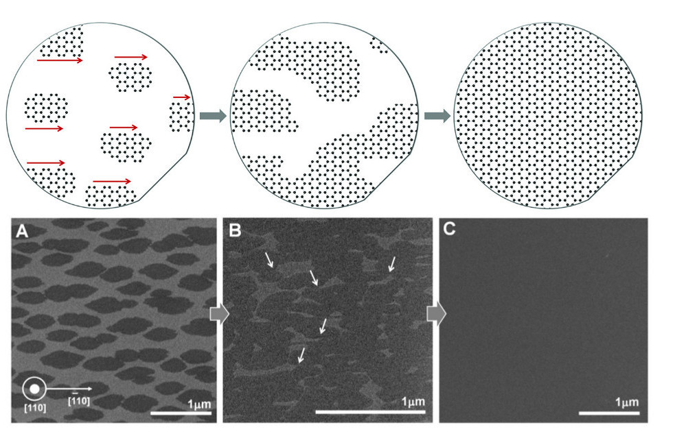
Separate areas of graphene grow together into a single sheet (at the top - a diagram, at the bottom - images from a microscope)
It is based on a conventional silicon wafer used for the production of microchips. It is covered with a thin layer of monocrystalline germanium, and then its surface is treated with a 10% aqueous solution of hydrogen fluoride (hydrofluoric acid). The acid dissolves the oxide film on the surface of germanium and instead forms a layer of hydrogen atoms. Such a substrate has two very important properties.
First, the germanium crystal lattice serves as a kind of template for deposited carbon atoms — all crystallization centers are oriented equally, and subsequently coalesce ideally. Secondly, it has low adhesion with graphene - this makes it easy to smooth out folds formed at the junction of different areas of graphene or due to differences in the coefficient of thermal expansion of graphene and germanium. Low adhesion also makes it easy to separate a sheet of graphene from the substrate without damaging it. In many other ways of producing graphene, the substrate has to be dissolved. This makes production unprofitable, since the creation of a perfectly flat and clean substrate is in itself expensive.
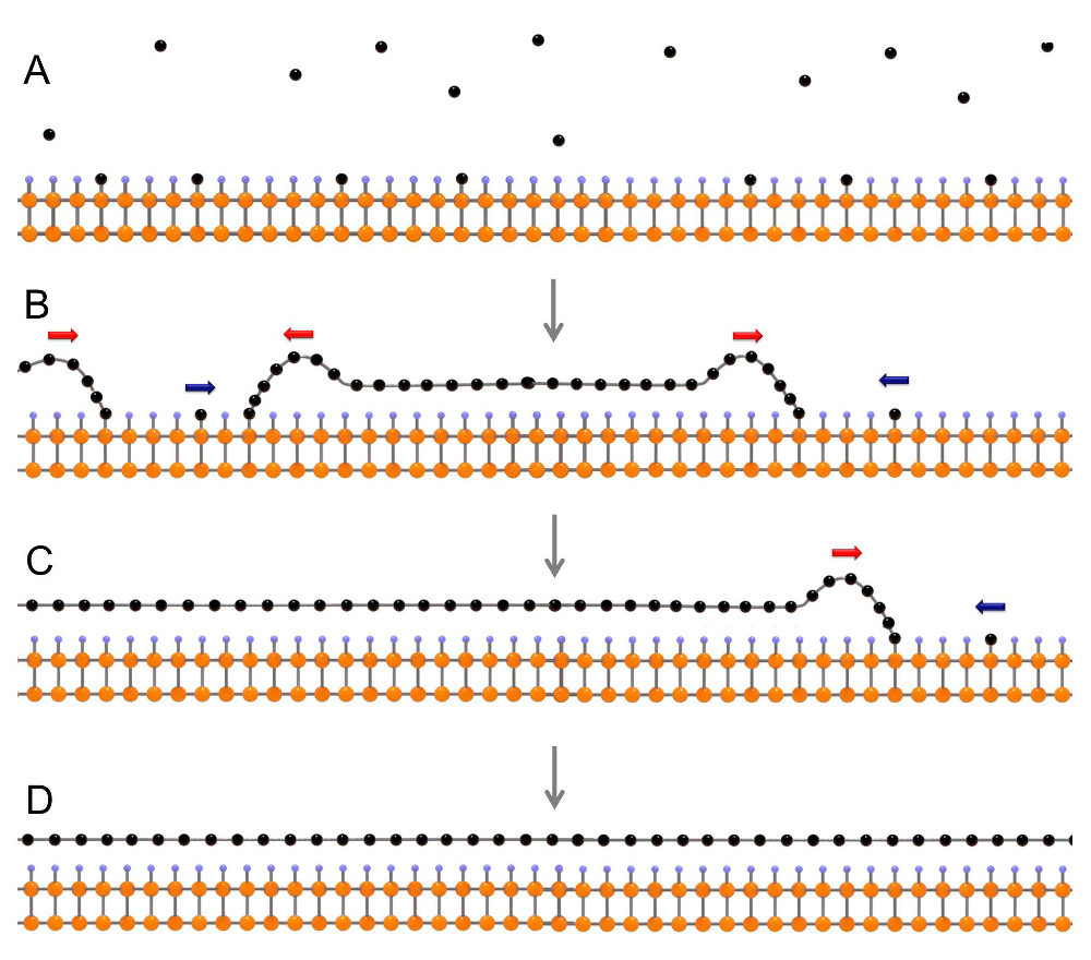
A) Start of carbon deposition; B) the formation of individual areas of graphene; C) the regions grow together; D) finished graphene sheet. Carbon atoms are black, germanium is orange, hydrogen is blue.
The source of carbon atoms is methane. Deposition of carbon on the substrate occurs at a temperature of 900 - 930 degrees Celsius and a pressure of about 13% atmospheric for a time from 5 to 120 minutes. Electron microscopy confirmed the absence of defects and irregularities in the structure of a graphene sheet. From the graphene thus synthesized, scientists have successfully manufactured a field-effect transistor. Employees of the Samsung laboratory said that the developed technology is "one of the most significant breakthroughs in the history of graphene research." They believe that this discovery will significantly accelerate the industrial development of graphene and open a new era in electronics.
However, it seems that a breakthrough is not far off. Just a few months ago, at the Thomas Watson IBM Research Center, they learned how to get 10 cm sheets of graphene . And on April 3 of this year, the journal Science published the results of a joint study of scientists from the Institute of Advanced Technologies Samsung and Songjungwan University (South Korea), which describes another method of obtaining large sheets of graphene with an ideal structure, potentially suitable for mass production.
The main problem of growing graphene is the presence of regions with different orientations of the crystal lattice, at the joints of which defects are formed. This problem could have been avoided if we grow a large sheet of graphene from a single crystallization center, but this is very difficult to put into practice. Korean scientists have found a way to carry out the crystallization of graphene so that all areas in which crystallization began, were oriented the same way and coalesced into a coherent whole without defects. A key element of the new technology is a specially treated substrate.
')
Separate areas of graphene grow together into a single sheet (at the top - a diagram, at the bottom - images from a microscope)
It is based on a conventional silicon wafer used for the production of microchips. It is covered with a thin layer of monocrystalline germanium, and then its surface is treated with a 10% aqueous solution of hydrogen fluoride (hydrofluoric acid). The acid dissolves the oxide film on the surface of germanium and instead forms a layer of hydrogen atoms. Such a substrate has two very important properties.
First, the germanium crystal lattice serves as a kind of template for deposited carbon atoms — all crystallization centers are oriented equally, and subsequently coalesce ideally. Secondly, it has low adhesion with graphene - this makes it easy to smooth out folds formed at the junction of different areas of graphene or due to differences in the coefficient of thermal expansion of graphene and germanium. Low adhesion also makes it easy to separate a sheet of graphene from the substrate without damaging it. In many other ways of producing graphene, the substrate has to be dissolved. This makes production unprofitable, since the creation of a perfectly flat and clean substrate is in itself expensive.
A) Start of carbon deposition; B) the formation of individual areas of graphene; C) the regions grow together; D) finished graphene sheet. Carbon atoms are black, germanium is orange, hydrogen is blue.
The source of carbon atoms is methane. Deposition of carbon on the substrate occurs at a temperature of 900 - 930 degrees Celsius and a pressure of about 13% atmospheric for a time from 5 to 120 minutes. Electron microscopy confirmed the absence of defects and irregularities in the structure of a graphene sheet. From the graphene thus synthesized, scientists have successfully manufactured a field-effect transistor. Employees of the Samsung laboratory said that the developed technology is "one of the most significant breakthroughs in the history of graphene research." They believe that this discovery will significantly accelerate the industrial development of graphene and open a new era in electronics.
Source: https://habr.com/ru/post/218357/
All Articles