JTAG Peripheral Scanning: Testing Electronics Prototypes
In this article, we will share practical experience in the use of peripheral (boundary) JTAG scanning and describe the features and benefits of introducing this technology at the stage of testing prototypes. Special attention will be paid to typical errors detected by JTAG using the Provision software package for testing various nodes and microcircuits of the board.
Recall that a peripheral scan (boundary scan) is a structural test of a printed circuit board with installed components, which is based on the application of IEEE 1149.x standards. The result of the scan is information on the presence in the electrical circuits of typical faults that occur during the production of printed circuit boards: short circuits (bridges), non-interruptions (opens), dropping to 0 or 1 (stuck at 0, stuck at 1), breaks in the tracks.
')
JTAG testing will be performed on the board that came from production.
JTAG testing allows you to detect non-solder in BGA packages, closures, breaks, as well as non-working chips with digital interfaces. Identifying these defects is very important, because if an untested board falls into the hands of a programmer, problems start up with running memory and other peripherals. It is often not clear what the reason is: in the wrong settings that the programmer makes, or in the editing defect . JTAG testing can identify these problems.
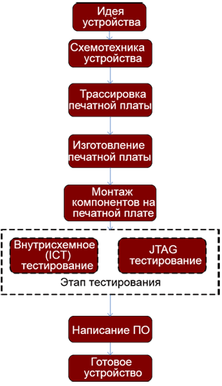
At the testing stage (before the first power up), the absence of a short circuit on the boards is checked. Next, the supply voltage is applied and the current consumption is checked, then the main supply voltages are checked. Then the board undergoes either JTAG or intracircuit (ICT) testing (alternatively, you can use two tests in turn).
Since JTAG is the very first test, the problems it has identified save labor costs in the future . It is logical that if problems are detected after the assembly of the device, it will have to be disassembled and reassembled.
At the stage of JTAG testing revealed:
- not soldered on microcircuits with BGA packages, for which ICT testing cannot be implemented in principle;
- unplugged pull-up / down resistors;
- tie-in short circuit.
Also, with the help of JTAG technology, memory chips are successfully tested: from SRAM to DDR3 (only the correctness of the mounting of the circuits is analyzed, not the memory itself). This test in conjunction with the flash-memory test allows you to pay a fee to the programmer to install the initial bootloader, the OS, and the subsequent Bringup (first run).
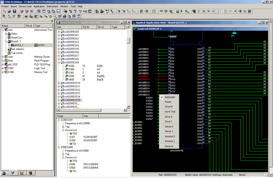
Using JTAG tests on Provision software as an example for functional testing of printed circuit boards
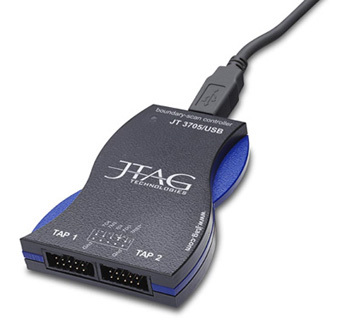
The software package Provision for conducting JTAG testing allows you to generate automated tests, includes an extensive library of models for testing chips, has a good technical. support and friendly interface.
We used Provision for testing in projects with a miniature element base, housings 0402 and BGA, high-density layout, more than 4 layers of boards and flexible-rigid boards.
Consider the use of technology boundary scanning on specific projects:
Example number 1. VoIP router
Task: to develop a device for VoIP-telephony based on a Blackfin BF527 processor with software based on Linux OC.

In this project, SDRAM, NAND, Ethernet switch chips were tested. Also, JTAG checked the correctness of the LEDs and buttons - for this, functional tests written in the Python language were used. This is a scripting language integrated into Provision. With it, you can test various digital interfaces and chips, as well as organize a flexible dialogue with the user.
The use of JTAG-testing allowed to check the correctness of the installation and operation of the chips.
Example number 2. Plug computer
Objective: to develop a multi-functional network device ( mini-server ), designed to work in IP-based networks.
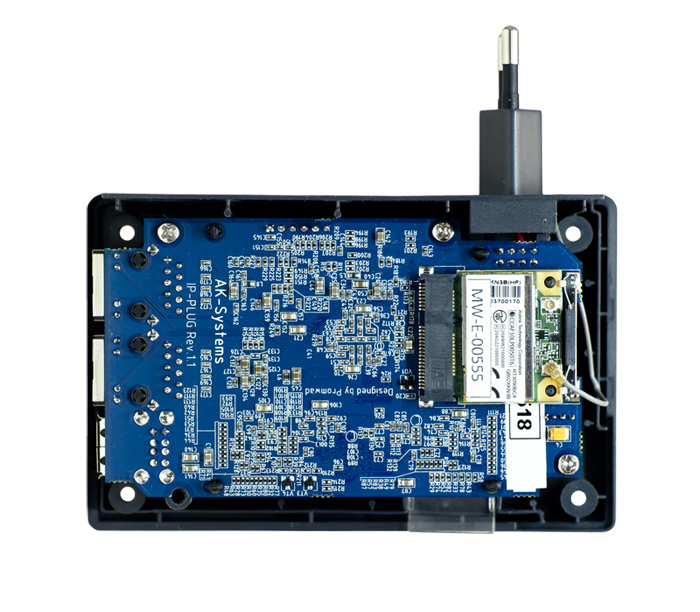
This project uses a 88F6282 processor from Marvell and DDR2 / DDR3 memory. On the board of limited sizes, double-sided mounting and 7 microcircuits with BGA packages are used. During the recovery of the boards, there were problems with the memory, they manifested themselves in the form of hang-ups of the boards during boot-up or the inability to start the U-boot. Operational tests of DDR2 memory were carried out, which revealed non-soldered outputs on the data bus on the D0, D3, D7 lines of one of the 4 memory chips. Because of this defect, the data in a specific address space spontaneously changed.
In versions of a device with DDR3 memory, programmers had problems loading Linux. It was decided to promptly check the quality of the installation of these chips. As a result of testing, it turned out that all the chips were in good order, and the problem lay in incorrectly set timings.
As a result, JTAG testing helped save considerable time at the bringup stage, since by transferring the board to programmers, it was safe to say that the memory was well-sealed.
During this project, the responsiveness of technical support from JTAG Technologies was evaluated.
Example number 3. JADE processor module on Fujitsu JADE chip
Objective: to develop an on-board computer to control, monitor and diagnose auxiliary equipment of trucks and special vehicles.
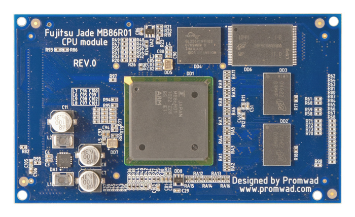
This project is a dual-board processor module and a motherboard (in the photo, only the module itself). Emphasis was placed on testing the connections between the boards, a test was also carried out to verify the generation of generators, the correctness of mounting NAND and NOR memory.
During the testing of prototype devices, the absence of generation was revealed at one of the conclusions. A visual inspection revealed that during the installation the key was mixed up on the generator.
Example number 4. Single board industrial computer
Task: development of the SOM01 processor board based on the TI AM1808 processor (ARM926, 456MHz).
This device is a single board computer implemented in the SO-DIMM 200 form factor. During the implementation of this project, a detailed DFT analysis was made, the coverage was determined and steps were recommended for increasing the test coverage. For maximum coverage of the board with JTAG tests, a stand was designed that increased coverage to 98% (only the USB interface was uncovered, since the TAP controller does not have access to these findings). Also, this stand allows you to flash the board via Uart or Ethernet, control voltages and currents.
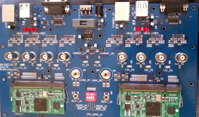
In the photo: a test stand with connected boards
findings
The JTAG border scanning technology can be successfully applied in production to control the correctness of installation, to test prototypes, and to manufacture the series.
To implement this technology into production, you must purchase a software package and a hardware adapter. To test a specific board, a set of scripts written in this environment is needed.
The advantages of JTAG testing over ICT testing is that there is no need to place additional contact pads for an ICT tester (in more detail we already wrote about this in the article “How to test electronics in production: analysis of modern technologies” ).
Also, using JTAG testing, you can test the correctness of mounting BGA packages, which is not possible with in-circuit testing.
As a result, JTAG technology can significantly reduce the time of the bingap of prototypes. The developer of the device independently writes tests in a scripting language, taking into account all the nuances of the work of each specific scheme.
Thanks for attention. Questions and comments are welcome.
Source: https://habr.com/ru/post/216411/
All Articles