New Brief: Samsung starts mass production of 4 Gbps DDR3 mobile memory chips
Good afternoon, Habr!
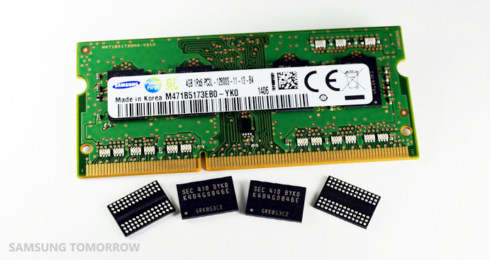
Yesterday, Samsung announced the start of mass production of 20-nanometer DDR3 memory chips with a density of 4 Gbps. The release of this DRAM-memory, each cell of which consists of an associated transistor and a capacitor, is much more complicated than the production of NAND-type flash memory with a single transistor; therefore, traditionally the volumes of DRAM chips are noticeably inferior to those of flash memory chips.
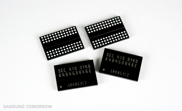
To cope with this difficult task, Samsung experts have combined a modified technology of exposure with a double pattern and atomic layer deposition technology. This not only allowed the company to produce DDR3 memory chips using the 20-nm process technology using existing immersion ArF-lithography (lithography using argon fluoride excimer lasers operating in the hard ultraviolet range), but also make it possible to manufacture next-generation DRAM technology class 10 nm in the near future.
')

In addition, Samsung has achieved an unprecedented uniformity of deposition of ultra-thin dielectric capacitor layers, which further improved the memory efficiency. At the same time, the company managed to increase production efficiency: for new chips, it is 30% higher than for DDR3 using the 25-nm process technology, and twice as much as DDR3 using the 30-nm process technology. The energy efficiency indicators of the chips are 25% ahead of the characteristics of the mobile memory manufactured using the 25-nm process technology. This achievement will be the basis for the development of the latest "green" IT solutions for global companies.
According to Gartner's research, the global mobile memory market will increase from $ 35.6 billion in 2013 to $ 37.9 billion in 2014.
Yesterday, Samsung announced the start of mass production of 20-nanometer DDR3 memory chips with a density of 4 Gbps. The release of this DRAM-memory, each cell of which consists of an associated transistor and a capacitor, is much more complicated than the production of NAND-type flash memory with a single transistor; therefore, traditionally the volumes of DRAM chips are noticeably inferior to those of flash memory chips.
To cope with this difficult task, Samsung experts have combined a modified technology of exposure with a double pattern and atomic layer deposition technology. This not only allowed the company to produce DDR3 memory chips using the 20-nm process technology using existing immersion ArF-lithography (lithography using argon fluoride excimer lasers operating in the hard ultraviolet range), but also make it possible to manufacture next-generation DRAM technology class 10 nm in the near future.
')
In addition, Samsung has achieved an unprecedented uniformity of deposition of ultra-thin dielectric capacitor layers, which further improved the memory efficiency. At the same time, the company managed to increase production efficiency: for new chips, it is 30% higher than for DDR3 using the 25-nm process technology, and twice as much as DDR3 using the 30-nm process technology. The energy efficiency indicators of the chips are 25% ahead of the characteristics of the mobile memory manufactured using the 25-nm process technology. This achievement will be the basis for the development of the latest "green" IT solutions for global companies.
According to Gartner's research, the global mobile memory market will increase from $ 35.6 billion in 2013 to $ 37.9 billion in 2014.
Source: https://habr.com/ru/post/215787/
All Articles