Samsung introduced new Exynos processors, CMOS image sensors, third generation NFC chip and mobile Wi-Fi module
Good afternoon, Habr!
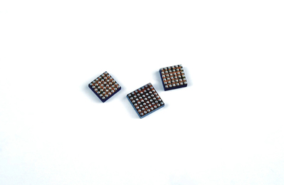
In the last days of the Mobile World Congress in Barcelona, Samsung Electronics announced a wide range of new products, including two Exynos processors, two CMOS image sensors, as well as a third-generation 45-nm NFC IC chip and an energy-efficient Wi-Fi module for use in modern smartphones and tablets.
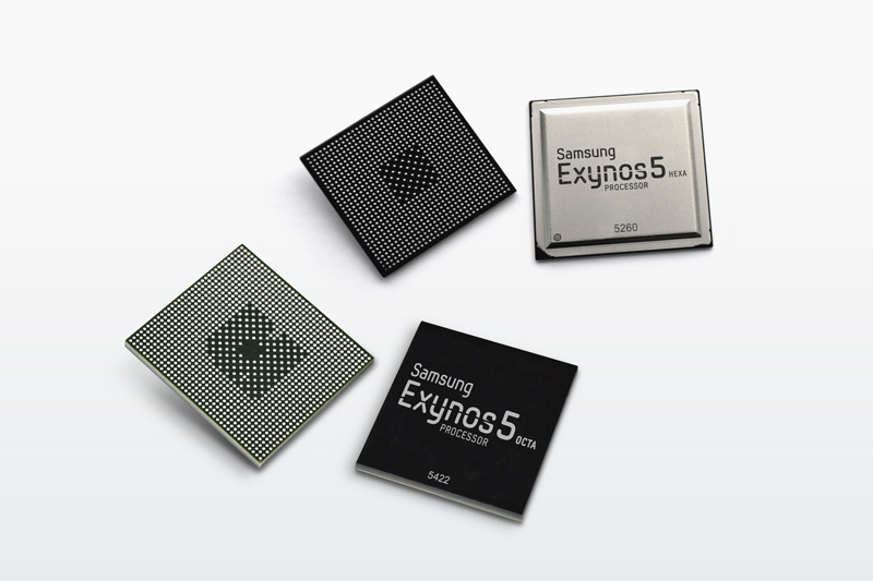
The new Samsung Exynos 5422 processor is based on the 28-nm process technology and is part of the Exynos 5 Octa family. It has eight cores — four high-performance, high-performance cores (ARM Cortex A15, up to 2.1 GHz), and four low-power cores for simple tasks (ARM Cortex A7, up to 1.5 GHz). In comparison with previous processors of the Exynos 5 Octa line, the new solution provides up to 34% higher performance. The Exynos 5422 single-chip system is built on the basis of an optimized ARM big.LITTLE architecture and supports HMP (Heterogeneous Multi-Processing) technology, which allows you to use all the processor cores simultaneously.
')
To support high-resolution displays requiring higher data rates and throughput, such as WQHD (2560 x 1440) and WQXGA (2560 x 1600), Samsung has implemented a new image compression solution (MIC) and adaptive hibernation technology. Thanks to the advanced MIC technology, the data displayed on the mobile device screen is halved and minimizes memory bandwidth requirements using only four MIPI (Mobile Industry Processor Interface) lines. To further reduce power consumption, the adaptive hibernation algorithm detects still fragments of dynamic images and freezes data transmission. Both technologies are implemented in conjunction with Samsung's IC mobile display driver (S6E3HA0 for WQHD and S6E3FA2 for FHD, respectively), and also reduce power consumption by 10% compared to previous generation technologies. Also, the new SoC will please the multi-format codec (MFC), which supports 4K UHD resolution.
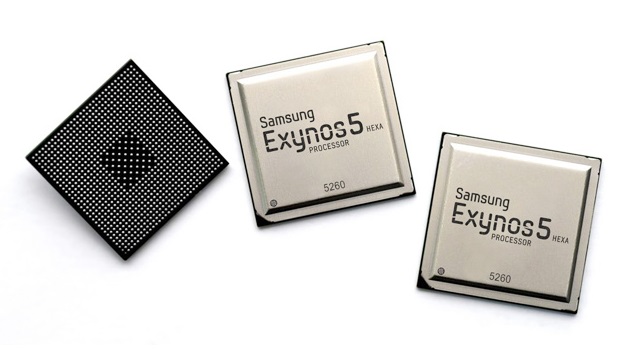
Another addition to the Exynos family is the Exynos 5 Hexa processor (Exynos 5260). This is a six-core chipset with two high-performance ARM Cortex A15 cores operating at 1.7 GHz and four low-power ARM Cortex A7 cores operating at 1.3 GHz. This processor also uses ARM big.LITTLE HMP technology to provide an increased level of performance compared to earlier processors of the Exynos 5 Dual series.
Exynos 5260 is equipped with a built-in eDP interface (embedded Display Port) and has a memory bandwidth of up to 12.8 GB / s, and also supports the screen resolution WQXGA (2560 x 1600). In addition, the video codec was integrated into the chipset, which allows playback of Full HD video (1080p) at speeds up to 60 frames per second with encoding / decoding of various standards, such as H.264, MPEG4 and VP8. Exynos 5 Hexa 5260 has already been launched into mass production, and the conveyors from Exynos 5 Octa 5422 will be launched before the end of the first quarter.
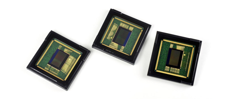
In addition to the Exynos processors, Samsung introduced new CMOS image sensors with a resolution of 13 megapixels and 16 megapixels with support for ISOCELL technology, which significantly increase sensitivity and effectively control the absorption of electrons, which leads to increased color accuracy even in low light conditions. The ISOCELL modules are significantly superior to BSI in terms of characteristics: the overall quality of photos is 30% better, the “noise” is reduced by 30%, and the viewing angle becomes 20% wider. The pixel size in the ISOCELL module is 1.12 µm.
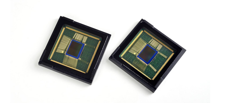
The older 16 megapixel model can shoot video at 60 frames per second and with Full HD resolution at an aspect ratio of 16: 9 (with a maximum resolution of only 30 frames per second). Mass production of cameras with this sensor on board will begin this month. The 13-megapixel version of the ISOCELL module will also receive WDR technology for “smart” video capture when shooting at 30 frames per second, thanks to a new software processing algorithm for improving image quality in low light conditions. Production of these CMOS sensors will begin in the second quarter of this year.
Another interesting novelty presented at the Mobile World Congress was the third generation NFC chip. This is the industry's first 45-nm NFC IC chip, which allows you to easily and safely update the firmware of a mobile device, as well as having low power consumption. The antenna of the new development is recognized as the smallest in size and has an improved radio frequency reception / transmission, which gives greater flexibility to designers of mobile devices. This was made possible thanks to Samsung's patented Smart Antenna technology, which optimizes the resistance of both the receiving and emitting parts of the antenna to increase the sensitivity and energy efficiency of the NFC chip. This device is scheduled for launch in mass production in the second quarter of 2014.
Samsung has also announced its first S5N2120 wireless solution, including for the growing Internet of Things market. Who does not know, the “Internet of things” from a programmatic point of view is the acquisition and collection of data with their subsequent transfer, followed by user interaction. The new energy-efficient Wi-Fi module supports IEEE 802.11 B / G / N Wi-Fi 2.4 GHz standards and is small in size, which is very important for a wide range of solutions. The module has a built-in microblock control (MCU) with a power amplifier, power management, audio codec and microphone functions. Using this microblock control, OEM customers can easily rebuild existing projects by incorporating Wi-Fi connectivity into them. This allows you to spend less time developing a mobile device and use engineering resources to a lesser extent. Such flexibility of the Wi-Fi module, along with high performance and a small placement area, is optimal for solutions that are limited by a small battery capacity, such as Wi-Fi speakers, headphones, remote controls, digital and sports cameras, smart heat meters and cooling, sensors and other types of IoT and M2M solutions. Samsung's new mobile Wi-Fi module S5N2120 is in the testing stage and will go into mass production in the second quarter of 2014.
In the last days of the Mobile World Congress in Barcelona, Samsung Electronics announced a wide range of new products, including two Exynos processors, two CMOS image sensors, as well as a third-generation 45-nm NFC IC chip and an energy-efficient Wi-Fi module for use in modern smartphones and tablets.
The new Samsung Exynos 5422 processor is based on the 28-nm process technology and is part of the Exynos 5 Octa family. It has eight cores — four high-performance, high-performance cores (ARM Cortex A15, up to 2.1 GHz), and four low-power cores for simple tasks (ARM Cortex A7, up to 1.5 GHz). In comparison with previous processors of the Exynos 5 Octa line, the new solution provides up to 34% higher performance. The Exynos 5422 single-chip system is built on the basis of an optimized ARM big.LITTLE architecture and supports HMP (Heterogeneous Multi-Processing) technology, which allows you to use all the processor cores simultaneously.
')
To support high-resolution displays requiring higher data rates and throughput, such as WQHD (2560 x 1440) and WQXGA (2560 x 1600), Samsung has implemented a new image compression solution (MIC) and adaptive hibernation technology. Thanks to the advanced MIC technology, the data displayed on the mobile device screen is halved and minimizes memory bandwidth requirements using only four MIPI (Mobile Industry Processor Interface) lines. To further reduce power consumption, the adaptive hibernation algorithm detects still fragments of dynamic images and freezes data transmission. Both technologies are implemented in conjunction with Samsung's IC mobile display driver (S6E3HA0 for WQHD and S6E3FA2 for FHD, respectively), and also reduce power consumption by 10% compared to previous generation technologies. Also, the new SoC will please the multi-format codec (MFC), which supports 4K UHD resolution.
Another addition to the Exynos family is the Exynos 5 Hexa processor (Exynos 5260). This is a six-core chipset with two high-performance ARM Cortex A15 cores operating at 1.7 GHz and four low-power ARM Cortex A7 cores operating at 1.3 GHz. This processor also uses ARM big.LITTLE HMP technology to provide an increased level of performance compared to earlier processors of the Exynos 5 Dual series.
Exynos 5260 is equipped with a built-in eDP interface (embedded Display Port) and has a memory bandwidth of up to 12.8 GB / s, and also supports the screen resolution WQXGA (2560 x 1600). In addition, the video codec was integrated into the chipset, which allows playback of Full HD video (1080p) at speeds up to 60 frames per second with encoding / decoding of various standards, such as H.264, MPEG4 and VP8. Exynos 5 Hexa 5260 has already been launched into mass production, and the conveyors from Exynos 5 Octa 5422 will be launched before the end of the first quarter.
In addition to the Exynos processors, Samsung introduced new CMOS image sensors with a resolution of 13 megapixels and 16 megapixels with support for ISOCELL technology, which significantly increase sensitivity and effectively control the absorption of electrons, which leads to increased color accuracy even in low light conditions. The ISOCELL modules are significantly superior to BSI in terms of characteristics: the overall quality of photos is 30% better, the “noise” is reduced by 30%, and the viewing angle becomes 20% wider. The pixel size in the ISOCELL module is 1.12 µm.
The older 16 megapixel model can shoot video at 60 frames per second and with Full HD resolution at an aspect ratio of 16: 9 (with a maximum resolution of only 30 frames per second). Mass production of cameras with this sensor on board will begin this month. The 13-megapixel version of the ISOCELL module will also receive WDR technology for “smart” video capture when shooting at 30 frames per second, thanks to a new software processing algorithm for improving image quality in low light conditions. Production of these CMOS sensors will begin in the second quarter of this year.
Another interesting novelty presented at the Mobile World Congress was the third generation NFC chip. This is the industry's first 45-nm NFC IC chip, which allows you to easily and safely update the firmware of a mobile device, as well as having low power consumption. The antenna of the new development is recognized as the smallest in size and has an improved radio frequency reception / transmission, which gives greater flexibility to designers of mobile devices. This was made possible thanks to Samsung's patented Smart Antenna technology, which optimizes the resistance of both the receiving and emitting parts of the antenna to increase the sensitivity and energy efficiency of the NFC chip. This device is scheduled for launch in mass production in the second quarter of 2014.
Samsung has also announced its first S5N2120 wireless solution, including for the growing Internet of Things market. Who does not know, the “Internet of things” from a programmatic point of view is the acquisition and collection of data with their subsequent transfer, followed by user interaction. The new energy-efficient Wi-Fi module supports IEEE 802.11 B / G / N Wi-Fi 2.4 GHz standards and is small in size, which is very important for a wide range of solutions. The module has a built-in microblock control (MCU) with a power amplifier, power management, audio codec and microphone functions. Using this microblock control, OEM customers can easily rebuild existing projects by incorporating Wi-Fi connectivity into them. This allows you to spend less time developing a mobile device and use engineering resources to a lesser extent. Such flexibility of the Wi-Fi module, along with high performance and a small placement area, is optimal for solutions that are limited by a small battery capacity, such as Wi-Fi speakers, headphones, remote controls, digital and sports cameras, smart heat meters and cooling, sensors and other types of IoT and M2M solutions. Samsung's new mobile Wi-Fi module S5N2120 is in the testing stage and will go into mass production in the second quarter of 2014.
Source: https://habr.com/ru/post/214897/
All Articles